SBAS674A July 2014 – September 2016 ADS1148-Q1
PRODUCTION DATA.
- 1 Features
- 2 Applications
- 3 Description
- 4 Revision History
- 5 Pin Configuration and Functions
- 6 Specifications
- 7 Parameter Measurement Information
-
8 Detailed Description
- 8.1 Overview
- 8.2 Functional Block Diagram
- 8.3
Feature Description
- 8.3.1 ADC Input and Multiplexer
- 8.3.2 Low-Noise PGA
- 8.3.3 Clock Source
- 8.3.4 Modulator
- 8.3.5 Digital Filter
- 8.3.6 Voltage Reference Input
- 8.3.7 Internal Voltage Reference
- 8.3.8 Excitation Current Sources
- 8.3.9 Sensor Detection
- 8.3.10 Bias Voltage Generation
- 8.3.11 General-Purpose Digital I/O
- 8.3.12 System Monitor
- 8.4 Device Functional Modes
- 8.5
Programming
- 8.5.1 Digital Interface
- 8.5.2 Data Format
- 8.5.3
Commands
- 8.5.3.1 WAKEUP (0000 000x)
- 8.5.3.2 SLEEP (0000 001x)
- 8.5.3.3 SYNC (0000 010x)
- 8.5.3.4 RESET (0000 011x)
- 8.5.3.5 RDATA (0001 001x)
- 8.5.3.6 RDATAC (0001 010x)
- 8.5.3.7 SDATAC (0001 011x)
- 8.5.3.8 RREG (0010 rrrr, 0000 nnnn)
- 8.5.3.9 WREG (0100 rrrr, 0000 nnnn)
- 8.5.3.10 SYSOCAL (0110 0000)
- 8.5.3.11 SYSGCAL (0110 0001)
- 8.5.3.12 SELFOCAL (0110 0010)
- 8.5.3.13 NOP (1111 1111)
- 8.5.3.14 Restricted Command (1111 0001)
- 8.6
Register Maps
- 8.6.1 Register Map
- 8.6.2
Detailed Register Definitions
- 8.6.2.1 MUX0—Multiplexer Control Register 0 (address = 00h) [reset = 01h]
- 8.6.2.2 VBIAS—Bias Voltage Register (address = 01h) [reset = 00h]
- 8.6.2.3 MUX1—Multiplexer Control Register 1 (address = 02h) [reset = x0h]
- 8.6.2.4 SYS0—System Control Register 0 (address = 03h) [reset = 00h]
- 8.6.2.5 OFC—Offset Calibration Coefficient Register (address = 04h, 05h, 06h) [reset = 00h, 00h, 00h]
- 8.6.2.6 FSC—Full-Scale Calibration Coefficient Register (address = 07h, 08h, 09h) [reset = 00h, 00h, 40h]
- 8.6.2.7 IDAC0—IDAC Control Register 0 (address = 0Ah) [reset = x0h]
- 8.6.2.8 IDAC1—IDAC Control Register 1 (address = 0Bh) [reset = FFh]
- 8.6.2.9 GPIOCFG—GPIO Configuration Register (address = 0Ch) [reset = 00h]
- 8.6.2.10 GPIODIR—GPIO Direction Register (address = 0Dh) [reset = 00h]
- 8.6.2.11 GPIODAT—GPIO Data Register (address = 0Eh) [reset = 00h]
-
9 Application and Implementation
- 9.1
Application Information
- 9.1.1 Serial Interface Connections
- 9.1.2 Analog Input Filtering
- 9.1.3 External Reference and Ratiometric Measurements
- 9.1.4 Establishing a Proper Common-Mode Input Voltage
- 9.1.5 Isolated (or Floating) Sensor Inputs
- 9.1.6 Unused Inputs and Outputs
- 9.1.7 Pseudo Code Example
- 9.1.8 Channel Multiplexing Example
- 9.1.9 Power-Down Mode Example
- 9.2 Typical Applications
- 9.3 Do's and Don'ts
- 9.1
Application Information
- 10Power Supply Recommendations
- 11Layout
- 12Device and Documentation Support
- 13Mechanical, Packaging, and Orderable Information
Package Options
Mechanical Data (Package|Pins)
- PW|28
Thermal pad, mechanical data (Package|Pins)
Orderable Information
1 Features
- Qualified for Automotive Applications
- AEC-Q100 Qualified with the Following Results:
- Temperature Grade 1: –40°C to +125°C
- HBM ESD Classification 2
- CDM ESD Classification C5
- Programmable Gain: 1 V/V to 128 V/V
- Programmable Data Rates: 5 SPS to 2 kSPS
- Single-Cycle Settling for All Data Rates
- Analog Multiplexer With 8 Independently Selectable Inputs
- Dual-Matched Programmable Excitation Current Sources: 50 µA to 1.5 mA
- Internal 2.048-V Voltage Reference
- Internal 4.096-MHz Oscillator
- Internal Temperature Sensor
- Open Sensor Detection
- Power-Supply and External Reference Monitoring
- Self and System Calibration
- 8 General-Purpose I/Os
- SPI-Compatible Serial Interface
- Analog Supply: Unipolar (2.7 V to 5.25 V) or
Bipolar (±2.5 V) - Digital Supply: 2.7 V to 5.25 V
2 Applications
- Thermocouple-, RTD- and Thermistor-
Based Temperature Measurement Systems - Exhaust Gas Sensing (Soot, NOx, NH3, O2)
- Battery Management Systems (BMS)
- Multichannel Voltage and Current Monitoring
3 Description
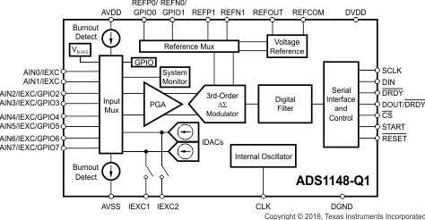
The ADS1148-Q1 is a highly-integrated, precision, 16-bit analog-to-digital converter (ADC) that includes many integrated features to reduce system cost and component count for sensor measurement applications. The device features a low-noise, programmable gain amplifier (PGA), a precision delta-sigma (ΔΣ) ADC with a single-cycle settling digital filter, and an internal oscillator. The
ADS1148-Q1 integrates a low-drift voltage reference, and two matched programmable excitation current sources (IDACs).
The device offers a fully flexible multiplexer that allows both positive and negative inputs to be selected independently. In addition, the multiplexer integrates sensor burn-out detection, voltage bias for thermocouples, system monitoring, and eight general-purpose digital I/Os (GPIOs). The PGA provides selectable gains up to 128 V/V. These features provide a complete front-end solution for temperature sensor measurement applications, including thermocouples, thermistors, and resistance temperature detectors (RTDs), and other small-signal measurements. The digital filter settles in a single cycle to support fast channel cycling when using the input multiplexer and provides data rates up to 2 kSPS. For data rates of 20 SPS or less, both the 50-Hz and 60-Hz interference are rejected by the filter.
Device Information(1)
| PART NUMBER | PACKAGE | BODY SIZE (NOM) |
|---|---|---|
| ADS1148-Q1 | TSSOP (28) | 9.70 mm × 4.40 mm |
- For all available packages, see the orderable addendum at the end of the datasheet.
Functional Block Diagram
