SBAS924A July   2018  – November 2018 ADS1219

PRODUCTION DATA.  

  1. Features
  2. Applications
  3. Description
    1.     Device Images
      1.      Voltage, Current, and Temperature Monitoring Application
  4. Revision History
  5. Pin Configuration and Functions
    1.     Pin Functions
  6. Specifications
    1. 6.1 Absolute Maximum Ratings
    2. 6.2 ESD Ratings
    3. 6.3 Recommended Operating Conditions
    4. 6.4 Thermal Information
    5. 6.5 Electrical Characteristics
    6. 6.6 I2C Timing Requirements
    7. 6.7 I2C Switching Characteristics
    8. 6.8 Typical Characteristics
  7. Parameter Measurement Information
    1. 7.1 Noise Performance
  8. Detailed Description
    1. 8.1 Overview
    2. 8.2 Functional Block Diagram
    3. 8.3 Feature Description
      1. 8.3.1 Multiplexer
      2. 8.3.2 Rail-to-Rail Input Buffers and Programmable Gain Stage
      3. 8.3.3 Voltage Reference
      4. 8.3.4 Modulator and Internal Oscillator
      5. 8.3.5 Digital Filter
      6. 8.3.6 Conversion Times
      7. 8.3.7 Offset Calibration
    4. 8.4 Device Functional Modes
      1. 8.4.1 Power-Up and Reset
        1. 8.4.1.1 Power-On Reset
        2. 8.4.1.2 RESET Pin
        3. 8.4.1.3 Reset by Command
      2. 8.4.2 Conversion Modes
        1. 8.4.2.1 Single-Shot Conversion Mode
        2. 8.4.2.2 Continuous Conversion Mode
      3. 8.4.3 Power-Down Mode
    5. 8.5 Programming
      1. 8.5.1 I2C Interface
        1. 8.5.1.1 I2C Address
        2. 8.5.1.2 Serial Clock (SCL) and Serial Data (SDA)
        3. 8.5.1.3 Data Ready (DRDY)
        4. 8.5.1.4 Interface Speed
        5. 8.5.1.5 Data Transfer Protocol
        6. 8.5.1.6 I2C General Call (Software Reset)
        7. 8.5.1.7 Timeout
      2. 8.5.2 Data Format
      3. 8.5.3 Commands
        1. 8.5.3.1 Command Latching
        2. 8.5.3.2 RESET (0000 011x)
        3. 8.5.3.3 START/SYNC (0000 100x)
        4. 8.5.3.4 POWERDOWN (0000 001x)
        5. 8.5.3.5 RDATA (0001 xxxx)
        6. 8.5.3.6 RREG (0010 0rxx)
        7. 8.5.3.7 WREG (0100 00xx dddd dddd)
      4. 8.5.4 Reading Data and Monitoring for New Conversion Results
    6. 8.6 Register Map
      1. 8.6.1 Configuration and Status Registers
      2. 8.6.2 Register Descriptions
        1. 8.6.2.1 Configuration Register (address = 0h) [reset = 00h]
          1. Table 10. Configuration Register Field Descriptions
        2. 8.6.2.2 Status Register (address = 1h) [reset = 00h]
          1. Table 11. Status Register Field Descriptions
  9. Application and Implementation
    1. 9.1 Application Information
      1. 9.1.1 Interface Connections
      2. 9.1.2 Connecting Multiple Devices on the Same I2C Bus
      3. 9.1.3 Unused Inputs and Outputs
      4. 9.1.4 Analog Input Filtering
      5. 9.1.5 External Reference and Ratiometric Measurements
      6. 9.1.6 Establishing Proper Limits on the Absolute Input Voltage
      7. 9.1.7 Pseudo Code Example
    2. 9.2 Typical Application
      1. 9.2.1 Design Requirements
      2. 9.2.2 Detailed Design Procedure
        1. 9.2.2.1 Voltage Monitoring
        2. 9.2.2.2 High-Side Current Measurement
        3. 9.2.2.3 Thermistor Measurement
        4. 9.2.2.4 Register Settings
      3. 9.2.3 Application Curve
  10. 10Power Supply Recommendations
    1. 10.1 Power-Supply Sequencing
    2. 10.2 Power-Supply Decoupling
  11. 11Layout
    1. 11.1 Layout Guidelines
    2. 11.2 Layout Example
  12. 12Device and Documentation Support
    1. 12.1 Device Support
      1. 12.1.1 Third-Party Products Disclaimer
    2. 12.2 Documentation Support
      1. 12.2.1 Related Documentation
    3. 12.3 Receiving Notification of Documentation Updates
    4. 12.4 Community Resources
    5. 12.5 Trademarks
    6. 12.6 Electrostatic Discharge Caution
    7. 12.7 Glossary
  13. 13Mechanical, Packaging, and Orderable Information

Package Options

Mechanical Data (Package|Pins)
Thermal pad, mechanical data (Package|Pins)
Orderable Information

Multiplexer

Figure 27 shows the flexible input multiplexer of the device. Either four single-ended signals, two differential signals, or a combination of two single-ended signals and one differential signal can be measured. The positive (AINP) and negative (AINN) inputs selected for measurement are configured by three bits (MUX[2:0]) in the configuration register. When single-ended signals need to be measured, the negative ADC input (AINN) can internally be connected to AGND by a switch within the multiplexer.
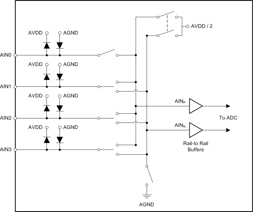
ADS1219 mux_bas924.gifFigure 27. Analog Input Multiplexer

Electrostatic discharge (ESD) diodes to AVDD and AGND protect the inputs. The absolute voltage on any input must stay within the range provided by Equation 3 to prevent the ESD diodes from turning on:

Equation 3. AGND – 0.3 V < V(AINx) < AVDD + 0.3 V

If the voltages on the input pins have any potential to violate these conditions, external Schottky clamp diodes or series resistors may be required to limit the input current to safe values (see the Absolute Maximum Ratings table). Overdriving an unused input on the device can affect conversions taking place on other input pins.