SBAS751B October   2017  – October 2018 ADS122C04

PRODUCTION DATA.  

  1. Features
  2. Applications
  3. Description
    1.     Device Images
      1.      K-Type Thermocouple Measurement
  4. Revision History
  5. Pin Configuration and Functions
    1.     Pin Functions
  6. Specifications
    1. 6.1 Absolute Maximum Ratings
    2. 6.2 ESD Ratings
    3. 6.3 Recommended Operating Conditions
    4. 6.4 Thermal Information
    5. 6.5 Electrical Characteristics
    6. 6.6 I2C Timing Requirements
    7. 6.7 I2C Switching Characteristics
    8. 6.8 Typical Characteristics
  7. Parameter Measurement Information
    1. 7.1 Noise Performance
  8. Detailed Description
    1. 8.1 Overview
    2. 8.2 Functional Block Diagram
    3. 8.3 Feature Description
      1. 8.3.1  Multiplexer
      2. 8.3.2  Low-Noise Programmable Gain Stage
        1. 8.3.2.1 PGA Input Voltage Requirements
        2. 8.3.2.2 Bypassing the PGA
      3. 8.3.3  Voltage Reference
      4. 8.3.4  Modulator and Internal Oscillator
      5. 8.3.5  Digital Filter
      6. 8.3.6  Conversion Times
      7. 8.3.7  Excitation Current Sources
      8. 8.3.8  Sensor Detection
      9. 8.3.9  System Monitor
      10. 8.3.10 Temperature Sensor
        1. 8.3.10.1 Converting From Temperature to Digital Codes
          1. 8.3.10.1.1 For Positive Temperatures (For Example, 50°C):
          2. 8.3.10.1.2 For Negative Temperatures (For Example, –25°C):
        2. 8.3.10.2 Converting From Digital Codes to Temperature
      11. 8.3.11 Offset Calibration
      12. 8.3.12 Conversion Data Counter
      13. 8.3.13 Data Integrity Features
    4. 8.4 Device Functional Modes
      1. 8.4.1 Power-Up and Reset
        1. 8.4.1.1 Power-On Reset
        2. 8.4.1.2 RESET Pin
        3. 8.4.1.3 Reset by Command
      2. 8.4.2 Conversion Modes
        1. 8.4.2.1 Single-Shot Conversion Mode
        2. 8.4.2.2 Continuous Conversion Mode
      3. 8.4.3 Operating Modes
        1. 8.4.3.1 Normal Mode
        2. 8.4.3.2 Turbo Mode
        3. 8.4.3.3 Power-Down Mode
    5. 8.5 Programming
      1. 8.5.1 I2C Interface
        1. 8.5.1.1 I2C Address
        2. 8.5.1.2 Serial Clock (SCL) and Serial Data (SDA)
        3. 8.5.1.3 Data Ready (DRDY)
        4. 8.5.1.4 Interface Speed
        5. 8.5.1.5 Data Transfer Protocol
        6. 8.5.1.6 I2C General Call (Software Reset)
        7. 8.5.1.7 Timeout
      2. 8.5.2 Data Format
      3. 8.5.3 Commands
        1. 8.5.3.1 Command Latching
        2. 8.5.3.2 RESET (0000 011x)
        3. 8.5.3.3 START/SYNC (0000 100x)
        4. 8.5.3.4 POWERDOWN (0000 001x)
        5. 8.5.3.5 RDATA (0001 xxxx)
        6. 8.5.3.6 RREG (0010 rrxx)
        7. 8.5.3.7 WREG (0100 rrxx dddd dddd)
      4. 8.5.4 Reading Data and Monitoring for New Conversion Results
      5. 8.5.5 Data Integrity
    6. 8.6 Register Map
      1. 8.6.1 Configuration Registers
      2. 8.6.2 Register Descriptions
        1. 8.6.2.1 Configuration Register 0 (address = 00h) [reset = 00h]
          1. Table 19. Configuration Register 0 Field Descriptions
        2. 8.6.2.2 Configuration Register 1 (address = 01h) [reset = 00h]
          1. Table 20. Configuration Register 1 Field Descriptions
        3. 8.6.2.3 Configuration Register 2 (address = 02h) [reset = 00h]
          1. Table 22. Configuration Register 2 Field Descriptions
        4. 8.6.2.4 Configuration Register 3 (address = 03h) [reset = 00h]
          1. Table 23. Configuration Register 3 Field Descriptions
  9. Application and Implementation
    1. 9.1 Application Information
      1. 9.1.1 Interface Connections
      2. 9.1.2 Connecting Multiple Devices on the Same I2C Bus
      3. 9.1.3 Unused Inputs and Outputs
      4. 9.1.4 Analog Input Filtering
      5. 9.1.5 External Reference and Ratiometric Measurements
      6. 9.1.6 Establishing Proper Limits on the Absolute Input Voltage
      7. 9.1.7 Pseudo Code Example
    2. 9.2 Typical Applications
      1. 9.2.1 K-Type Thermocouple Measurement (–200°C to +1250°C)
        1. 9.2.1.1 Design Requirements
        2. 9.2.1.2 Detailed Design Procedure
        3. 9.2.1.3 Application Curves
      2. 9.2.2 3-Wire RTD Measurement (–200°C to +850°C)
        1. 9.2.2.1 Design Requirements
        2. 9.2.2.2 Detailed Design Procedure
          1. 9.2.2.2.1 Design Variations for 2-Wire and 4-Wire RTD Measurements
        3. 9.2.2.3 Application Curves
      3. 9.2.3 Resistive Bridge Measurement
        1. 9.2.3.1 Design Requirements
        2. 9.2.3.2 Detailed Design Procedure
  10. 10Power Supply Recommendations
    1. 10.1 Power-Supply Sequencing
    2. 10.2 Power-Supply Decoupling
  11. 11Layout
    1. 11.1 Layout Guidelines
    2. 11.2 Layout Example
  12. 12Device and Documentation Support
    1. 12.1 Device Support
      1. 12.1.1 Third-Party Products Disclaimer
    2. 12.2 Documentation Support
      1. 12.2.1 Related Documentation
    3. 12.3 Receiving Notification of Documentation Updates
    4. 12.4 Community Resources
    5. 12.5 Trademarks
    6. 12.6 Electrostatic Discharge Caution
    7. 12.7 Glossary
  13. 13Mechanical, Packaging, and Orderable Information

Package Options

Mechanical Data (Package|Pins)
Thermal pad, mechanical data (Package|Pins)
Orderable Information

Power-Supply Decoupling

Good power-supply decoupling is important to achieve optimum performance. As shown in Figure 80 and Figure 81, AVDD, AVSS (when using a bipolar supply), and DVDD must be decoupled with at least a 0.1-µF capacitor. Place the bypass capacitors as close to the power-supply pins of the device as possible using low-impedance connections. TI recommends using multi-layer ceramic chip capacitors (MLCCs) that offer low equivalent series resistance (ESR) and inductance (ESL) characteristics for power-supply decoupling purposes. For very sensitive systems, or for systems in harsh noise environments, avoiding the use of vias for connecting the capacitors to the device pins may offer superior noise immunity. The use of multiple vias in parallel lowers the overall inductance and is beneficial for connections to ground planes. Connect analog and digital grounds together as close to the device as possible.
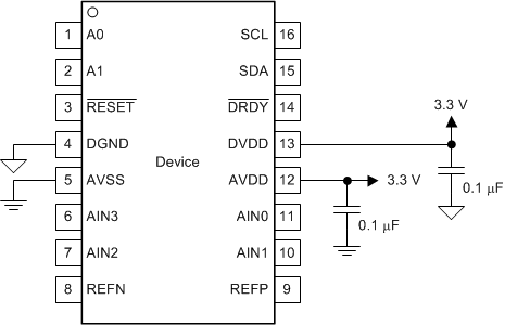
ADS122C04 ai_unipolar_supply_bas751.gifFigure 80. Unipolar Analog Power Supply
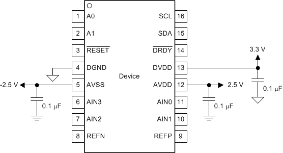
ADS122C04 ai_bipolar_supply_bas751.gifFigure 81. Bipolar Analog Power Supply