SBAS502C December   2011  – April 2020 ADS1291 , ADS1292 , ADS1292R

PRODUCTION DATA.  

  1. Features
  2. Applications
    1.     Simplified Block Diagram
  3. Description
  4. Revision History
  5. Pin Configuration and Functions
    1.     Pin Functions
  6. Specifications
    1. 6.1 Absolute Maximum Ratings
    2. 6.2 ESD Ratings
    3. 6.3 Recommended Operating Conditions
    4. 6.4 Thermal Information
    5. 6.5 Electrical Characteristics
    6. 6.6 Timing Requirements
    7. 6.7 Typical Characteristics
  7. Parameter Measurement Information
    1. 7.1 Noise Measurements
  8. Detailed Description
    1. 8.1 Overview
    2. 8.2 Functional Block Diagram
    3. 8.3 Feature Description
      1. 8.3.1  EMI Filter
      2. 8.3.2  Input Multiplexer
        1. 8.3.2.1 Device Noise Measurements
        2. 8.3.2.2 Test Signals (TestP and TestN)
        3. 8.3.2.3 Auxiliary Differential Input (RESP_MODN/IN3N, RESP_MODN/IN3P)
        4. 8.3.2.4 Temperature Sensor (TEMPP, TEMPN)
        5. 8.3.2.5 Supply Measurements (MVDDP, MVDDN)
        6. 8.3.2.6 Lead-Off Excitation Signals (LoffP, LoffN)
        7. 8.3.2.7 Auxiliary Single-Ended Input
      3. 8.3.3  Analog Input
      4. 8.3.4  PGA Settings and Input Range
        1. 8.3.4.1 Input Common-Mode Range
        2. 8.3.4.2 Input Differential Dynamic Range
        3. 8.3.4.3 ADC ΔΣ Modulator
      5. 8.3.5  Digital Decimation Filter
        1. 8.3.5.1 Sinc Filter Stage (sinx / x)
      6. 8.3.6  Reference
      7. 8.3.7  Clock
      8. 8.3.8  Data Format
      9. 8.3.9  Multiple Device Configuration
        1. 8.3.9.1 Standard Mode
      10. 8.3.10 ECG-Specific Functions
        1. 8.3.10.1 Input Multiplexer (Rerouting the Right Leg Drive Signal)
          1. 8.3.10.1.1 Input Multiplexer (Measuring the Right Leg Drive Signal)
        2. 8.3.10.2 Lead-Off Detection
          1. 8.3.10.2.1 DC Lead-Off
          2. 8.3.10.2.2 AC Lead-Off
          3. 8.3.10.2.3 RLD Lead-Off
          4. 8.3.10.2.4 Right Leg Drive (RLD DC Bias Circuit)
            1. 8.3.10.2.4.1 RLD Configuration With Multiple Devices
        3. 8.3.10.3 PACE Detect
        4. 8.3.10.4 Respiration
          1. 8.3.10.4.1 Internal Respiration Circuitry With Internal Clock (ADS1292R)
          2. 8.3.10.4.2 Internal Respiration Circuitry With External Clock (ADS1292R)
      11. 8.3.11 Setting the Device for Basic Data Capture
        1. 8.3.11.1 Lead-Off
    4. 8.4 Device Functional Modes
    5. 8.5 Programming
      1. 8.5.1 SPI Interface
        1. 8.5.1.1  Chip Select (CS)
        2. 8.5.1.2  Serial Clock (SCLK)
        3. 8.5.1.3  Data Input (DIN)
        4. 8.5.1.4  Data Output (DOUT)
        5. 8.5.1.5  Data Retrieval
        6. 8.5.1.6  Data Ready (DRDY)
        7. 8.5.1.7  GPIO
        8. 8.5.1.8  Power-Down and Reset (PWDN/RESET)
        9. 8.5.1.9  START
        10. 8.5.1.10 Settling Time
        11. 8.5.1.11 Continuous Mode
        12. 8.5.1.12 Single-Shot Mode
      2. 8.5.2 SPI Command Definitions
        1. 8.5.2.1  WAKEUP: Exit STANDBY Mode
        2. 8.5.2.2  STANDBY: Enter STANDBY Mode
        3. 8.5.2.3  RESET: Reset Registers to Default Values
        4. 8.5.2.4  START: Start Conversions
        5. 8.5.2.5  STOP: Stop Conversions
        6. 8.5.2.6  OFFSETCAL: Channel Offset Calibration
        7. 8.5.2.7  RDATAC: Read Data Continuous
        8. 8.5.2.8  SDATAC: Stop Read Data Continuous
        9. 8.5.2.9  RDATA: Read Data
        10. 8.5.2.10 Sending Multi-Byte Commands
        11. 8.5.2.11 RREG: Read From Register
        12. 8.5.2.12 WREG: Write to Register
    6. 8.6 Register Maps
      1. 8.6.1 User Register Description
        1. 8.6.1.1  ID: ID Control Register (Factory-Programmed, Read-Only) (address = 00h)
          1. Table 17. ID: ID Control Register (Factory-Programmed, Read-Only) Field Descriptions
        2. 8.6.1.2  CONFIG1: Configuration Register 1 (address = 01h)
          1. Table 18. CONFIG1: Configuration Register 1 Field Descriptions
        3. 8.6.1.3  CONFIG2: Configuration Register 2 (address = 02h)
          1. Table 19. CONFIG2: Configuration Register 2 Field Descriptions
        4. 8.6.1.4  LOFF: Lead-Off Control Register (address = 03h)
          1. Table 20. LOFF: Lead-Off Control Register Field Descriptions
        5. 8.6.1.5  CH1SET: Channel 1 Settings (address = 04h)
          1. Table 21. CH1SET: Channel 1 Settings Field Descriptions
        6. 8.6.1.6  CH2SET: Channel 2 Settings (address = 05h)
          1. Table 22. CH2SET: Channel 2 Settings Field Descriptions
        7. 8.6.1.7  RLD_SENS: Right Leg Drive Sense Selection (address = 06h)
          1. Table 23. RLD_SENS: Right Leg Drive Sense Selection Field Descriptions
        8. 8.6.1.8  LOFF_SENS: Lead-Off Sense Selection (address = 07h)
          1. Table 24. LOFF_SENS: Lead-Off Sense Selection Field Descriptions
        9. 8.6.1.9  LOFF_STAT: Lead-Off Status (address = 08h)
          1. Table 25. LOFF_STAT: Lead-Off Status Field Descriptions
        10. 8.6.1.10 RESP1: Respiration Control Register 1 (address = 09h)
          1. Table 26. RESP1: Respiration Control Register 1 Field Descriptions
        11. 8.6.1.11 RESP2: Respiration Control Register 2 (address = 0Ah)
          1. Table 27. RESP2: Respiration Control Register 2 Field Descriptions
        12. 8.6.1.12 GPIO: General-Purpose I/O Register (address = 0Bh)
          1. Table 28. GPIO: General-Purpose I/O Register Field Descriptions
  9. Application and Implementation
    1. 9.1 Application Information
    2. 9.2 Typical Application
      1. 9.2.1 Design Requirements
      2. 9.2.2 Detailed Design Procedure
      3. 9.2.3 Application Curves
  10. 10Power Supply Recommendations
    1. 10.1 Power-Up Sequencing
  11. 11Layout
    1. 11.1 Layout Guidelines
      1. 11.1.1 PCB Layout
        1. 11.1.1.1 Power Supplies and Grounding
          1. 11.1.1.1.1 Connecting the Device to Unipolar (+3 V or +1.8 V) Supplies
          2. 11.1.1.1.2 Connecting the Device to Bipolar (±1.5 V or 1.8 V) Supplies
        2. 11.1.1.2 Shielding Analog Signal Paths
    2. 11.2 Layout Example
  12. 12Device and Documentation Support
    1. 12.1 Related Links
    2. 12.2 Receiving Notification of Documentation Updates
    3. 12.3 Support Resources
    4. 12.4 Trademarks
    5. 12.5 Electrostatic Discharge Caution
    6. 12.6 Glossary
  13. 13Mechanical, Packaging, and Orderable Information

Package Options

Mechanical Data (Package|Pins)
Thermal pad, mechanical data (Package|Pins)
Orderable Information

ADC ΔΣ Modulator

Each channel of the ADS1291, ADS1292, and ADS1292R has a 24-bit ΔΣ ADC. This converter uses a second-order modulator optimized for low-power applications. The modulator samples the input signal at the rate of fMOD = fCLK / 4 or fCLK / 16, as determined by the CLK_DIV bit. In both cases, the sampling clock has a typical value of 128 kHz. As in the case of any ΔΣ modulator, the ADS1291, ADS1292, and ADS1292R noise is shaped until fMOD / 2, as shown in Figure 24. The on-chip digital decimation filters explained in the Digital Decimation Filter section can be used to filter out the noise at higher frequencies. These on-chip decimation filters also provide antialias filtering. This feature of the ΔΣ converters drastically reduces the complexity of analog antialiasing filters that are typically needed with nyquist ADCs.
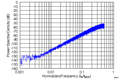
ADS1291 ADS1292 ADS1292R G001_BAS502.pngFigure 24. Power Spectral Density (PSD) of a ΔΣ Modulator (4-Bit Quantizer)