SBAS459K January 2010 – August 2015 ADS1294 , ADS1294R , ADS1296 , ADS1296R , ADS1298 , ADS1298R
PRODUCTION DATA.
- 1 Features
- 2 Applications
- 3 Description
- 4 Revision History
- 5 Device Comparison
- 6 Pin Configuration and Functions
- 7 Specifications
- 8 Parameter Measurement Information
-
9 Detailed Description
- 9.1 Overview
- 9.2 Functional Block Diagram
- 9.3
Feature Description
- 9.3.1
Analog Functionality
- 9.3.1.1 EMI Filter
- 9.3.1.2 Analog Input Structure
- 9.3.1.3
Input Multiplexer
- 9.3.1.3.1 Device Noise Measurements
- 9.3.1.3.2 Test Signals (TestP and TestN)
- 9.3.1.3.3 Auxiliary Differential Input (TESTP_PACE_OUT1, TESTN_PACE_OUT2)
- 9.3.1.3.4 Temperature Sensor (TempP, TempN)
- 9.3.1.3.5 Supply Measurements (MVDDP, MVDDN)
- 9.3.1.3.6 Lead-Off Excitation Signals (LoffP, LoffN)
- 9.3.1.3.7 Auxiliary Single-Ended Input
- 9.3.1.4 Analog Input
- 9.3.1.5 PGA Settings and Input Range
- 9.3.1.6 Reference
- 9.3.1.7
ECG-Specific Functions
- 9.3.1.7.1 Input Multiplexer (Rerouting The Right Leg Drive Signal)
- 9.3.1.7.2 Input Multiplexer (Measuring The Right Leg Drive Signal)
- 9.3.1.7.3 Wilson Central Terminal (WCT) and Chest Leads
- 9.3.1.7.4 Lead-Off Detection
- 9.3.1.7.5 RLD Lead-Off
- 9.3.1.7.6 Right Leg Drive (RLD) DC Bias Circuit
- 9.3.1.7.7 Pace Detect
- 9.3.1.7.8 Respiration
- 9.3.2 Digital Functionality
- 9.3.1
Analog Functionality
- 9.4 Device Functional Modes
- 9.5
Programming
- 9.5.1 SPI Interface
- 9.5.2
SPI Command Definitions
- 9.5.2.1 WAKEUP: Exit Standby Mode
- 9.5.2.2 STANDBY: Enter Standby Mode
- 9.5.2.3 RESET: Reset Registers to Default Values
- 9.5.2.4 START: Start Conversions
- 9.5.2.5 STOP: Stop Conversions
- 9.5.2.6 RDATAC: Read Data Continuous
- 9.5.2.7 SDATAC: Stop Read Data Continuous
- 9.5.2.8 RDATA: Read Data
- 9.5.2.9 Sending Multibyte Commands
- 9.5.2.10 RREG: Read From Register
- 9.5.2.11 WREG: Write to Register
- 9.6
Register Maps
- 9.6.1
Register Descriptions
- 9.6.1.1 ID: ID Control Register (address = 00h) (reset = xxh)
- 9.6.1.2 CONFIG1: Configuration Register 1 (address = 01h) (reset = 06h)
- 9.6.1.3 CONFIG2: Configuration Register 2 (address = 02h) (reset = 40h)
- 9.6.1.4 CONFIG3: Configuration Register 3 (address = 03h) (reset = 40h)
- 9.6.1.5 LOFF: Lead-Off Control Register (address = 04h) (reset = 00h)
- 9.6.1.6 CHnSET: Individual Channel Settings (n = 1 to 8) (address = 05h to 0Ch) (reset = 00h)
- 9.6.1.7 RLD_SENSP: RLD Positive Signal Derivation Register (address = 0Dh) (reset = 00h)
- 9.6.1.8 RLD_SENSN: RLD Negative Signal Derivation Register (address = 0Eh) (reset = 00h)
- 9.6.1.9 LOFF_SENSP: Positive Signal Lead-Off Detection Register (address = 0Fh) (reset = 00h)
- 9.6.1.10 LOFF_SENSN: Negative Signal Lead-Off Detection Register (address = 10h) (reset = 00h)
- 9.6.1.11 LOFF_FLIP: Lead-Off Flip Register (address = 11h) (reset = 00h)
- 9.6.1.12 LOFF_STATP: Lead-Off Positive Signal Status Register (address = 12h) (reset = 00h)
- 9.6.1.13 LOFF_STATN: Lead-Off Negative Signal Status Register (address = 13h) (reset = 00h)
- 9.6.1.14 GPIO: General-Purpose I/O Register (address = 14h) (reset = 0Fh)
- 9.6.1.15 PACE: Pace Detect Register (address = 15h) (reset = 00h)
- 9.6.1.16 RESP: Respiration Control Register (address = 16h) (reset = 00h)
- 9.6.1.17 CONFIG4: Configuration Register 4 (address = 17h) (reset = 00h)
- 9.6.1.18 WCT1: Wilson Central Terminal and Augmented Lead Control Register (address = 18h) (reset = 00h)
- 9.6.1.19 WCT2: Wilson Central Terminal Control Register (address = 18h) (reset = 00h)
- 9.6.1
Register Descriptions
- 10Application and Implementation
- 11Power Supply Recommendations
- 12Layout
- 13Device and Documentation Support
- 14Mechanical, Packaging, and Orderable Information
Package Options
Mechanical Data (Package|Pins)
- ZXG|64
Thermal pad, mechanical data (Package|Pins)
Orderable Information
11 Power Supply Recommendations
The ADS129x have three power supplies: AVDD, AVDD1, and DVDD. For best performance, both AVDD and AVDD1 must be as quiet as possible. AVDD1 provides the supply to the charge pump block and has transients at fCLK. Therefore, star connect AVDD1 and AVSS1 to AVDD and AVSS. It is important to eliminate noise from AVDD and AVDD1 that is nonsynchronous with ADS129x operation. Bypass each ADS129x supply with 1-μF and 0.1-μF solid ceramic capacitors. For best performance, place the digital circuits (DSP, microcontrollers, FPGAs, and so forth) in the system so that the return currents on those devices do not cross the analog return path of the ADS129x. Power the ADS129x from unipolar or bipolar supplies.
Use surface-mount, low-cost, low-profile, multilayer ceramic-type capacitors for decoupling. In most cases, the VCAP1 capacitor is also a multilayer ceramic; however, in systems where the board is subjected to high- or low-frequency vibration, install a nonferroelectric capacitor, such as a tantalum or class 1 capacitor (C0G or NPO). EIA class 2 and class 3 dielectrics such as (X7R, X5R, X8R, and so forth) are ferroelectric. The piezoelectric property of these capacitors can appear as electrical noise coming from the capacitor. When using internal reference, noise on the VCAP1 node results in performance degradation.
11.1 Power-Up Sequencing
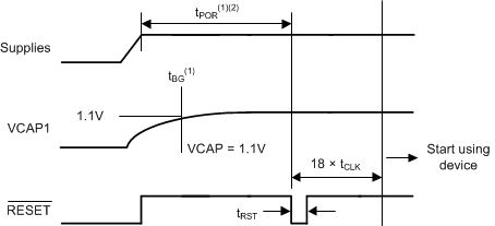
Before device power up, all digital and analog inputs must be low. At the time of power up, keep all of these signals low until the power supplies have stabilized, as shown in Figure 105.
Allow time for the supply voltages to reach their final value, and then begin supplying the master clock signal to the CLK pin. Wait for time tPOR, then transmit a reset pulse using either the RESET pin or RESET command to initialize the digital portion of the chip. Issue the reset after tPOR or after the VCAP1 voltage is greater than 1.1 V, whichever time is longer. Note that:
- tPOR is described in Table 38.
- The VCAP1 pin charge time is set by the RC time constant; see Figure 31.
After releasing the RESET pin, program the configuration registers; see the CONFIG1: Configuration Register 1 (address = 01h) (reset = 06h) section for details. The power-up sequence timing is shown in Table 38.

Table 38. Timing Requirements for Figure 105
| MIN | MAX | UNIT | ||
|---|---|---|---|---|
| tPOR | Wait after power up until reset | 218 | tCLK | |
| tRST | Reset low duration | 2 | tCLK | |
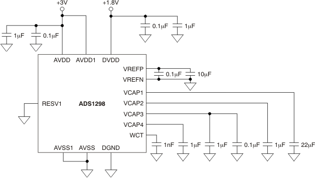
11.2 Connecting to Unipolar (3 V or 1.8 V) Supplies
Figure 106 illustrates the ADS129x connected to a unipolar supply. In this example, analog supply (AVDD) is referenced to analog ground (AVSS) and digital supplies (DVDD) are referenced to digital ground (DGND).

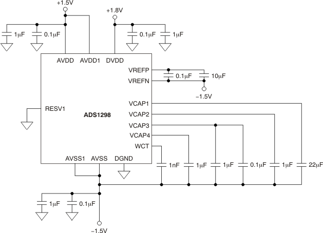
11.3 Connecting to Bipolar (±1.5 V or ±1.8 V) Supplies
Figure 107 illustrates the ADS129x connected to a bipolar supply. In this example, the analog supplies connect to the device analog supply (AVDD). This supply is referenced to the device analog return (AVSS), and the digital supply (DVDD) is referenced to the device digital ground return (DGND).
