SBAS950B October   2019  – February 2021 ADS131M08

PRODUCTION DATA  

  1. Features
  2. Applications
  3. Description
  4. Revision History
  5. Pin Configuration and Functions
  6. Specifications
    1. 6.1 Absolute Maximum Ratings
    2. 6.2 ESD Ratings
    3. 6.3 Recommended Operating Conditions
    4. 6.4 Thermal Information
    5. 6.5 Electrical Characteristics
    6. 6.6 Timing Requirements
    7. 6.7 Switching Characteristics
    8. 6.8 Timing Diagrams
    9. 6.9 Typical Characteristics
  7. Parameter Measurement Information
    1. 7.1 Noise Measurements
  8. Detailed Description
    1. 8.1 Overview
    2. 8.2 Functional Block Diagram
    3. 8.3 Feature Description
      1. 8.3.1  Input ESD Protection Circuitry
      2. 8.3.2  Input Multiplexer
      3. 8.3.3  Programmable Gain Amplifier (PGA)
      4. 8.3.4  Voltage Reference
      5. 8.3.5  Clocking and Power Modes
      6. 8.3.6  ΔΣ Modulator
      7. 8.3.7  Digital Filter
        1. 8.3.7.1 Digital Filter Implementation
          1. 8.3.7.1.1 Fast-Settling Filter
          2. 8.3.7.1.2 SINC3 and SINC3 + SINC1 Filter
        2. 8.3.7.2 Digital Filter Characteristic
      8. 8.3.8  DC Block Filter
      9. 8.3.9  Internal Test Signals
      10. 8.3.10 Channel Phase Calibration
      11. 8.3.11 Calibration Registers
      12. 8.3.12 Communication Cyclic Redundancy Check (CRC)
      13. 8.3.13 Register Map CRC
    4. 8.4 Device Functional Modes
      1. 8.4.1 Power-Up and Reset
        1. 8.4.1.1 Power-On Reset
        2. 8.4.1.2 SYNC/RESET Pin
        3. 8.4.1.3 RESET Command
      2. 8.4.2 Fast Startup Behavior
      3. 8.4.3 Conversion Modes
        1. 8.4.3.1 Continuous-Conversion Mode
        2. 8.4.3.2 Global-Chop Mode
      4. 8.4.4 Power Modes
      5. 8.4.5 Standby Mode
      6. 8.4.6 Current-Detect Mode
    5. 8.5 Programming
      1. 8.5.1 Interface
        1. 8.5.1.1  Chip Select (CS)
        2. 8.5.1.2  Serial Data Clock (SCLK)
        3. 8.5.1.3  Serial Data Input (DIN)
        4. 8.5.1.4  Serial Data Output (DOUT)
        5. 8.5.1.5  Data Ready (DRDY)
        6. 8.5.1.6  Conversion Synchronization or System Reset (SYNC/RESET)
        7. 8.5.1.7  SPI Communication Frames
        8. 8.5.1.8  SPI Communication Words
        9. 8.5.1.9  ADC Conversion Data
          1. 8.5.1.9.1 Collecting Data for the First Time or After a Pause in Data Collection
        10. 8.5.1.10 Commands
          1. 8.5.1.10.1 NULL (0000 0000 0000 0000)
          2. 8.5.1.10.2 RESET (0000 0000 0001 0001)
          3. 8.5.1.10.3 STANDBY (0000 0000 0010 0010)
          4. 8.5.1.10.4 WAKEUP (0000 0000 0011 0011)
          5. 8.5.1.10.5 LOCK (0000 0101 0101 0101)
          6. 8.5.1.10.6 UNLOCK (0000 0110 0110 0110)
          7. 8.5.1.10.7 RREG (101a aaaa annn nnnn)
            1. 8.5.1.10.7.1 Reading a Single Register
            2. 8.5.1.10.7.2 Reading Multiple Registers
          8. 8.5.1.10.8 WREG (011a aaaa annn nnnn)
        11. 8.5.1.11 Short SPI Frames
      2. 8.5.2 Synchronization
    6. 8.6 Registers
  9. Application and Implementation
    1. 9.1 Application Information
      1. 9.1.1 Unused Inputs and Outputs
      2. 9.1.2 Antialiasing
      3. 9.1.3 Minimum Interface Connections
      4. 9.1.4 Power Metrology Applications
      5. 9.1.5 Multiple Device Configuration
      6. 9.1.6 Code Example
      7. 9.1.7 Troubleshooting
    2. 9.2 Typical Application
      1. 9.2.1 Design Requirements
      2. 9.2.2 Detailed Design Procedure
        1. 9.2.2.1 Voltage Measurement Front-End
        2. 9.2.2.2 Current Measurement Front-End
        3. 9.2.2.3 ADC Setup
        4. 9.2.2.4 Calibration
        5. 9.2.2.5 Formulae
      3. 9.2.3 Application Curves
  10. 10Power Supply Recommendations
    1. 10.1 CAP Pin Behavior
    2. 10.2 Power-Supply Sequencing
    3. 10.3 Power-Supply Decoupling
  11. 11Layout
    1. 11.1 Layout Guidelines
    2. 11.2 Layout Example
  12. 12Device and Documentation Support
    1. 12.1 Documentation Support
      1. 12.1.1 Related Documentation
    2. 12.2 Receiving Notification of Documentation Updates
    3. 12.3 Support Resources
    4. 12.4 Trademarks
    5. 12.5 Electrostatic Discharge Caution
    6. 12.6 Glossary
  13. 13Mechanical, Packaging, and Orderable Information

Package Options

Mechanical Data (Package|Pins)
Thermal pad, mechanical data (Package|Pins)
Orderable Information

Typical Characteristics

at TA = 25°C, AVDD = 3 V, DVDD = 3 V, fCLKIN = 8.192 MHz, data rate = 4 kSPS, gain = 1 with global-chop mode disabled, using internal reference with 100-nF tied to REFIN pin, and internal oscillator disabled (unless otherwise noted)
GUID-20210120-CA0I-CJFS-6GVK-P2FD63BPZ07Z-low.gif
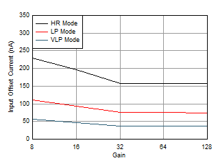
Gains of 8, 16, 32, 64, and 128 only
Figure 6-4 Input Offset Current vs Gain
GUID-20210211-CA0I-PXDJ-GZRV-SJVC16ZPR0RX-low.svg
 
Figure 6-6 Startup Time Histogram
GUID-111124E3-4E5B-4B5C-A2D6-F4E486A59A50-low.gif
 
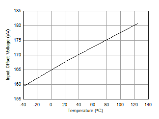
Figure 6-8 Input Offset Voltage vs Temperature
GUID-20210211-CA0I-8BHJ-R3W3-JFR39CNHJSCT-low.svg
  12 units, all channels
Figure 6-10 Long-Term Gain Drift (TQFP Package)
GUID-20210211-CA0I-ZJRL-KNQD-1Z5Z3ZJTXNNZ-low.svg
12 units, all channels 
Figure 6-12 Gain Error vs Humidity
GUID-CC971A1D-18F0-4439-B367-A4A15F5DF554-low.gif
 
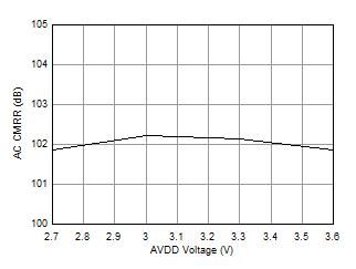
Figure 6-14 AC CMRR vs AVDD
GUID-6925A060-EF13-44AF-B43C-B81F62F11AD4-low.gif
 
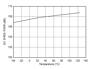
Figure 6-16 DC DVDD PSRR vs Temperature
GUID-20210211-CA0I-W7JM-29SM-CCK65ZDL9JDM-low.svg
Gain = 1, inputs shorted
Figure 6-18 Single Device Noise Histogram at 4 kSPS
GUID-2619A9A0-4379-41F7-93E6-6E059CB6AC7A-low.gif
 
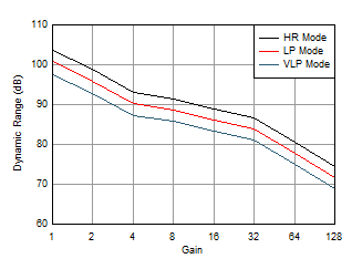
Figure 6-20 Dynamic Range vs Gain Across Power Modes
GUID-DD79F3E0-2854-451D-A1BA-09422CEC7C78-low.gif
 
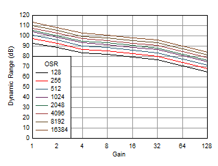
Figure 6-22 Dynamic Range vs Gain Across OSR
GUID-20210211-CA0I-S70F-D3C2-VV51TCVGXC7V-low.svg
 
Figure 6-24 THD vs Gain
GUID-20210211-CA0I-WMK2-4VX5-8PFDJZHPMTFX-low.svg
 32 units
Figure 6-26 Long-Term Reference Drift (TQFP Package)
GUID-20210211-CA0I-VX9F-RNBD-6XMX4VG4NQM4-low.svg
32 units 
Figure 6-28 Reference Error vs Humidity
GUID-7C8D4EF3-C26C-41E3-A2E0-2AF3D4080485-low.gif
 
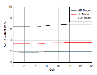
Figure 6-30 AVDD Current vs Gain
GUID-752F2E7C-356E-41E3-AA88-C919D5BBAD7F-low.gif
 
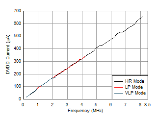
Figure 6-32 DVDD Current vs CLKIN Frequency
GUID-20210201-CA0I-PQVN-9BTN-LQKSQVFBFDBQ-low.svg
 
Figure 6-5 Input Impedance vs Gain
GUID-4A536DFE-A1CE-4246-BEC8-88FAB8B8C823-low.gif
30 units, channel 1
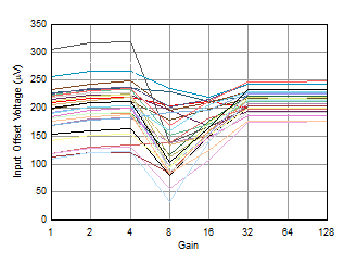
Figure 6-7 Input Offset Voltage vs Gain
GUID-20210211-CA0I-Q9X2-SNVQ-SRTVV08KB0F1-low.svg
Includes internal reference error
Figure 6-9 Gain Error vs Temperature
GUID-20210201-CA0I-FDJK-DZ75-PZDMWVX749BB-low.svg
 12 units, all channels
Figure 6-11 Long-Term Gain Drift (WQFN Package)
GUID-20210201-CA0I-8BMD-DGSV-HSWSVVB1F1QZ-low.svg
 
Figure 6-13 DC CMRR vs Temperature
GUID-FBBBEA12-49F0-433F-B21F-C98A9F692443-low.gif
 
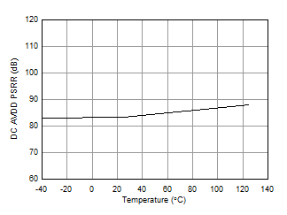
Figure 6-15 DC AVDD PSRR vs Temperature
GUID-20210201-CA0I-19XR-D4GT-S3JGQK1M7XWH-low.svg
 
Figure 6-17 Noise vs Temperature
GUID-20210211-CA0I-SGD3-RMCL-H8JSBNFNX0XX-low.svg
Gain = 1, inputs shorted
Figure 6-19 Single Device Noise Histogram at 32 kSPS
GUID-20210211-CA0I-LJML-D8ZS-CMQJDBC4ZTZ5-low.svg
 
Figure 6-21 Dynamic Range vs Gain Across Channels
GUID-FE39F033-F26A-4632-9396-52B6D18061DA-low.gif
 
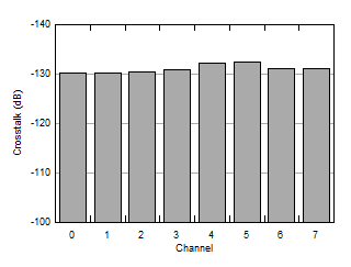
Figure 6-23 Crosstalk vs Channel
GUID-20210211-CA0I-L2QK-G29K-FNTD2TJMRZGR-low.svg
 
Figure 6-25 THD vs AVDD
GUID-20210201-CA0I-WH6M-NJ95-BZTF4WZGWCKH-low.svg
32 units 
Figure 6-27 Long-Term Reference Drift (WQFN Package)
GUID-20210201-CA0I-WGW7-T7F0-XPFRR7V6NHH6-low.svg
 
Figure 6-29 Internal Reference Voltage Temperature Drift
GUID-B3B2D44B-8F7E-4EB0-9EAF-A56A2D3212DC-low.gif
 
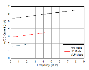
Figure 6-31 AVDD Current vs CLKIN Frequency