SBAS520C February 2011 – June 2017 ADS4122 , ADS4125 , ADS4142 , ADS4145
PRODUCTION DATA.
- 1 Features
- 2 Applications
- 3 Description
- 4 Revision History
- 5 Device Family Comparison
- 6 Pin Configuration and Functions
-
7 Specifications
- 7.1 Absolute Maximum Ratings
- 7.2 ESD Ratings
- 7.3 Recommended Operating Conditions
- 7.4 Thermal Information
- 7.5 Electrical Characteristics: ADS412x
- 7.6 Electrical Characteristics: ADS414x
- 7.7 Electrical Characteristics: General
- 7.8 Digital Characteristics
- 7.9 Timing Requirements: LVDS and CMOS Modes
- 7.10 Serial Interface Timing Characteristics
- 7.11 Reset Timing Requirements
- 7.12 Timing Characteristics at Lower Sampling Frequencies
- 7.13 Typical Characteristics: ADS4122
- 7.14 Typical Characteristics: ADS4125
- 7.15 Typical Characteristics: ADS4142
- 7.16 Typical Characteristics: ADS4145
- 7.17 Typical Characteristics: Common
- 7.18 Typical Characteristics: Contour
- 8 Detailed Description
- 9 Application and Implementation
- 10Power Supply Recommendations
- 11Layout
- 12Device and Documentation Support
- 13Mechanical, Packaging, and Orderable Information
Package Options
Mechanical Data (Package|Pins)
- RGZ|48
Thermal pad, mechanical data (Package|Pins)
- RGZ|48
Orderable Information
11 Layout
11.1 Layout Guidelines
11.1.1 Grounding
A single ground plane is sufficient to give good performance, provided the analog, digital, and clock sections of the board are cleanly partitioned. See the ADS414x, ADS412x EVM User Guide for details on layout and grounding.
11.1.2 Supply Decoupling
Because the ADS412x and ADS414x already include internal decoupling, minimal external decoupling can be used without loss in performance. Note that decoupling capacitors can help filter external power-supply noise, so the optimum number of capacitors depends on the actual application. The decoupling capacitors must be placed very close to the converter supply pins.
11.1.3 Exposed Pad
In addition to providing a path for heat dissipation, the thermal pad is also electrically internally connected to the digital ground. Therefore, solder the exposed pad to the ground plane for best thermal and electrical performance. For detailed information, see application notes, QFN Layout Guidelines (SLOA122) and QFN/SON PCB Attachment (SLUA271) that are both available for download at www.ti.com.
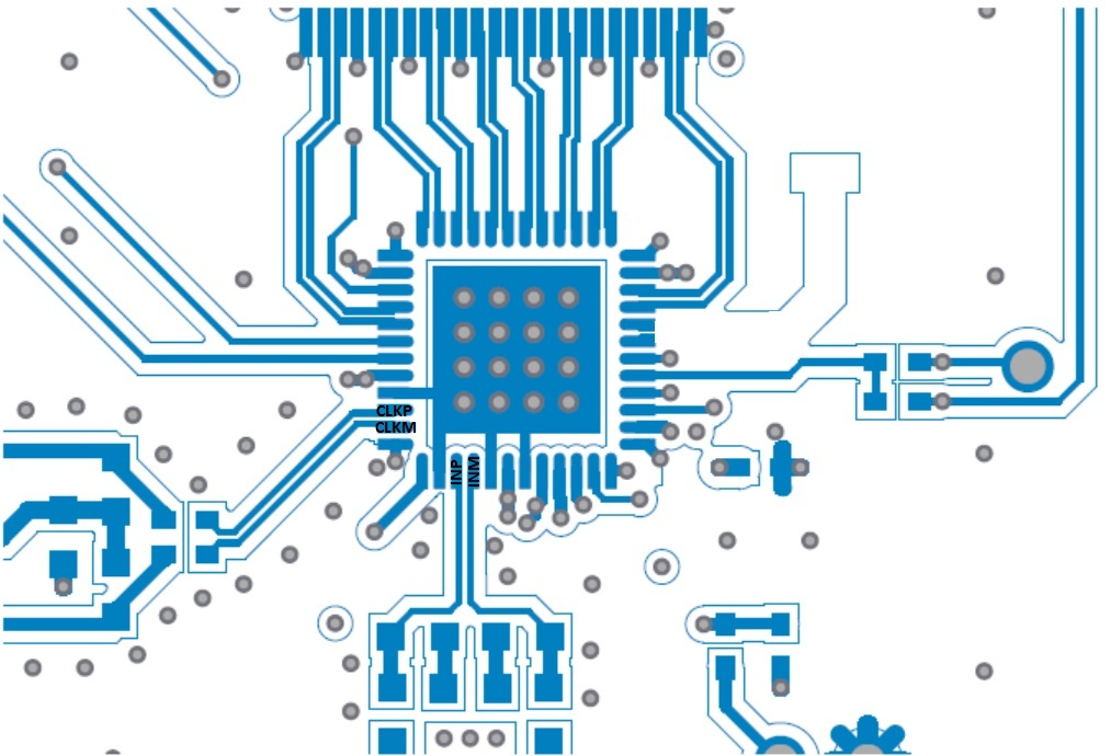
11.2 Layout Example
 Figure 165. ADS412x and ADS414x EVM PCB Layout