SBAS534E July 2011 – January 2016 ADS4249
PRODUCTION DATA.
- 1 Features
- 2 Applications
- 3 Description
- 4 Revision History
- 5 ADS424x, ADS422x Family Comparison
- 6 Pin Configuration and Functions
-
7 Specifications
- 7.1 Absolute Maximum Ratings
- 7.2 ESD Ratings
- 7.3 Recommended Operating Conditions
- 7.4 Thermal Information
- 7.5 Electrical Characteristics: ADS4249 (250 MSPS)
- 7.6 Electrical Characteristics: General
- 7.7 Digital Characteristics
- 7.8 LVDS and CMOS Modes Timing Requirements
- 7.9 LVDS Timings at Lower Sampling Frequencies
- 7.10 CMOS Timings at Lower Sampling Frequencies
- 7.11 Serial Interface Timing Characteristics
- 7.12 Reset Timing (Only when Serial Interface is Used)
- 7.13 Typical Characteristics
-
8 Detailed Description
- 8.1 Overview
- 8.2 Functional Block Diagram
- 8.3 Feature Description
- 8.4 Device Functional Modes
- 8.5 Programming
- 8.6
Register Maps
- 8.6.1 Serial Register Map
- 8.6.2
Description of Serial Registers
- 8.6.2.1 Register Address 00h (Default = 00h)
- 8.6.2.2 Register Address 01h (Default = 00h)
- 8.6.2.3 Register Address 01h (Default = 00h)
- 8.6.2.4 Register Address 25h (Default = 00h)
- 8.6.2.5 Register Address 29h (Default = 00h)
- 8.6.2.6 Register Address 2Bh (Default = 00h)
- 8.6.2.7 Register Address 3Dh (Default = 00h)
- 8.6.2.8 Register Address 3Fh (Default = 00h)
- 8.6.2.9 Register Address 40h (Default = 00h)
- 8.6.2.10 Register Address 41h (Default = 00h)
- 8.6.2.11 Register Address 42h (Default = 00h)
- 8.6.2.12 Register Address 45h (Default = 00h)
- 8.6.2.13 Register Address 4Ah (Default = 00h)
- 8.6.2.14 Register Address 58h (Default = 00h)
- 8.6.2.15 Register Address BFh (Default = 00h)
- 8.6.2.16 Register Address C1h (Default = 00h)
- 8.6.2.17 Register Address CFh (Default = 00h)
- 8.6.2.18 Register Address EFh (Default = 00h)
- 8.6.2.19 Register Address F1h (Default = 00h)
- 8.6.2.20 Register Address F2h (Default = 00h)
- 8.6.2.21 Register Address 2h (Default = 00h)
- 8.6.2.22 Register Address D5h (Default = 00h)
- 8.6.2.23 Register Address D7h (Default = 00h)
- 8.6.2.24 Register Address DBh (Default = 00h)
- 9 Application and Implementation
- 10Power Supply Recommendations
- 11Layout
- 12Device and Documentation Support
- 13Mechanical, Packaging, and Orderable Information
Package Options
Mechanical Data (Package|Pins)
- RGC|64
Thermal pad, mechanical data (Package|Pins)
- RGC|64
Orderable Information
11 Layout
11.1 Layout Guidelines
11.1.1 Grounding
A single ground plane is sufficient to give good performance, provided the analog, digital, and clock sections of the board are cleanly partitioned. See the ADS4226 Evaluation Module (SLAU333) for details on layout and grounding.
11.1.2 Exposed Pad
In addition to providing a path for heat dissipation, the PowerPAD is also electrically connected internally to the digital ground. Therefore, the exposed pad must be soldered to the ground plane for best thermal and electrical performance. For detailed information, see application notes QFN Layout Guidelines (SLOA122) and QFN/SON PCB Attachment (SLUA271).
11.1.3 Routing Analog Inputs
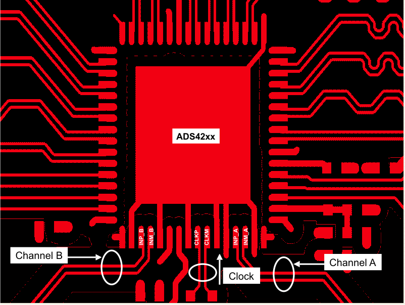
Routing differential analog input pairs (INP_x and INM_x) close to each other is advisable. To minimize the possibility of coupling from a channel analog input to the sampling clock, the analog input pairs of both channels must be routed perpendicular to the sampling clock; see the ADS4226 Evaluation Module (SLAU333) for reference routing. Figure 85 illustrates a snapshot of the PCB layout from the ADS42xxEVM.
11.1.4 Routing Digital Inputs
The digital outputs must be routed away from the analog inputs and any noise sensitive circuits. Avoid routing the digital outputs in parallel to any analog trace. The digital outputs must be routed over a solid ground plane all the way to the FPGA. Keep the digital traces as short as possible to reduce EMI emissions. The traces must be matched length to maintain timing, however mismatches in the trace lengths can be taken into account by including the delay differences in the FPGA timing constraints.
11.2 Layout Example
 Figure 85. ADS42xxEVM PCB Layout