SBAS773A September 2017 – December 2017 ADS7142
PRODUCTION DATA.
- 1 Features
- 2 Applications
- 3 Description
- 4 Revision History
- 5 Pin Configuration and Functions
-
6 Specifications
- 6.1 Absolute Maximum Ratings
- 6.2 ESD Ratings
- 6.3 Recommended Operating Conditions
- 6.4 Thermal Information
- 6.5 Electrical Characteristics - All Modes
- 6.6 Electrical Characteristics - Manual Mode
- 6.7 Electrical Characteristics - Autonomous Modes
- 6.8 Electrical Characteristics - High Precision Mode
- 6.9 Timing Requirements
- 6.10 Switching Characteristics
- 6.11 Typical Characteristics for All Modes
- 6.12 Typical Characteristics for Manual Mode
- 6.13 Typical Characteristics for Autonomous Modes
- 6.14 Typical Characteristics for High Precision Mode
-
7 Detailed Description
- 7.1 Overview
- 7.2 Functional Block Diagram
- 7.3 Feature Description
- 7.4 Device Functional Modes
- 7.5 Optimizing Power Consumed by the Device
- 7.6
Register Map
- 7.6.1 RESET REGISTERS
- 7.6.2 FUNCTIONAL MODE SELECT REGISTERS
- 7.6.3 INPUT CONFIG REGISTER
- 7.6.4 ANALOG MUX and SEQUENCER REGISTERS
- 7.6.5 OSCILLATOR and TIMING CONTROL REGISTERS
- 7.6.6 DATA BUFFER CONTROL REGISTER
- 7.6.7
ACCUMULATOR CONTROL REGISTERS
- 7.6.7.1 ACC_EN Register (address = 30h), [reset = 00h]
- 7.6.7.2 ACC_CH0_LSB Register (address = 08h), [reset = 00h]
- 7.6.7.3 ACC_CH0_MSB Register (address = 09h), [reset = 00h]
- 7.6.7.4 ACC_CH1_LSB Register (address = 0Ah), [reset = 00h]
- 7.6.7.5 ACC_CH1_MSB Register (address = 0Bh), [reset = 00h]
- 7.6.7.6 ACCUMULATOR_STATUS Register (address = 02h), [reset = 00h]
- 7.6.8
DIGITAL WINDOW COMPARATOR REGISTERS
- 7.6.8.1 ALERT_DWC_EN Register (address = 37h), [reset = 00h]
- 7.6.8.2 ALERT_CHEN (address = 34h), [reset = 00h]
- 7.6.8.3 DWC_HTH_CH0_MSB Register (address = 39h), [reset = 00h]
- 7.6.8.4 DWC_HTH_CH0_LSB Register (address = 38h), [reset = 00h]
- 7.6.8.5 DWC_LTH_CH0_MSB Register (address = 3Bh), [reset = 00h]
- 7.6.8.6 DWC_LTH_CH0_LSB Register (address = 3Ah), [reset = 00h]
- 7.6.8.7 DWC_HYS_CH0 (address = 40h), [reset = 00h]
- 7.6.8.8 DWC_HTH_CH1_MSB Register (address = 3Dh), [reset = 00h]
- 7.6.8.9 DWC_HTH_CH1_LSB Register (address = 3Ch), [reset = 00h]
- 7.6.8.10 DWC_LTH_CH1_MSB Register (address = 3Fh), [reset = 00h]
- 7.6.8.11 DWC_LTH_CH1_LSB Register (address = 3Eh), [reset = 00h]
- 7.6.8.12 DWC_HYS_CH1 (address = 41h), [reset = 00h]
- 7.6.8.13 PRE_ALT_MAX_EVENT_COUNT Register (address = 36h), [reset = 00h]
- 7.6.8.14 ALERT_TRIG_CHID Register (address = 03h), [reset = 00h]
- 7.6.8.15 ALERT_LOW_FLAGS Register (address = 0C), [reset = 00h]
- 7.6.8.16 ALERT_HIGH_FLAGS Register (address = 0Eh), [reset = 00h]
- 8 Application and Implementation
- 9 Power-Supply Recommendations
- 10Layout
- 11Device and Documentation Support
- 12Mechanical, Packaging, and Orderable Information
Package Options
Mechanical Data (Package|Pins)
- RUG|10
Thermal pad, mechanical data (Package|Pins)
- RUG|10
Orderable Information
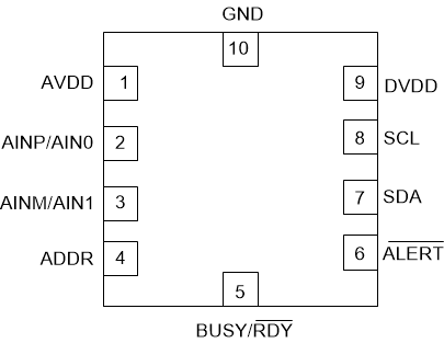
5 Pin Configuration and Functions
RUG PACKAGE
10-Pin X2QFN
TOP VIEW

Pin Functions
| PIN | I/O | DESCRIPTION | |
|---|---|---|---|
| NAME | NO. | ||
| AVDD | 1 | Supply | Analog supply input, also used as the reference voltage for analog-to-digital conversion. |
| AINP/AIN0 | 2 | Analog input | Single-Channel operation: Positive analog signal input Two-Channel operation: Analog signal input, Channel 0 |
| AINM/AIN1 | 3 | Analog input | Single-Channel operation: Negative analog signal input Two-Channel operation: Analog signal input, Channel 1 |
| ADDR | 4 | Analog Input | Input for selecting I2C address of the device. The device address can be selected from one of the eight values by connecting resistors on this pin. Refer Table 2 for details |
| BUSY/RDY | 5 | Digital output | The device pulls this pin high when it is scanning through channels in a sequence and brings this pin low when sequence is completed or aborted. |
| ALERT | 6 | Digital output | Active low, open drain output. Status of this pin is controlled by Digital window comparator block. Connect a pull-up resistor from DVDD to this pin |
| SDA | 7 | Digital input/output | Serial data in/out for I2C interface. Connect a pull-up resistor from DVDD to this pin |
| SCL | 8 | Digital input | Serial clock for I2C interface. Connect a pull-up resistor from DVDD to this pin |
| DVDD | 9 | Supply | Digital I/O supply voltage |
| GND | 10 | Supply | Ground for power supply, all analog and digital signals are referred to this pin |