SBAS773A September 2017 – December 2017 ADS7142
PRODUCTION DATA.
- 1 Features
- 2 Applications
- 3 Description
- 4 Revision History
- 5 Pin Configuration and Functions
-
6 Specifications
- 6.1 Absolute Maximum Ratings
- 6.2 ESD Ratings
- 6.3 Recommended Operating Conditions
- 6.4 Thermal Information
- 6.5 Electrical Characteristics - All Modes
- 6.6 Electrical Characteristics - Manual Mode
- 6.7 Electrical Characteristics - Autonomous Modes
- 6.8 Electrical Characteristics - High Precision Mode
- 6.9 Timing Requirements
- 6.10 Switching Characteristics
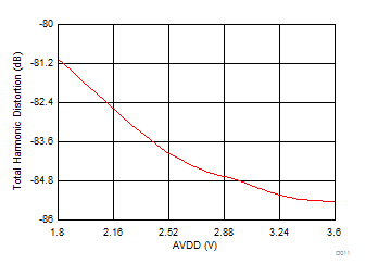
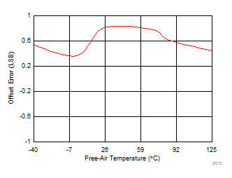
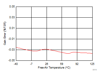
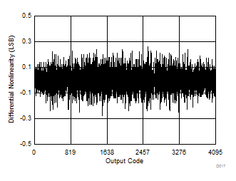
- 6.11 Typical Characteristics for All Modes
- 6.12 Typical Characteristics for Manual Mode
- 6.13 Typical Characteristics for Autonomous Modes
- 6.14 Typical Characteristics for High Precision Mode
-
7 Detailed Description
- 7.1 Overview
- 7.2 Functional Block Diagram
- 7.3 Feature Description
- 7.4 Device Functional Modes
- 7.5 Optimizing Power Consumed by the Device
- 7.6
Register Map
- 7.6.1 RESET REGISTERS
- 7.6.2 FUNCTIONAL MODE SELECT REGISTERS
- 7.6.3 INPUT CONFIG REGISTER
- 7.6.4 ANALOG MUX and SEQUENCER REGISTERS
- 7.6.5 OSCILLATOR and TIMING CONTROL REGISTERS
- 7.6.6 DATA BUFFER CONTROL REGISTER
- 7.6.7
ACCUMULATOR CONTROL REGISTERS
- 7.6.7.1 ACC_EN Register (address = 30h), [reset = 00h]
- 7.6.7.2 ACC_CH0_LSB Register (address = 08h), [reset = 00h]
- 7.6.7.3 ACC_CH0_MSB Register (address = 09h), [reset = 00h]
- 7.6.7.4 ACC_CH1_LSB Register (address = 0Ah), [reset = 00h]
- 7.6.7.5 ACC_CH1_MSB Register (address = 0Bh), [reset = 00h]
- 7.6.7.6 ACCUMULATOR_STATUS Register (address = 02h), [reset = 00h]
- 7.6.8
DIGITAL WINDOW COMPARATOR REGISTERS
- 7.6.8.1 ALERT_DWC_EN Register (address = 37h), [reset = 00h]
- 7.6.8.2 ALERT_CHEN (address = 34h), [reset = 00h]
- 7.6.8.3 DWC_HTH_CH0_MSB Register (address = 39h), [reset = 00h]
- 7.6.8.4 DWC_HTH_CH0_LSB Register (address = 38h), [reset = 00h]
- 7.6.8.5 DWC_LTH_CH0_MSB Register (address = 3Bh), [reset = 00h]
- 7.6.8.6 DWC_LTH_CH0_LSB Register (address = 3Ah), [reset = 00h]
- 7.6.8.7 DWC_HYS_CH0 (address = 40h), [reset = 00h]
- 7.6.8.8 DWC_HTH_CH1_MSB Register (address = 3Dh), [reset = 00h]
- 7.6.8.9 DWC_HTH_CH1_LSB Register (address = 3Ch), [reset = 00h]
- 7.6.8.10 DWC_LTH_CH1_MSB Register (address = 3Fh), [reset = 00h]
- 7.6.8.11 DWC_LTH_CH1_LSB Register (address = 3Eh), [reset = 00h]
- 7.6.8.12 DWC_HYS_CH1 (address = 41h), [reset = 00h]
- 7.6.8.13 PRE_ALT_MAX_EVENT_COUNT Register (address = 36h), [reset = 00h]
- 7.6.8.14 ALERT_TRIG_CHID Register (address = 03h), [reset = 00h]
- 7.6.8.15 ALERT_LOW_FLAGS Register (address = 0C), [reset = 00h]
- 7.6.8.16 ALERT_HIGH_FLAGS Register (address = 0Eh), [reset = 00h]
- 8 Application and Implementation
- 9 Power-Supply Recommendations
- 10Layout
- 11Device and Documentation Support
- 12Mechanical, Packaging, and Orderable Information
Package Options
Mechanical Data (Package|Pins)
- RUG|10
Thermal pad, mechanical data (Package|Pins)
- RUG|10
Orderable Information
6 Specifications
6.1 Absolute Maximum Ratings
over operating free-air temperature range (unless otherwise noted)(1)| MIN | MAX | UNIT | |
|---|---|---|---|
| ADDR to GND | –0.3 | AVDD + 0.3 | V |
| AVDD to GND | –0.3 | 3.9 | V |
| DVDD to GND | –0.3 | 3.9 | V |
| AINP/AIN0 to GND | –0.3 | AVDD + 0.3 | V |
| AINM/AIN1 to GND | –0.3 | AVDD + 0.3 | V |
| Input current on any pin except supply pins | -10 | 10 | mA |
| Digital Input to GND | –0.3 | DVDD + 0.3 | V |
| Storage Temperature, Tstg | –60 | 150 | °C |
6.2 ESD Ratings
| VALUE | UNIT | |||
|---|---|---|---|---|
| V(ESD) | Electrostatic discharge | Human body model (HBM), per ANSI/ESDA/JEDEC JS-001, all pins(1) | ±2000 | V |
| Charged device model (CDM), per JEDEC specification JESD22-C101, all pins(2) | ±1000 | |||
6.3 Recommended Operating Conditions
over operating free-air temperature range (unless otherwise noted)| MIN | NOM | MAX | UNIT | ||
|---|---|---|---|---|---|
| AVDD | Analog Supply Voltage Range | 1.65 | 3.6 | V | |
| DVDD | Digital Voltage Supply Voltage Range | 1.65 | 3.6 | A | |
| TA | Ambient temperature | –40 | 125 | °C | |
| TJ | Junction temperature | –60 | 150 | °C | |
6.4 Thermal Information
| THERMAL METRIC(1) | ADS7142 | UNIT | |
|---|---|---|---|
| RUG | |||
| 10 PINS | |||
| RθJA | Junction-to-ambient thermal resistance | 120.3 | °C/W |
| RθJC(top) | Junction-to-case (top) thermal resistance | 42.7 | °C/W |
| RθJB | Junction-to-board thermal resistance | 51.1 | °C/W |
| ΨJT | Junction-to-top characterization parameter | 0.8 | °C/W |
| ΨJB | Junction-to-board characterization parameter | 51.2 | °C/W |
| RθJC(bot) | Junction-to-case (bottom) thermal resistance | N/A | °C/W |
6.5 Electrical Characteristics - All Modes
At TA = -40°C to 125°C, AVDD = 3V, DVDD = 1.65 to 3.6V, All Channel Configurations, unless otherwise noted.| PARAMETER | TEST CONDITIONS | MIN | TYP | MAX | UNIT | |
|---|---|---|---|---|---|---|
| ANALOG INPUT - Two-Channel Single-Ended Configuration | ||||||
| Full-scale input voltage span(1) | AINP/AIN0 to GND or AINM/AIN1 to GND | 0 | AVDD | V | ||
| Absoulte Input voltage range | AINP/AIN0 to GND or AINM/AIN1 to GND | –0.1 | AVDD + 0.1 | V | ||
| ANALOG INPUT - Single-Channel Single-Ended Configuration (with Remote Ground Sense) | ||||||
| Full-scale input voltage span(1) | AINP/AIN0 to GND or AINM/AIN1 to GND | 0 | AVDD | V | ||
| Absoulte Input voltage range | AINP/AIN0 to GND | –0.1 | AVDD + 0.1 | V | ||
| AINM/AIN1 to GND | –0.1 | 0.1 | V | |||
| ANALOG INPUT - Single-Channel Pseudo-Differential Configuration | ||||||
| Full-scale input voltage span(1) | AINP/AIN0 to GND or AINM/AIN1 to GND | –AVDD/2 | AVDD/2 | V | ||
| Absoulte Input voltage range | AINP/AIN0 to GND | –0.1 | AVDD + 0.1 | V | ||
| AINM/AIN1 to GND | AVDD/2–0.1 | AVDD/2+0.1 | V | |||
| Internal Oscillator | ||||||
| tHSO | Time Period for High Speed Oscillator | 50 | 110 | ns | ||
| tLPO | Time Period for Low Power Oscillator | 95.2 | 300 | µs | ||
| Digital Input/Output (SCL, SDA) | ||||||
| VIH | High Level input Voltage | 0.7 × DVDD | DVDD | V | ||
| VIL | Low Level input Voltage | 0 | 0.3 × DVDD | V | ||
| VOL | Low Level output Voltage | With 3 mA Sink Current and DVDD > 2 V | 0 | 0.4 | V | |
| With 3 mA Sink Current and 1.65 V < DVDD < 2 V | 0 | 0.2 × DVDD | V | |||
| IOL | Low Level Output Current (Sink) | VOL = 0.4 V for Standard and Fast Mode (100, 400 kHz) | 3 | mA | ||
| VOL = 0.6 V for Fast Mode (400 kHz) | 6 | |||||
| VOL = 0.4 V Fast Mode Plus (1 MHz) | 20 | |||||
| IOL | Low Level Output Current (Sink) | VOL= 0.4 V High Speed (1.7 MHz, 3.4 MHz) | 25 | mA | ||
| II | Input Current on Pin | 10 | µA | |||
| CI | Input Capacitance on Pin | 10 | pF | |||
| Digital Output (BUSY/RDY) | ||||||
| VOH | High Level Output Voltage | Isource = 2 mA | 0.7 × DVDD | DVDD | V | |
| VOL | High Level Output Voltage | Isink = 2 mA | 0 | 0.3 × DVDD | V | |
| Digital Output (ALERT) | ||||||
| IOL | Low Level Output Current | VOL < 0.25 V | 5 | mA | ||
| VOL | Low Level Output Voltage | Isink = 5 mA | 0 | 0.25 | V | |
| POWER-SUPPLY REQUIREMENTS | ||||||
| AVDD | Analog Supply Voltage | 1.65 | 3.6 | V | ||
| DVDD | Digital I/O Suplly Voltage | 1.65 | 3.6 | V | ||
6.6 Electrical Characteristics - Manual Mode
At TA = -40°C to 125°C, AVDD = 3V, DVDD = 1.65 to 3.6V, All Channel Configurations, unless otherwise noted.| PARAMETER | TEST CONDITIONS | MIN | TYP | MAX | UNIT | |
|---|---|---|---|---|---|---|
| Sampling Dynamics | ||||||
| tconv | Conversion Time | AVDD = 1.65 to 3.6V | 1.8 | µs | ||
| tacq | Acquistion Time | AVDD = 1.65 to 3.6V | 18 | TSCL | ||
| tcycle | Cycle Time | AVDD = 1.65 to 3.6V | (tconv + tacq) | µs | ||
| DC Specifications | ||||||
| Resolution | 12 | Bits | ||||
| NMC | No Missing Codes | AVDD = 1.65 to 3.6V | 12 | Bits | ||
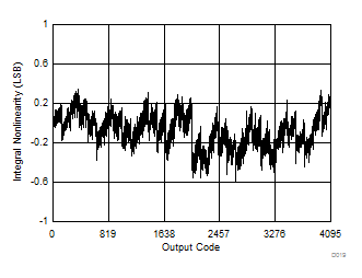
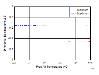
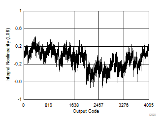
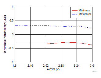
| DNL | Differential nonlinerity | AVDD = 1.65 to 3.6V | –0.99 | ±0.3 | 1 | LSB(1) |
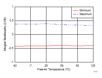
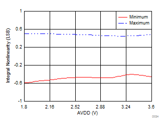
| INL | Integral nonlinearity | –2.75 | ±0.5 | 2.75 | LSB | |
| EO | Offset Error | Post Offset Calibration | –2.9 | ±0.5 | 2.9 | LSB |
| dVOS/dT | Offset Drift with Temperature | Post Offset Calibration | 5 | ppm/°C | ||
| EG | Gain Error | –0.1 | ±0.03 | 0.1 | %FSR | |
| Gain Error Drift with Temperature | 5 | ppm/°C | ||||
| AC Specifications | ||||||
| SNR(2) | Signal-to-Noise Ratio | fin = 2 kHz, AVDD = 3 V, fsample =140 kSPS | 68.75 | 71.4 | dB | |
| fin = 2 kHz, AVDD = 1.8 V, fsample =140 kSPS | 69.2 | dB | ||||
| THD(2) (3) | Total Harmonic Distortion | fin = 2 kHz, AVDD = 3 V, fsample =140 kSPS | –87.0 | dB | ||
| fin = 2 kHz, AVDD = 1.8 V, fsample =140 kSPS | –84.0 | dB | ||||
| SINAD(2) | Signal-to-Noise and distortion | fin = 2 kHz, AVDD = 3 V, fsample =140 kSPS | 68.5 | 71.2 | dB | |
| fin = 2 kHz, AVDD = 1.8 V, fsample =140 kSPS | 69.0 | dB | ||||
| SFDR(2) | Spurious Free dynamic range | fin = 2 kHz, AVDD = 3 V, fsample =140 kSPS | 91.0 | dB | ||
| BW | -3dB Small Signal Bandwidth | 25.0 | MHz | |||
| Power Consumption | ||||||
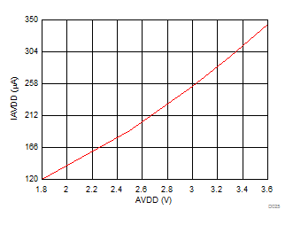
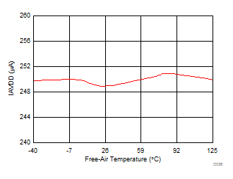
| IAVDD | Analog Supply Current | fsample =140 kSPS, SCL = 3.4 MHz | 265 | 300 | µA | |
| fsample =5.5 kSPS, SCL = 100 kHz | 8 | µA | ||||
| fsample =140 kSPS, SCL = 3.4 MHz, AVDD = 1.8 V | 160 | µA | ||||
| fsample =5.5 kSPS, SCL = 100 kHz, AVDD = 1.8 V | 5 | µA | ||||
| IDVDD | Digital Supply Current | fsample =140 kSPS, SCL = 3.4 MHz, SDA = AAA0h | 25 | µA | ||
| fsample =5.5 kSPS, SCL = 100 kHz, AVDD = 1.8 V, SDA = AAA0h | 1.5 | µA | ||||
| IAVDD | Static Analog Supply Current | No Activity on SCL and SDA, BUSY/RDY Low | 6 | nA | ||
| IDVDD | Static Analog Supply Current | No Activity on SCL and SDA, BUSY/RDY Low | 2 | nA | ||
6.7 Electrical Characteristics - Autonomous Modes
At TA = -40°C to 125°C, AVDD = 3V, DVDD = 1.65 to 3.6V, All Channel Configurations, unless otherwise noted.| PARAMETER | TEST CONDITIONS | MIN | TYP | MAX | UNIT | |
|---|---|---|---|---|---|---|
| Sampling Dynamics | ||||||
| tconv | Conversion Time | High Speed Oscillator | 14 | tHSO | ||
| Low Power Oscillator | 14 | tLPO | ||||
| tacq | Acquistion Time | High Speed Oscillator | 7 | tHSO | ||
| Low Power Oscillator | 4 | tLPO | ||||
| tcycle | Cycle Time | High Speed Oscillator | nCLK | tHSO | ||
| Low Power Oscillator | nCLK | tLPO | ||||
| DC Specifications | ||||||
| Resolution | 12 | Bits | ||||
| EO | Offset Error | Post Offset Calibration | ±0.5 | LSB | ||
| EG | Gain Error | ±0.03 | %FSR | |||
| Power Consumption | ||||||
| IAVDD | Analog Supply Current | With Low Power Oscillator, nCLK =18 | 0.75 | µA | ||
| With Low Power Oscillator, AVDD = 1.8 V, nCLK =18 | 0.45 | µA | ||||
| With Low Power Oscillator, nCLK = 250 | 0.5 | µA | ||||
| With High Speed Oscillator, nCLK =21 | 940 | µA | ||||
| IDVDD | Digital Supply Current | With Low Power Oscillator, nCLK =18, DVDD =3.3 V | 0.15 | µA | ||
| IAVDD | Static Analog Supply Current | No Activity on SCL and SDA, BUSY/RDY Low | 5 | nA | ||
| IDVDD | Static Analog Supply Current | No Activity on SCL and SDA, BUSY/RDY Low | 0.6 | nA | ||
6.8 Electrical Characteristics - High Precision Mode
At TA = -40°C to 125°C, AVDD = 3V, DVDD = 1.65 to 3.6V, All Channel Configurations, unless otherwise noted(1).| PARAMETER | TEST CONDITIONS | MIN | TYP | MAX | UNIT | |
|---|---|---|---|---|---|---|
| DC Specifications | ||||||
| Resolution(2) | 16 | Bits | ||||
| ENOB | Effective number of bits | With DC Input of AVDD/2(3) | 15.4 | |||
| EO | Offset Error | Post Offset Calibration | ±10 | LSB | ||
| EG | Gain Error | ±0.03 | %FSR | |||
| Power Consumption | ||||||
| IAVDD | Analog Supply Current | With Low Power Oscillator, nCLK =18 | 0.6 | µA | ||
| With Low Power Oscillator, AVDD = 1.8 V, nCLK =18 | 0.3 | µA | ||||
| With Low Power Oscillator, nCLK = 250 | 0.5 | µA | ||||
| With High Speed Oscillator, nCLK =21 | 980 | µA | ||||
| IDVDD | Digital Supply Current | With Low Power Oscillator, nCLK =21, DVDD =3.3 V | 0.2 | µA | ||
| IAVDD | Static Analog Supply Current | No Activity on SCL and SDA, BUSY/RDY Low | 5 | nA | ||
| IDVDD | Static Analog Supply Current | No Activity on SCL and SDA, BUSY/RDY Low | 0.7 | nA | ||
6.9 Timing Requirements
At TA = -40°C to 125°C, AVDD = 3V, DVDD = 1.65 to 3.6V, All Channel Configurations, unless otherwise noted.(1)| PARAMETER | Test Conditions | MIN | MAX | UNIT | |
|---|---|---|---|---|---|
| Standard-mode (100 kHz) Figure 1 | |||||
| fSCL | SCL clock frequency | 0 | 100 | kHz | |
| tHD-STA | Hold time (repeated) START condition | After this period, the first clock pulse generated. | 4 | µs | |
| tLOW | Low period of SCL | 4.7 | µs | ||
| tHIGH | High period of SCL | 4 | µs | ||
| tSU-STA | set-up time for a repeated start condition | 4.7 | µs | ||
| tHD-DAT (2) (3) | data hold time | For I2C Bus devices | 0 | µs | |
| tSU-DAT | data setup time | 250 | ns | ||
| tSU-STO | setup-up time for STOP condition | 4 | µs | ||
| tBUF | bus free time between a STOP and START condition | 4.7 | µs | ||
| Cb | capacitive load on each line | 400 | pF | ||
| Fast-mode (400 kHz) Figure 1 | |||||
| fSCL | SCL clock frequency | 0 | 400 | kHz | |
| tHD-STA | Hold time (repeated) START condition | 0.6 | µs | ||
| tLOW | Low period of SCL | 1.3 | µs | ||
| tHIGH | High period of SCL | 0.6 | µs | ||
| tSU-STA | set-up time for a repeated start condition | 0.6 | µs | ||
| tHD-DAT | data hold time | 0 | µs | ||
| tSU-DAT | data setup time | 100 | ns | ||
| tSU-STO | setup-up time for STOP condition | 0.6 | µs | ||
| tBUF | bus free time between a STOP and START condition | 1.3 | µs | ||
| Cb | capacitive load on each line | 400 | pF | ||
| Fast-mode Plus (1000 kHz) Figure 1 | |||||
| fSCL | SCL clock frequency | 0 | 1000 | kHz | |
| tHD-STA | Hold time (repeated) START condition | 0.26 | µs | ||
| tLOW | Low period of SCL | 0.5 | µs | ||
| tHIGH | High period of SCL | 0.26 | µs | ||
| tSU-STA | set-up time for a repeated start condition | 0.26 | µs | ||
| tHD-DAT | data hold time | 0 | µs | ||
| tSU-DAT | data setup time | 50 | ns | ||
| tSU-STO | setup-up time for STOP condition | 0.26 | µs | ||
| tBUF | bus free time between a STOP and START condition | 0.5 | µs | ||
| Cb | capacitive load on each line | 550 | pF | ||
| High Speed mode (1.7 MHz) Cb = 400 pF (Max) Figure 2 | |||||
| fSCLH | SCLH clock frequency | 0 | 1.7 | MHz | |
| tHD-STA | Hold time (repeated) START condition | 160 | ns | ||
| tLOW | Low period of SCL | 320 | ns | ||
| tHIGH | High period of SCL | 120 | ns | ||
| tSU-STA | set-up time for a repeated start condition | 160 | ns | ||
| tHD-DAT | data hold time | 0 | 150 | ns | |
| tSU-DAT | data setup time | 10 | ns | ||
| tSU-STO | setup-up time for STOP condition | 160 | ns | ||
| Cb | capacitive load on each line | 400 | pF | ||
| High Speed mode (3.4 MHz) Cb = 100 pF (Max) Figure 2 | |||||
| fSCLH | SCLH clock frequency | 0 | 3.4 | MHz | |
| tHD-STA | Hold time (repeated) START condition | 160 | ns | ||
| tLOW | Low period of SCL | 160 | ns | ||
| tHIGH | High period of SCL | 60 | ns | ||
| tSU-STA | set-up time for a repeated start condition | 160 | ns | ||
| tHD-DAT | data hold time | 0 | 70 | ns | |
| tSU-DAT | data setup time | 10 | ns | ||
| tSU-STO | setup-up time for STOP condition | 160 | ns | ||
| Cb | capacitive load on each line | 100 | pF | ||
6.10 Switching Characteristics
At TA = -40°C to 125°C, AVDD = 3V, DVDD = 1.65 to 3.6V, All Channel Configurations, unless otherwise noted.(1)| PARAMETER | Test Conditions | MIN | MAX | UNIT | |
|---|---|---|---|---|---|
| Standard-mode (100 kHz) Figure 1 | |||||
| trCL | Rise time of SCL | 1000 | ns | ||
| trDA | Rise time of SDA | 1000 | ns | ||
| tfCL | Fall time of SCL | 300 | ns | ||
| tfDA | Fall time of SDA | 300 | ns | ||
| tVD-DAT (2) | data valid time | 3.45 | µs | ||
| tVD-ACK (2) | data hold time | 3.45 | µs | ||
| Fast-mode (400 kHz) Figure 1 | |||||
| trCL | Rise time of SCL | 20 | 300 | ns | |
| trDA | Rise time of SDA | 20 | 300 | ns | |
| tfCL | Fall time of SCL | 20 × DVDD/3.6 | 300 | ns | |
| tfDA | Fall time of SDA | 20 × DVDD/3.6 | 300 | ns | |
| tVD-DAT | data valid time | 0.9 | µs | ||
| tVD-ACK | data hold time | 0.9 | µs | ||
| tSP (3) | pulse width of spikes suppressed by the input filter | 0 | 50 | ns | |
| Fast-mode Pus (1000 kHz) Figure 1 | |||||
| trCL | Rise time of SCL | 120 | ns | ||
| trDA | Rise time of SDA | 120 | ns | ||
| tfCL | Fall time of SCL | 20 × DVDD/3.6 | 120 | ns | |
| tfDA | Fall time of SDA | 20 × DVDD/3.6 | 120 | ns | |
| tVD-DAT | data valid time | 0.45 | µs | ||
| tVD-ACK | data hold time | 0.45 | µs | ||
| tSP | pulse width of spikes suppressed by the input filter | 0 | 50 | ns | |
| High Speed mode (1.7 MHz) Cb = 400 pF (Max) Figure 2 | |||||
| trCL | Rise time of SCLH | 20 | 80 | ns | |
| trCL1 | Rise time of SCLH after a repeated start condition and after an acknowledge bit | 20 | 160 | ns | |
| trDA | Rise time of SDAH | 20 | 160 | ns | |
| tfCL | Fall time of SCLH | 20 | 80 | ns | |
| tfDA | Fall time of SDAH | 20 | 160 | ns | |
| tSP | pulse width of spikes suppressed by the input filter | 0 | 10 | ns | |
| High Speed mode (3.4 MHz) Cb = 100 pF (Max) Figure 2 | |||||
| trCL | Rise time of SCLH | 10 | 40 | ns | |
| trCL1 | Rise time of SCLH after a repeated start condition and after an acknowledge bit | 10 | 80 | ns | |
| trDA | Rise time of SDAH | 10 | 80 | ns | |
| tfCL | Fall time of SCLH | 10 | 40 | ns | |
| tfDA | Fall time of SDAH | 10 | 80 | ns | |
| tSP | pulse width of spikes suppressed by the input filter | 0 | 10 | ns | |
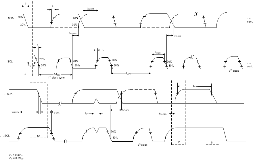 Figure 1. Timing Diagram for Standard-mode, Fast-mode and Fast-mode Plus
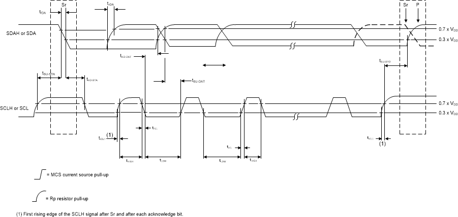 Figure 2. Timing Diagram for High Speed Mode
6.11 Typical Characteristics for All Modes
At TA = 25°C, AVDD = 3 V, DVDD = 3.3 V, and Two-Channel, Single-Ended Configuration, unless otherwise noted.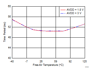
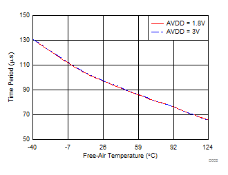
6.12 Typical Characteristics for Manual Mode
At TA = 25°C, AVDD = 3 V, DVDD = 3.3 V, and Two-Channel, Single-Ended Configuration, unless otherwise noted.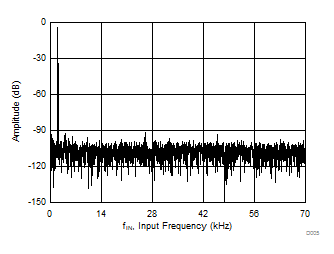
| SNR = 69.6 dB | THD = -82.9 dB | ENOB = 11.2 |
| fsample = 140 kSPS | SFDR = 87.2 dB | AVDD = 1.8 V |
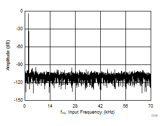
| SNR = 71.7 dB | THD = -85 dB | ENOB = 11.5 |
| fsample = 140 kSPS | SFDR = 89.2 dB | AVDD = 3 V |
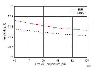
| fsample = 140 kSPS |
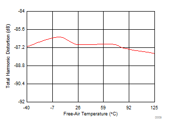
| fsample = 140 kSPS |
| fsample = 140 kSPS | S |
| AVDD = 3 V |
| AVDD = 3 V |
| fSample = 140 kSPS | SCL = 3.4 MHz |
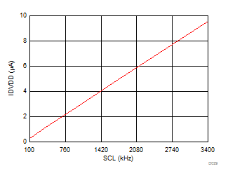
| DVDD = 1.8 V |
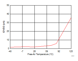
| No Activity on SCL and SDA | ||
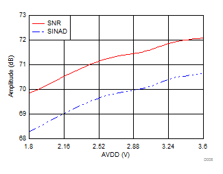
| fsample = 140 kSPS |
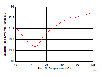
| fsample = 140 kSPS |
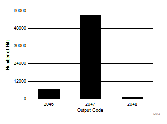
| Mean code = 2046.9 | Standard Deviation = 0.34 |
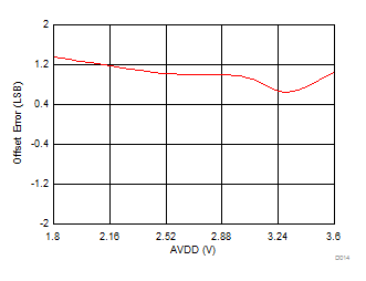
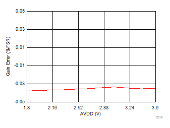
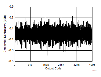
| AVDD = 1.8 V |
| AVDD = 1.8 V |
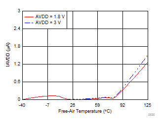
| No Activity on SCL and SDA | ||
6.13 Typical Characteristics for Autonomous Modes
At TA = 25°C, AVDD = 3 V, DVDD = 3.3 V, and Two-Channel, Single-Ended Configuration, unless otherwise noted.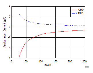
| Input Voltage = 1.5 V | With High Speed Oscillator | |
| Stop Burst Mode | ||
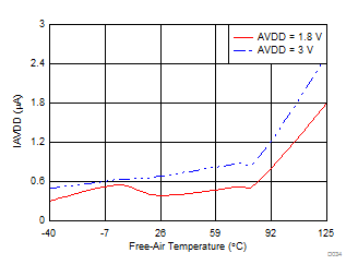
| Stop Burst Mode | With Low Power Oscillator | |
| nCLK = 25 |
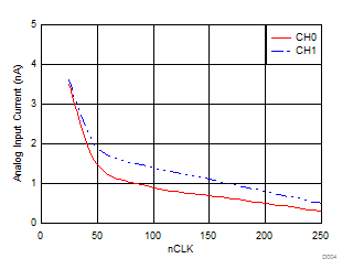
| Input Voltage = 1.5 V | With Low Power Oscillator | |
| Stop Burst Mode | ||
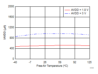
| Stop Burst Mode | With High Speed Oscillator | |
| nCLK = 25 |
6.14 Typical Characteristics for High Precision Mode
At TA = 25°C, AVDD = 3 V, DVDD = 3.3 V, and Two-Channel, Single-Ended Configuration, unless otherwise noted.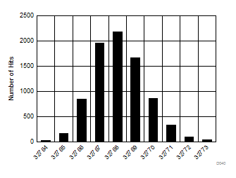
| Standard Deviation = 1.49 | Mean = 32768.5 |
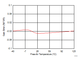
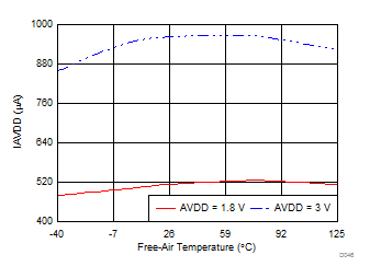
| With High Speed Oscillator | nCLK = 25 | |
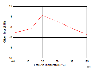
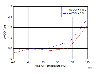
| With Low Power Oscillator | nCLK = 25 | |