SBAS584B October 2013 – August 2014 ADS7253 , ADS7853 , ADS8353
PRODUCTION DATA.
- 1 Features
- 2 Applications
- 3 Description
- 4 Revision History
- 5 Device Comparison Table
- 6 Pin Configurations and Functions
-
7 Specifications
- 7.1 Absolute Maximum Ratings
- 7.2 Handling Ratings
- 7.3 Recommended Operating Conditions
- 7.4 Thermal Information
- 7.5 Electrical Characteristics: ADS8353
- 7.6 Electrical Characteristics: ADS7853
- 7.7 Electrical Characteristics: ADS7253
- 7.8 Electrical Characteristics: All Devices
- 7.9 Timing Requirements: Interface Mode
- 7.10 Timing Characteristics: Serial Interface
- 7.11 Typical Characteristics: ADS8353
- 7.12 Typical Characteristics: ADS7853
- 7.13 Typical Characteristics: ADS7253
- 7.14 Typical Characteristics: Common to ADS8353, ADS7853, and ADS7253
-
8 Detailed Description
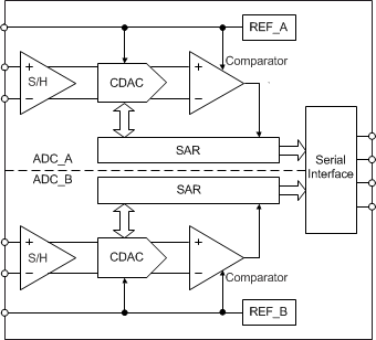
- 8.1 Overview
- 8.2 Functional Block Diagram
- 8.3 Feature Description
- 8.4 Device Functional Modes
- 8.5 Register Maps and Serial Interface
- 9 Application and Implementation
- 10Power-Supply Recommendations
- 11Layout
- 12Device and Documentation Support
- 13Mechanical, Packaging, and Orderable Information
Package Options
Mechanical Data (Package|Pins)
Thermal pad, mechanical data (Package|Pins)
- RTE|16
Orderable Information
8 Detailed Description
8.1 Overview
These devices belong to a family of pin-compatible, dual, high-speed, simultaneous-sampling, analog-to-digital converters (ADCs). The ADS8353, ADS7853, and ADS7253 support single-ended and pseudo-differential input signals. The devices provide a simple, serial interface to the host controller and operate over a wide range of analog and digital power supplies.
These devices have two independently programmable internal references to achieve system-level gain error correction. The Functional Block Diagram section provides a functional block diagram of the device.
8.2 Functional Block Diagram
8.3 Feature Description
8.3.1 Reference
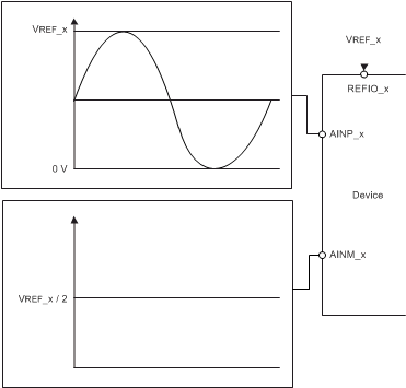
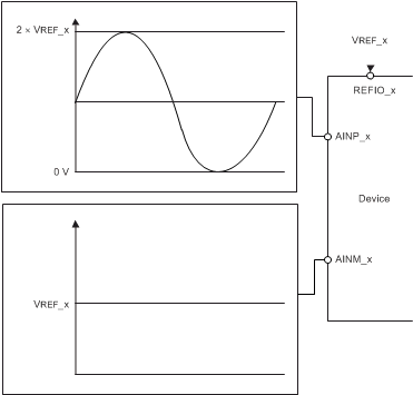
The device has two simultaneous sampling ADCs (ADC_A and ADC_B). ADC_A and ADC_B operate with reference voltages VREF_A and VREF_B present on the REFIO_A and REFIO_B pins, respectively. The REFIO_A and REFIO_B pins should be decoupled with the REFGND_A and REFGND_B pins, respectively, with 10-µF decoupling capacitors.
The device supports operation either with an internal or external reference source, as shown in Figure 84. The reference voltage source is determined by setting bit 6 of the configuration register (CFR.B6). Note that this bit is common to ADC_A and ADC_B.
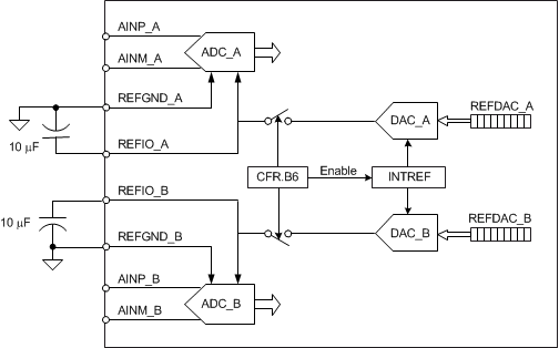 Figure 84. Reference Configurations and Connections
When CFR.B6 is 0, the device shuts down the internal reference source (INTREF) and ADC_A and ADC_B operate on external reference voltages provided by the user on the REFIO_A and REFIO_B pins, respectively.
When CFR.B6 is 1, the device operates with the internal reference source (INTREF) connected to REFIO_A and REFIO_B via DAC_A and DAC_B, respectively. In this configuration, VREF_A and VREF_B can be changed independently by writing to the respective user-programmable registers, REFDAC_A and REFDAC_B, respectively. Refer to the REFDAC Registers (REFDAC_A and REFDAC_B) section for more details.
8.3.2 Analog Inputs
The ADS8353, ADS7853, and ADS7253 support single-ended or pseudo-differential analog inputs on both ADC channels. These inputs are sampled and converted simultaneously by the two ADCs, ADC_A and ADC_B. ADC_A samples and converts (VAINP_A – VAINM_A), and ADC_B samples and converts (VAINP_B – VAINM_B).
Figure 85a and Figure 85b show equivalent circuits for the ADC_A and ADC_B analog input pins, respectively. Series resistance, RS, represents the on-state sampling switch resistance (typically 50 Ω) and CSAMPLE is the device sampling capacitor (typically 40 pF).
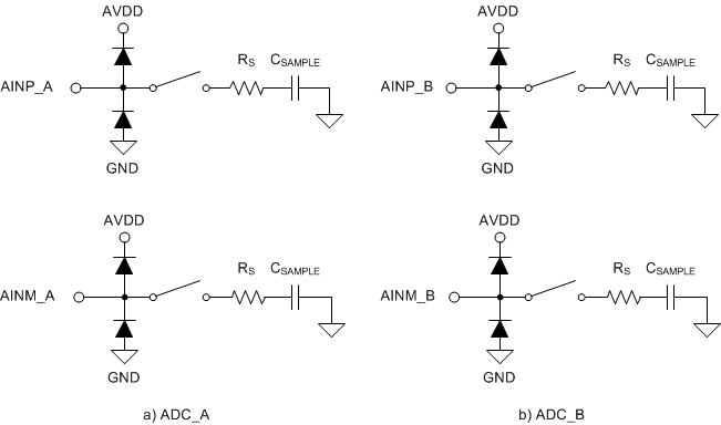 Figure 85. Equivalent Circuit for the Analog Input Pins
8.3.2.1 Analog Input: Full-Scale Range Selection
The full-scale range (FSR) supported at the analog inputs of the device is programmable with bit B9 of the configuration register (CFR.B9). This bit is common for both ADCs (ADC_A and ADC_B). The FSR is given by Equation 1 and Equation 2 :
where
- VREF_A and VREF_B are the reference voltages going to ADC_A and ADC_B, respectively (as described in the Reference section).
Therefore, with appropriate settings of the REFDAC_A and REFDAC_B registers, CFR.B7, and CFR.B9, the maximum dynamic range of the ADC can be used.
Note that while using CFR.B9 set to 1, care must be taken so that the ADC analog supply (AVDD) is as in Equation 3 and Equation 4:
8.3.2.2 Analog Input: Single-Ended and Pseudo-Differential Configurations
The ADS8353, ADS7853, and ADS7253 can support single-ended or pseudo-differential input configurations.
For supporting single-ended inputs, B7 in the configuration register (CFR.B7) must be set to 0 (CFR.B7 = 0) and AINM_A and AINM_B must be externally connected to GND.
For supporting pseudo-differential inputs, CFR.B7 must be set to 1 (CFR.B7 = 1) and AINM_A and AINM_B must be externally connected to FSR_ADC_A / 2 and FSR_ADC_B / 2, respectively. Note that CFR.B7 is common to both ADCs.
The CFR.B9 and CFR.B7 settings can be combined to select the desired input configuration, as shown in Table 1.
Table 1. Input Configurations
| INPUT RANGE SELECTION | AINM SELECTION | CONNECTION DIAGRAM |
|---|---|---|
| CFR.B9 = 0 (FSR_ADC_A = 0 to VREF_A) (FSR_ADC_B = 0 to VREF_B) |
CFR.B7 = 0 (AINM_A = GND) (AINM_B = GND) |
 |
| CFR.B9 = 1 (FSR_ADC_A = 0 to 2 x VREF_A) (FSR_ADC_B = 0 to 2 x VREF_B) |
CFR.B7 = 0 (AINM_A = GND) (AINM_B = GND) |
 |
| CFR.B9 = 0 (FSR_ADC_A = VREF_A) (FSR_ADC_B = VREF_B) |
CFR.B7 = 1 (AINM_A = VREF_A/2) (AINM_B = VREF_B/2) |
 |
| CFR.B9 = 1 (FSR_ADC_A = 2 x VREF_A) (FSR_ADC_B = 2 x VREF_B) |
CFR.B7 = 1 (AINM_A = VREF_A) (AINM_B = VREF_B) |
 |
8.3.3 Transfer Function
The device supports two input configurations:
- Single-ended inputs, CFR.B7 = 0 (default), or
- Pseudo-differential inputs, CFR.B7 = 1.
The device also supports two output data formats:
- Straight binary output, CFR.B4 = 0 (default), or
- Twos compliment output, CFR.B4 = 1.
Device resolution is calculated by Equation 5:
where
- N = 16 (ADS8353), 14 (ADS7853), or 12 (ADS7253) and
- FSR_ADC_x is the full-scale input range of the ADC (refer to the Analog Input section for more details)
Table 2 and Table 3 show the different input voltages and the corresponding output codes from the device.
Table 2. Transfer Characteristics for Straight Binary Output (CFR.B4 = 0, Default)
| INPUT CONFIGURATION | INPUT VOLTAGE | OUTPUT CODE (Hex) | |||||
|---|---|---|---|---|---|---|---|
| STRAIGHT BINARY (CFR.B4 = 0, Default) | |||||||
| AINP_x | AINM_x | AINP_x - AINM_x | CODE | ADS8353 | ADS7853 | ADS7253 | |
| Single-ended (CFR.B7 = 0, default) |
≤ 1 LSB | 0 | ≤ 1 LSB | ZC | 0000 | 0000 | 000 |
| FSR_ADC_x / 2 | FSR_ADC_x / 2 | MC | 7FFF | 1FFF | 7FF | ||
| ≥ FSR_ADC_x – 1 LSB | ≥ FSR_ADC_x – 1 LSB | FSC | FFFF | 3FFF | FFF | ||
| Pseudo-differential (CFR.B7 = 1) |
≤ 1 LSB | FSR_ADC_x / 2 | ≤ –FSR_ADC_x / 2 + 1 LSB | ZC | 0000 | 0000 | 000 |
| FSR_ADC_x / 2 | 0 | MC | 7FFF | 1FFF | 7FF | ||
| ≥ FSR_ADC_x – 1 LSB | ≥ FSR_ADC_x / 2 – 1 LSB | FSC | FFFF | 3FFF | FFF | ||
Table 3. Transfer Characteristics for Twos Compliment Output (CFR.B4 = 1)
| INPUT CONFIGURATION | INPUT VOLTAGE | OUTPUT CODE (Hex) | |||||
|---|---|---|---|---|---|---|---|
| TWOS COMPLIMENT (CFR.B4 = 1) | |||||||
| AINP_x | AINM_x | AINP_x - AINM_x | CODE | ADS8353 | ADS7853 | ADS7253 | |
| Single-ended (CFR.B7 = 0, default) |
≤ 1 LSB | 0 | ≤ 1 LSB | NFSC | 8000 | 2000 | 800 |
| FSR_ADC_x / 2 | FSR_ADC_x / 2 | MC | 0000 | 0000 | 000 | ||
| ≥ FSR_ADC_x – 1 LSB | ≥ FSR_ADC_x – 1 LSB | PFSC | 7FFF | 1FFF | 7FF | ||
| Pseudo-differential (CFR.B7 = 1) |
≤ 1 LSB | FSR_ADC_x / 2 | ≤ –FSR_ADC_x / 2 + 1 LSB | NFSC | 8000 | 2000 | 800 |
| FSR_ADC_x / 2 | 0 | MC | 0000 | 0000 | 000 | ||
| ≥ FSR_ADC_x – 1 LSB | ≥ FSR_ADC_x / 2 – 1 LSB | PFSC | 7FFF | 1FFF | 7FF | ||
Figure 86 shows the ideal device transfer characteristics for the single-ended analog input.
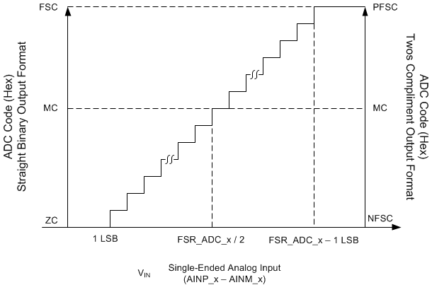 Figure 86. Ideal Transfer Characteristics for a Single-Ended Analog Input
Figure 87 shows the ideal device transfer characteristics for the pseudo-differential analog input.
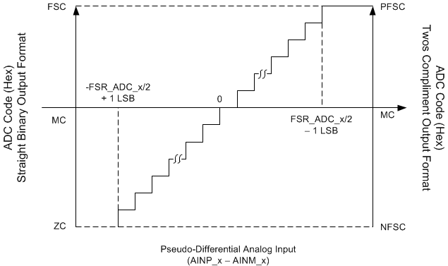 Figure 87. Ideal Transfer Characteristics for a Pseudo-Differential Analog Input
8.4 Device Functional Modes
The device provides three user-programmable registers: the configuration register (CFR), the REFDAC_A register, and the REFDAC_B register. These registers support write (refer to the Write to User Programmable Registers section) and readback (refer to the Reading User-Programmable Registers section) operations and allow the user to customize ADC behavior for specific application requirements.
The device supports four interface modes (refer to the Conversion Data Read section), two low-power modes (refer to the Low-Power Modes section), and short-cycling/reconversion feature (refer to the Frame Abort, Reconversion, or Short-Cycling section).
8.5 Register Maps and Serial Interface
8.5.1 Serial Interface
The device uses the serial clock (SCLK) for synchronizing data transfers in and out of the device.
The CS signal defines one conversion and serial transfer frame. A frame starts with a CS falling edge and ends with a CS rising edge. Between the start and end of the frame, a minimum of N SCLK falling edges must be provided to validate the read or write operation. As shown in Table 4, N depends upon the interface mode used to read the conversion result. When N SCLK falling edges are provided, the write operation attempted in the frame is validated and the internal user-programmable registers are updated on the subsequent CS rising edge. This CS rising edge also ends the frame.
Table 4. SCLK Falling Edges for a Valid Write Operation
| INTERFACE MODE | MINIMUM SCLK FALLING EDGES REQUIRED TO VALIDATE WRITE OPERATION N |
|---|---|
| 32-CLK, dual-SDO mode (default). See the 32-CLK, Dual-SDO Mode section. | 32 |
| 32-CLK, single-SDO mode. See the 32-CLK, Single-SDO Mode section. | 48 |
| 16-CLK, dual-SDO mode. See the 16-CLK, Dual-SDO Mode section. | 16 |
| 16-CLK, single SDO mode. See the 16-CLK, Single SDO Mode section. | 32 |
If CS is brought high before providing N SCLK falling edges, the write operation attempted in the frame is not valid. Refer to the Frame Abort, Reconversion, or Short-Cycling section for more details.
8.5.2 Write to User Programmable Registers
The device features three user-programmable registers: the configuration register (CFR), the REFDAC_A register, and the REFDAC_B register. These registers can be written with the device SDI pin. The first 16 bits of data on SDI are latched into the device on the first 16 SCLK falling edges. However, the new configuration takes effect only when the read or write operation is validated. If these registers are not required to update, SDI must remain low during the respective frames.
The first four SDI data bits (B[15:12]) determine what operation is performed (that is, either a read or write operation or no operation), which register address the operation uses, and the function of the next 12 SDI data bits (B[11:0]). Table 5 lists the various combinations supported for B[15:12].
Table 5. Data Write Operation
| B15 | B14 | B13 | B12 | OPERATION | FUNCTION OF BITS B[11:0] |
|---|---|---|---|---|---|
| 0 | 0 | 0 | 0 | No operation is performed | These bits are ignored |
| 0 | 0 | 0 | 1 | REFDAC_A read | 000h; see the Reading User-Programmable Registers section |
| 0 | 0 | 1 | 0 | REFDAC_B read | 000h; see the Reading User-Programmable Registers section |
| 0 | 0 | 1 | 1 | CFR read | 000h; see the Reading User-Programmable Registers section |
| 1 | 0 | 0 | 0 | CFR write | See the Configuration Register (CFR) section |
| 1 | 0 | 0 | 1 | REFDAC_A write | See the REFDAC_A section |
| 1 | 0 | 1 | 0 | REFDAC_B write | See the REFDAC_B section |
| 1 | 0 | 1 | 1 | No operation is performed | These bits are ignored |
| X | 1 | X | X | No operation is performed | These bits are ignored |
8.5.2.1 Configuration Register (CFR)
The device operation configuration is controlled by the configuration register (CFR) status. Data written into the CFR in a valid frame (F) determine the device configuration for frame (F+1). The bit functions are outlined in Figure 88. On power-up, all bits in the CFR default to 0.
| 15 | 14 | 13 | 12 | 11 | 10 | 9 | 8 |
| WRITE/READ | 0 | ADDR1 | ADDR0 | RD_CLK_ MODE |
RD_DATA_ LINES |
INPUT_RANGE | 0 |
| 7 | 6 | 5 | 4 | 3 | 2 | 1 | 0 |
| INM_SEL | REF_SEL | STANDBY | RD_DATA_ FORMAT |
0 | 0 | 0 | 0 |
Table 6. Configuration Register (CFR) Field Descriptions
| Bit | Field | Type | Reset | Description |
|---|---|---|---|---|
| 15 | WRITE/READ | W | 0h | These bits select the user-programmable register. 1000 = Select this combination to write to the CFR register and to enable bits 11:0 |
| 14 | 0 | R/W | 0h | |
| 13 | ADDR1 | R/W | 0h | |
| 12 | ADDR0 | R/W | 0h | |
| 11 | RD_CLK_MODE | R/W | 0h | This bit provides clock mode selection for the serial interface. 0 = Selects 32-CLK mode (default) 1 = Selects 16-CLK mode (Note that the ADS8353 only supports 32-CLK mode. This bit is ignored for the ADS8353.) |
| 10 | RD_DATA_LINES | R/W | 0h | This bit provides data line selection for the serial interface. 0 = Use SDO_A to output ADC_A data and SDO_B to output of ADC_B data (default) 1 = Use only SDO_A to output of ADC_A data followed by ADC_B data |
| 9 | INPUT_RANGE | R/W | 0h | This bit selects the maximum input range for the ADC as a function of the reference voltage provided to the ADC. See the Analog Inputs section for more details. 0 = FSR equals VREF 1 = FSR equals 2 × VREF |
| 8 | 0 | R/W | 0h | This bit must be set to 0 (default) |
| 7 | INM_SEL | R/W | 0h | This bit selects the voltage to be externally connected to the INM pin. 0 = INM must be externally connected to the GND potential (default) 1 = INM must be externally connected to the FSR_ADC_x / 2 potential |
| 6 | REF_SEL | R/W | 0h | This bit selects the ADC reference voltage source. Refer to the Reference section for more details. 0 = Use external reference (default) 1 = Use internal reference |
| 5 | STANDBY | W | 0h | This bit is used by the device to enter or exit STANDBY mode. Refer to the STANDBY Mode section for more details. |
| 4 | RD_DATA_FORMAT | R/W | 0h | This bit selects the output data format. 0 = Output is in straight binary format (default) 1 = Output is in twos compliment format |
| 3:0 | 0 | R/W | 0h | These bits must be set to 0 (default) |
8.5.2.2 REFDAC Registers (REFDAC_A and REFDAC_B)
The REFDAC registers, bit functions, and resolution information are described in this section.
| 15 | 14 | 13 | 12 | 11 | 10 | 9 | 8 |
| WRITE/READ | 0 | ADDR1 | ADDR0 | D8 | D7 | D6 | D5 |
| 7 | 6 | 5 | 4 | 3 | 2 | 1 | 0 |
| D4 | D3 | D2 | D1 | D0 | 0 | 0 | 0 |
Table 7. REFDAC Registers Field Descriptions
| Bit | Field | Type | Reset | Description |
|---|---|---|---|---|
| 15 | WRITE/READ | W | 0h | These bits select the configurable register address. 1001 = Select this combination to write to the REFDAC_A register 1010 = Select this combination to write to the REFDAC_B register |
| 14 | 0 | R/W | 0h | |
| 13 | ADDR1 | R/W | 0h | |
| 12 | ADDR0 | R/W | 0h | |
| 11:3 | D[8:0] | R/W | 0h | Data to program the individual DAC output voltage. Note: These bits are valid only for bits 15:12 = 1001 or bits 15:12 = 1010. Table 8 shows the relationship between the REFDAC_x programmed value and the DAC_x output voltage. |
| 2:0 | 0 | R/W | 0h | This bit must be set to 0 (default) |
Table 8. REFDAC Settings
| REFDAC_x VALUE (Bits 11:3 in Hex) | B[2:0] | Typical DAC_x OUPTUT VOLTAGE (V)(1) | |||
|---|---|---|---|---|---|
| 1FF (default) | 000 | 2.5000 | |||
| 1FE | 000 | 2.4989 | |||
| 1FD | 000 | 2.4978 | |||
| — | — | — | |||
| 1D7 | 000 | 2.45 | |||
| — | — | — | |||
| 1AE | 000 | 2.40 | |||
| — | — | — | |||
| 186 | 000 | 2.35 | |||
| — | — | — | |||
| 15D | 000 | 2.30 | |||
| — | — | — | |||
| 134 | 000 | 2.25 | |||
| — | — | — | |||
| 10C | 000 | 2.20 | |||
| — | — | — | |||
| 0E3 | 000 | 2.15 | |||
| — | — | — | |||
| 0BA | 000 | 2.10 | |||
| — | — | — | |||
| 091 | 000 | 2.05 | |||
| — | — | — | |||
| 069 | 000 | 2.00 | |||
| — | — | — | |||
| 064 to 000 | 000 | Do not use | |||
8.5.3 Data Read Operation
The device supports two types of read operations: reading user-programmable registers and reading conversion results.
8.5.3.1 Reading User-Programmable Registers
The device supports a readback option for all user-programmable registers: CFR, REFDAC_A, and REFDAC_B. Figure 90 shows a detailed timing diagram for this operation.
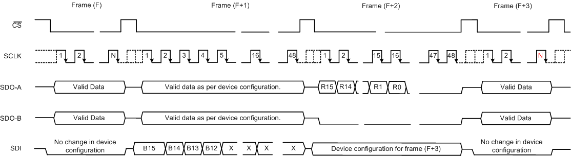
To readback the user-programmable register settings, the appropriate control word should be transmitted to the device during frame (F+1), as shown in Table 9. Frame (F+1) must have at least 48 SCLK falling edges.
Table 9. Control Word to Readback User-Programmable Registers
| USER-PROGRAMMABLE REGISTER | CONTROL WORD TO BE PROGRAMMED IN FRAME (F+1) | |
|---|---|---|
| B[15:12] (Binary) | B[11:0] (Hex) | |
| CFR | 0011b | 000h |
| REFDAC_A | 0001b | 000h |
| REFDAC_B | 0010b | 000h |
Frame (F+2) must have at least 48 SCLK falling edges. During frame (F+2), SDO_A outputs the contents of the selected user-programmable register on the first 16 SCLK falling edges (as shown in Table 10) and then outputs 0s for any subsequent SCLK falling edges. The SDO_B pin outputs 0s for all the SCLK falling edges.
Table 10. Register Data Read Back
| USER-PROGRAMMABLE REGISTER | DATA READ ON SDO-A IN FRAME (F+2) | |||||||||
|---|---|---|---|---|---|---|---|---|---|---|
| R15 | R14 | R13 | R12 | R11 | — | R3 | R2 | R1 | R0 | |
| CFR | 0 | 0 | 1 | 1 | CFG.B11 | — | CFG.B3 | CFG.B2 | CFG.B1 | CFG.B0 |
| REFDAC_A | 0 | 0 | 0 | 1 | REFDAC_A.D8 | — | REFDAC_A.D0 | 0 | 0 | 0 |
| REFDAC_B | 0 | 0 | 1 | 0 | REFDAC_B.D8 | — | REFDAC_B.D0 | 0 | 0 | 0 |
Register settings programmed during frame (F+2) determine the device configuration in frame (F+3).
8.5.3.2 Conversion Data Read
The device provides four different interface modes to the user for reading the conversion result. These modes offer flexible hardware connections and firmware programming. Table 11 shows how to select one of the four interface modes.
Table 11. Interface Mode Selection
| CFR.B11 | CFR.B10 | INTERFACE MODE | MINIMUM SCLK FALLING EDGES REQUIRED TO VALIDATE WRITE OPERATION N |
|---|---|---|---|
| 0 | 0 | 32-CLK, dual-SDO mode (default) | 32 |
| 0 | 1 | 32-CLK, single-SDO mode | 48 |
| 1 | 0 | 16-CLK, dual-SDO mode | 16 |
| 1 | 1 | 16-CLK, single SDO mode | 32 |
In the 32-CLK interface modes, the device uses an internal clock to convert the sampled analog signal. The conversion is completed during the first 16 periods of SCLK and the conversion result can be read on the subsequent SCLK falling edges. All devices in the family (that is, ADS8353, ADS7853, and ADS7253) support the 32-CLK interface modes.
In addition to the 32-CLK interface modes, the ADS7853 and ADS7253 also support the 16-CLK interface modes. By using the 16-CLK interface modes, the same throughput can be achieved at much lower SCLK speeds.
The following sections detail the various interface modes supported by the device.
8.5.3.2.1 32-CLK, Dual-SDO Mode (CFR.B11 = 0, CFR.B10 = 0, Default)
The 32-CLK, dual-SDO mode is the default mode supported by all devices. This mode can also be selected by writing CFR.B11 = 0 and CFR.B10 = 0.
In this mode, the SDO_A pin outputs the ADC_A conversion result and the SDO_B pin outputs the ADC_B conversion result. Figure 91 shows a detailed timing diagram for this mode.
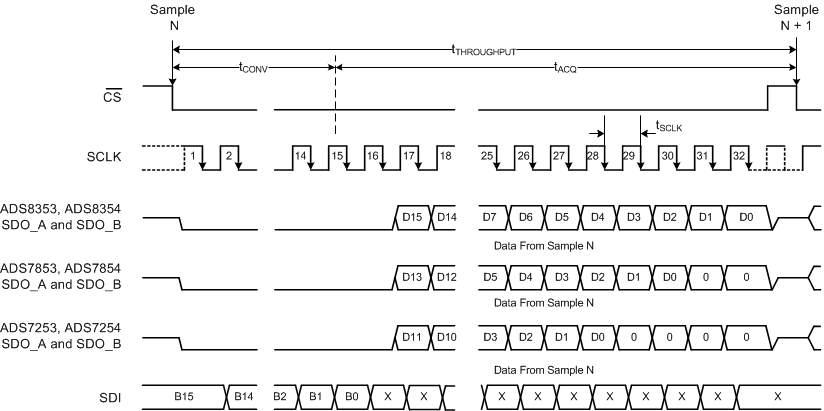 Figure 91. 32-CLK, Dual-SDO Mode Timing Diagram
A CS falling edge brings the serial data bus out of 3-state and also outputs a 0 on the SDO_A and SDO_B pins. The device converts the sampled analog input during the conversion time (tCONV). SDO_A and SDO_B read 0 during this period. After completing the conversion process, the sample-and-hold circuit returns to sample mode. The device outputs the MSBs of ADC_A and ADC_B on SDO_A and SDO_B pins, respectively, on the 16th SCLK falling edge. The subsequent SCLK falling edges are used to shift out the rest of the bits of the conversion result, as shown in Table 12.
Table 12. Data Launch Edge
| DEVICE | PINS | LAUNCH EDGE | ||||||||||||
|---|---|---|---|---|---|---|---|---|---|---|---|---|---|---|
| CS | SCLK | CS | ||||||||||||
| ↓ | ↓1 | — | ↓15 | ↓16 | — | ↓27 | ↓28 | ↓29 | ↓30 | ↓31 | ↓32 ... | ↑ | ||
| ADS8353 | SDO-A | 0 | 0 | — | 0 | D15_A | — | D4_A | D3_A | D2_A | D1_A | D0_A | 0 ... | Hi-Z |
| SDO-B | 0 | 0 | — | 0 | D15_B | — | D4_B | D3_B | D2_B | D1_B | D0_B | 0 ... | Hi-Z | |
| ADS7853 | SDO-A | 0 | 0 | — | 0 | D13_A | — | D2_A | D1_A | D0_A | 0 | 0 | 0 ... | Hi-Z |
| SDO-B | 0 | 0 | — | 0 | D13_B | — | D2_B | D1_B | D0_B | 0 | 0 | 0 ... | Hi-Z | |
| ADS7253 | SDO-A | 0 | 0 | — | 0 | D11_A | — | D0_A | 0 | 0 | 0 | 0 | 0 ... | Hi-Z |
| SDO-B | 0 | 0 | — | 0 | D11_B | — | D0_B | 0 | 0 | 0 | 0 | 0 ... | Hi-Z | |
In this mode, at least 32 SCLK falling edges must be given to validate the read or write frame. A CS rising edge ends the frame and puts the serial bus into 3-state.
Refer to Table 13 for timing specifications specific to this serial interface mode.
Table 13. 32-CLK, Dual-SDO Interface Specific Timing
| PARAMETER | TEST CONDITIONS | MIN | TYP | MAX | UNIT | |
|---|---|---|---|---|---|---|
| TIMING REQUIREMENTS | ||||||
| tCLK | CLOCK period | ADS8353 | 50 | ns | ||
| ADS7853 | 29.4 | ns | ||||
| ADS7253 | 29.4 | ns | ||||
| tACQ | Acquisition time | 33 × tCLK – tCONV | ns | |||
| TIMING SPECIFICATIONS | ||||||
| tCONV | Conversion time | ADS8353 | 730 | ns | ||
| ADS7853 | 450 | ns | ||||
| ADS7253 | 450 | ns | ||||
8.5.3.2.2 32-CLK, Single-SDO Mode (CFR.B11 = 0, CFR.B10 = 1)
The 32-CLK, single-SDO mode provides the option of using only one SDO pin (SDO_A) to read conversion results from both ADCs (ADC_A and ADC_B). SDO_B remains in 3-state and can be treated as a no connect (NC) pin.
This mode can be selected by writing CFR.B11 = 0 and CFR.B10 = 1. Figure 92 shows a detailed timing diagram for this mode.
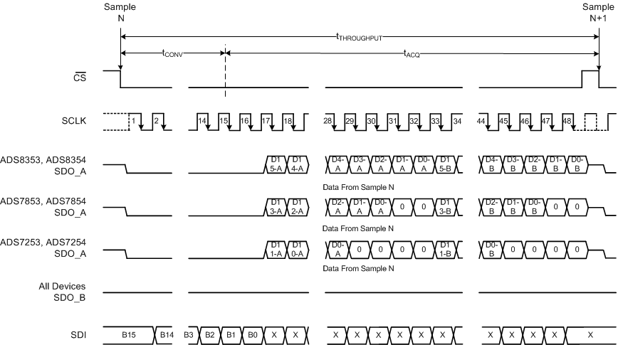 Figure 92. 32-CLK, Single-SDO Mode Timing Diagram
A CS falling edge brings the serial data bus out of 3-state and also outputs a 0 on the SDO_A pin. The device converts the sampled analog input during the conversion time (tCONV). SDO_A reads 0 during this period. After competing the conversion process, the sample-and-hold circuit goes back into sample mode. The device outputs the MSB of ADC_A on the SDO_A pin on the 16th SCLK falling edge. The subsequent SCLK falling edges are used to shift out the conversion result of ADC_A followed by the conversion result of ADC_B on the SDO_A pin, as shown in Table 14.
Table 14. Data Launch Edge
| DEVICE | PIN | LAUNCH EDGE | |||||||||||||||||||
|---|---|---|---|---|---|---|---|---|---|---|---|---|---|---|---|---|---|---|---|---|---|
| CS | SCLK | CS | |||||||||||||||||||
| ↓ | ↓1 | — | ↓15 | ↓16 | — | ↓27 | ↓28 | ↓29 | ↓30 | ↓31 | ↓32 | — | ↓43 | ↓44 | ↓45 | ↓46 | ↓47 | ↓48 ... | ↑ | ||
| ADS8353 | SDO-A | 0 | 0 | — | 0 | D15_A | — | D4_A | D3_A | D2_A | D1_A | D0_A | D15_B | — | D4_B | D3_B | D2_B | D1_B | D0_B | 0 ... | Hi-Z |
| ADS7853 | SDO-A | 0 | 0 | — | 0 | D13_A | — | D2_A | D1_A | D0_A | 0 | 0 | 0 | — | D2_B | D1_B | D0_B | 0 | 0 | 0 ... | Hi-Z |
| ADS7253 | SDO-A | 0 | 0 | — | 0 | D11_A | — | D0_A | 0 | 0 | 0 | 0 | 0 | — | D0_B | 0 | 0 | 0 | 0 | 0 ... | Hi-Z |
In this mode, at least 48 SCLK falling edges must be given to validate the read or write frame. A CS rising edge ends the frame and puts the serial bus into 3-state.
Refer to Table 15 for timing specifications specific to this serial interface mode.
Table 15. 32-CLK, Single-SDO Interface Specific Timing
| PARAMETER | TEST CONDITIONS | MIN | TYP | MAX | UNIT | |
|---|---|---|---|---|---|---|
| TIMING REQUIREMENTS | ||||||
| tCLK | CLOCK period | ADS8353 | 50 | ns | ||
| ADS7853 | 29.4 | ns | ||||
| ADS7253 | 29.4 | ns | ||||
| tACQ | Acquisition time | 49 × tCLK – tCONV | ns | |||
| TIMING SPECIFICATIONS | ||||||
| tCONV | Conversion time | ADS8353 | 730 | ns | ||
| ADS7853 | 450 | ns | ||||
| ADS7253 | 450 | ns | ||||
8.5.3.2.3 16-CLK, Dual-SDO Mode (CFR.B11 = 1, CFR.B10 = 0)
The 16-CLK, dual-SDO mode is designed to support the maximum throughput at lower SCLK frequencies. This interface mode is not supported by the ADS8353.
For the ADS7853 and ADS7253, this interface mode can be selected by writing CFR.B11 = 1 and CFR.B10 = 0. In this mode, the SDO_A pin outputs the ADC_A conversion result and the SDO_B pin outputs the ADC_B conversion result. Figure 93 shows a detailed timing diagram for this mode.
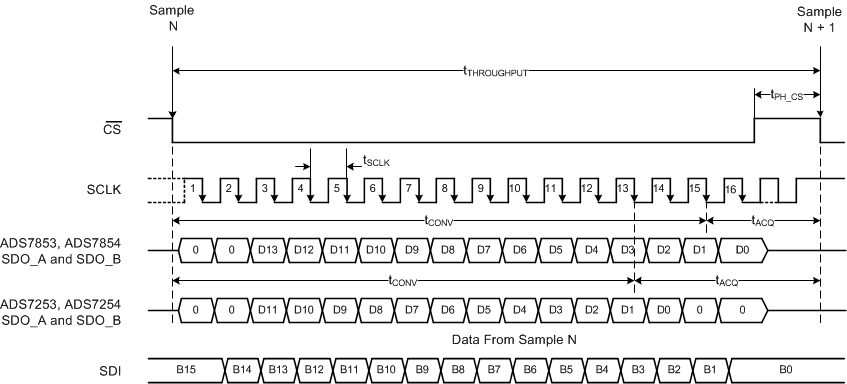 Figure 93. 16-CLK, Dual-SDO Mode Timing Diagram
A CS falling edge brings the serial data bus out of 3-state and also outputs a 0 on the SDO_A and SDO_B pins. The subsequent SCLK falling edges are used for conversion and for data transfer using the serial interface, as shown in Table 16.
The sample-and-hold circuit goes back into sample mode as soon as the conversion process is over.
Table 16. Data Launch Edge
| DEVICE | PINS | LAUNCH EDGE | ||||||||
|---|---|---|---|---|---|---|---|---|---|---|
| CS | SCLK | CS | ||||||||
| ↓ | ↓1 | ↓2 | — | ↓13 | ↓14 | ↓15 | ↓16 ... | ↑ | ||
| ADS7853 | SDO-A | 0 | 0 | D13_A | — | D2_A | D1_A | D0_A | 0 ... | Hi-Z |
| SDO-B | 0 | 0 | D13_B | — | D2_B | D1_B | D0_B | 0 ... | Hi-Z | |
| ADS7253 | SDO-A | 0 | 0 | D11_A | — | D0_A | 0 | 0 | 0 ... | Hi-Z |
| SDO-B | 0 | 0 | D11_B | — | D0_B | 0 | 0 | 0 ... | Hi-Z | |
In this mode, at least 16 SCLK falling edges must be given to validate the read or write frame. A CS rising edge ends the frame and puts the serial bus into 3-state.
Refer to Table 17 for timing specifications specific to this serial interface mode.
Table 17. 16-CLK, Dual-SDO Interface Specific Timing
| PARAMETER | TEST CONDITIONS | MIN | TYP | MAX | UNIT | |
|---|---|---|---|---|---|---|
| TIMING REQUIREMENTS | ||||||
| tCLK | CLOCK period | ADS7853 | 55.5 | ns | ||
| ADS7253 | 55.5 | ns | ||||
| tACQ | Acquisition time | ADS7853 | 4 × tCLK | ns | ||
| ADS7253 | 6 × tCLK | ns | ||||
| TIMING SPECIFICATIONS | ||||||
| tCONV | Conversion time | ADS7853 | 14 × tCLK | ns | ||
| ADS7253 | 12 × tCLK | ns | ||||
8.5.3.2.4 16-CLK, Single-SDO Mode (CFR.B11 = 1, CFR.B10 = 1)
The 16-CLK, single-SDO mode provides the option of using only one SDO pin (SDO_A) and a lower-speed clock to read the conversion results of both ADCs. This interface mode is not supported by the ADS8353.
For the ADS7853 and ADS7253, this mode can be selected by writing CFR.B11 = 1 and CFR.B10 = 1. The SDO_A pin is used to output the conversion results of both ADCs (ADC_A and ADC_B). SDO_B remains in 3-state and can be treated as a no connect (NC) pin. Figure 94 shows a detailed timing diagram for this mode.
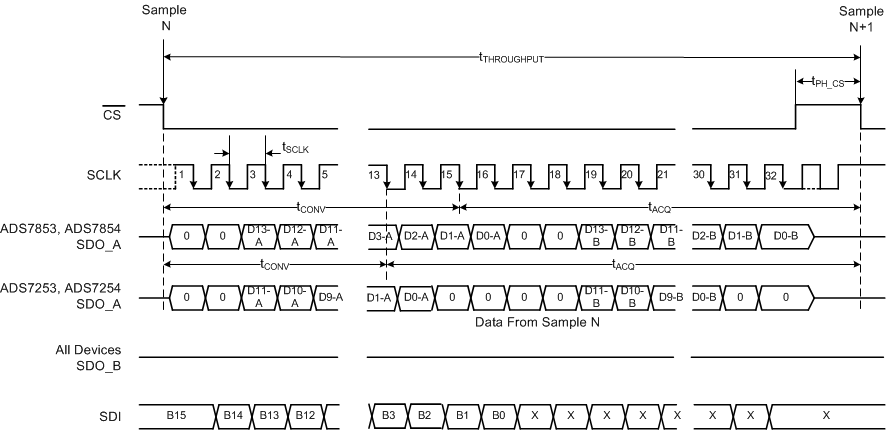 Figure 94. 16-CLK, Single-SDO Mode Timing Diagram
A CS falling edge brings the serial data bus out of 3-state and also outputs a 0 on the SDO_A pin. The subsequent SCLK falling edges are used for conversion and for data transfer using the serial interface, as shown in Table 18.
The sample-and-hold circuit goes back into sample mode as soon as the conversion process is over.
Table 18. Data Launch Edge
| DEVICE | PIN | LAUNCH EDGE | |||||||||||||||
|---|---|---|---|---|---|---|---|---|---|---|---|---|---|---|---|---|---|
| CS | SCLK | CS | |||||||||||||||
| ↓ | ↓1 | ↓2 | — | ↓13 | ↓14 | ↓15 | ↓16 | ↓17 | ↓18 | — | ↓29 | ↓30 | ↓31 | ↓32 ... | ↑ | ||
| ADS7853 | SDO-A | 0 | 0 | D13_A | — | D2_A | D1_A | D0_A | 0 | 0 | D13_B | — | D2_B | D1_B | D0_B | 0 ... | Hi-Z |
| ADS7253 | SDO-A | 0 | 0 | D11_A | — | D0_A | 0 | 0 | 0 | 0 | D11_B | — | D0_B | 0 | 0 | 0 ... | Hi-Z |
In this mode, at least 32 SCLK falling edges must be given to validate the read/write frame. A CS rising edge ends the frame and puts the serial bus into 3-state.
Refer to Table 19 for timing specifications specific to this serial interface mode.
Table 19. 16-CLK, Single-SDO Interface Specific Timing
| PARAMETER | TEST CONDITIONS | MIN | TYP | MAX | UNIT | |
|---|---|---|---|---|---|---|
| TIMING REQUIREMENTS | ||||||
| tCLK | CLOCK period | ADS7853 | 55.5 | ns | ||
| ADS7253 | 55.5 | ns | ||||
| tACQ | Acquisition time | ADS7853 | 19 × tCLK | ns | ||
| ADS7253 | 21 × tCLK | ns | ||||
| TIMING SPECIFICATIONS | ||||||
| tCONV | Conversion time | ADS7853 | 14 × tCLK | ns | ||
| ADS7253 | 12 × tCLK | ns | ||||
8.5.4 Low-Power Modes
In normal mode of operation, all internal circuits of the device are always powered up and the device is always ready to commence a new conversion. This mode enables the device to support the rated throughput. The device also supports two low-power modes to optimize the power consumption at lower throughputs: STANDBY mode and software power-down (SPD) mode.
8.5.4.1 STANDBY Mode
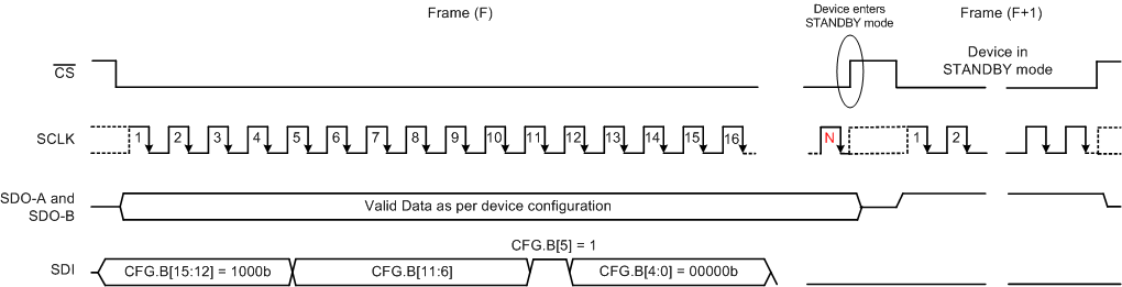
The device supports a STANDBY mode of operation where some of the internal circuits of the device are powered down. However, if bit 6 in configuration register is set to 1 (CFR.B6 = 1), then the internal reference is not powered down and the contents of the REFDAC_A and REFDAC_B registers are retained to enable faster power-up to a normal mode of operation.
As shown in Figure 95, a valid write operation in frame (F) to program the configuration register with B5 set to 1 (CFR.B5 = 1) places the device into a STANDBY mode of operation on the following CS rising edge. While in STANDBY mode, SDO_A and SDO_B output all 1s when CS is low and remain in 3-state when CS is high.
To remain in STANDBY mode, SDI must remain low in the subsequent frames.
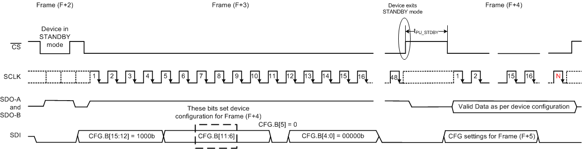
As shown in Figure 96, a valid write operation in frame (F+3) by writing the configuration register with B5 set to 0 (CFR.B5 = 0) brings the device out of STANDBY mode on the following CS rising edge. Frame (F+3) must have at least 48 SCLK falling edges.
After exiting the STANDBY mode, a delay of tPU_STDBY must elapse for the internal circuits to fully power-up and resume normal operation in frame (F+4). Device configuration for frame (F+4) is determined by the status of the CFR.B[11:6] bits programmed during frame (F+3).
Refer to the Timing Characteristics: Serial Interface for timing specifications for this operating mode.
8.5.4.2 Software Power-Down (SPD) Mode
In software power-down (SPD) mode, all internal circuits (including the internal references) are powered down. However, the contents of the REFDAC_A and REFDAC_B registers are retained.
As shown in Figure 97, to enter SPD mode, the device must be selected (by bringing CS low) and SDI must be kept high for a minimum of 48 SCLK cycles during frame (F). The device goes to SPD on the CS rising edge following frame (F). While in SPD mode, SDO_A and SDO_B go to 3-state irrespective of the status of the CS signal.
To remain in SPD mode, SDI must remain high in subsequent frames.
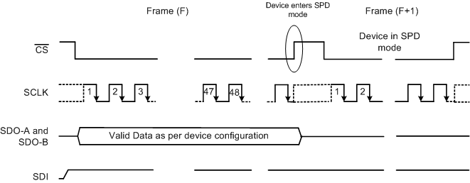 Figure 97. Enter SPD Mode
As shown in Figure 98, to exit SPD mode, the device must be selected (by bringing CS low) and SDI must be kept low for a minimum of 48 SCLK cycles during frame (F+3). The device starts powering-up on a CS rising edge following frame (F+3). After frame (F+3), a delay of tPU_SPD must elapse before programming the configuration register.
A valid write operation in frame (F+4) sets the device configuration for frame (F+5). Frame (F+4) must have at least 48 SCLK falling edges. The output data in frame (F+4) should be discarded.
Refer to the Timing Characteristics: Serial Interface for timing specifications for this operating mode.
8.5.5 Frame Abort, Reconversion, or Short-Cycling
As discussed inFigure 99, the minimum number of SCLK falling edges (N) that must be provided between the beginning and end of the frame depends on the serial interface mode. The SCLK falling edges (N) program the device and retrieve the conversion result. If CS is brought high before the expected number of SCLK falling edges are provided, the current frame is aborted and the device starts sampling the new analog input signal.
If frame (F) is aborted, then the register write operation attempted in frame (F) is considered invalid and the internal registers are not updated. The device continues to have the same configuration in frame (F+1) from frame (F).
The output data bits latched before the CS rising edge are still valid data that correspond to sample N.
 Figure 99. Frame Abort, Reconversion, or Short-Cycling Feature
Refer to the Timing Characteristics: Serial Interface for timing specifications for this operating mode.