SBAS584B October 2013 – August 2014 ADS7253 , ADS7853 , ADS8353
PRODUCTION DATA.
- 1 Features
- 2 Applications
- 3 Description
- 4 Revision History
- 5 Device Comparison Table
- 6 Pin Configurations and Functions
-
7 Specifications
- 7.1 Absolute Maximum Ratings
- 7.2 Handling Ratings
- 7.3 Recommended Operating Conditions
- 7.4 Thermal Information
- 7.5 Electrical Characteristics: ADS8353
- 7.6 Electrical Characteristics: ADS7853
- 7.7 Electrical Characteristics: ADS7253
- 7.8 Electrical Characteristics: All Devices
- 7.9 Timing Requirements: Interface Mode
- 7.10 Timing Characteristics: Serial Interface
- 7.11 Typical Characteristics: ADS8353
- 7.12 Typical Characteristics: ADS7853
- 7.13 Typical Characteristics: ADS7253
- 7.14 Typical Characteristics: Common to ADS8353, ADS7853, and ADS7253
-
8 Detailed Description
- 8.1 Overview
- 8.2 Functional Block Diagram
- 8.3 Feature Description
- 8.4 Device Functional Modes
- 8.5 Register Maps and Serial Interface
- 9 Application and Implementation
- 10Power-Supply Recommendations
- 11Layout
- 12Device and Documentation Support
- 13Mechanical, Packaging, and Orderable Information
Package Options
Mechanical Data (Package|Pins)
Thermal pad, mechanical data (Package|Pins)
- RTE|16
Orderable Information
11 Layout
11.1 Layout Guidelines
Figure 117 shows a board layout example for the ADS8353, ADS7853, and ADS7253 with the WQFN package. Use a ground plane underneath the device and partition the PCB into analog and digital sections. Avoid crossing digital lines with the analog signal path and keep the analog input signals and the reference input signals away from noise sources. As shown in Figure 117, the analog input and reference signals are routed on the left side of the board and the digital connections are routed on the right side of the device.
The power sources to the device must be clean and well-bypassed. Use 10-μF, ceramic bypass capacitors in close proximity to the analog (AVDD) and digital (DVDD) power-supply pins. Avoid placing vias between the AVDD and DVDD pins and the bypass capacitors. Connect all ground pins to the ground plane using short, low impedance paths.
The REFIO-A and REFIO-B reference inputs and outputs are bypassed with 10-μF, X7R-grade, 0805-size, 16-V rated ceramic capacitors (CREF-x). Place the reference bypass capacitors as close as possible to the reference REFIO-x pins and connect the bypass capacitors using short, low-inductance connections. Avoid placing vias between the REFIO-x pins and the bypass capacitors. Small 0.1-Ω to 0.2-Ω resistors (RREF-x) are used in series with the reference bypass capacitors to improve stability.
The fly-wheel RC filters are placed immediately next to the input pins. Among ceramic surface-mount capacitors, COG (NPO) ceramic capacitors provide the best capacitance precision. The type of dielectric used in COG (NPO) ceramic capacitors provides the most stable electrical properties over voltage, frequency, and temperature changes. Figure 117 shows CIN-A and CIN-B filter capacitors placed across the analog input pins of the device.
11.2 Layout Example
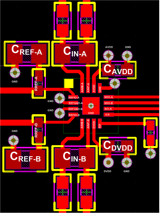 Figure 117. Recommended Layout