SBAS482C January 2010 – September 2017 ADS7924
PRODUCTION DATA.
- 1 Features
- 2 Applications
- 3 Description
- 4 Revision History
- 5 Pin Configuration and Functions
- 6 Specifications
- 7 Detailed Description
-
8 Application and Implementation
- 8.1
Application Information
- 8.1.1 Using an Operational Amplifier Between Multiplexer Output and ADC Input
- 8.1.2 Using an Operational Amplifier and RC Filter Between Multiplexer Output and ADC Input
- 8.1.3 Using an RC Filter Between Multiplexer Output and ADC Input
- 8.1.4 Operational Amplifier With Filter and Gain Option Between Multiplexer Output and ADC Input
- 8.1.5 Driving an RC Filter With an Operational Amplifier Between Multiplexer Output and ADC Input
- 8.1.6 Average Power Consumption
- 8.2 Typical Application
- 8.1
Application Information
- 9 Power Supply Recommendations
- 10Layout
- 11Device and Documentation Support
- 12Mechanical, Packaging, and Orderable Information
Package Options
Mechanical Data (Package|Pins)
- RTE|16
Thermal pad, mechanical data (Package|Pins)
- RTE|16
Orderable Information
7 Detailed Description
7.1 Overview
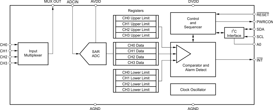
The ADS7924 is a miniature, four-channel, multiplexed, 12-bit, analog-to-digital converter (ADC) with an I2C serial interface. Functional Block Diagram shows a block diagram. The four-channel input multiplexer is routed through external pins to allow a common signal conditioning block to be used for all four channels. The PWRCON digital output can be used to shut down active circuitry used in the signal conditioning; see the Application and Implementation section for additional details.
The successive-approximation-register (SAR) ADC performs a no-latency conversion on the selected input channel and stores the data in a dedicated register. A digital threshold comparator with programmable upper and lower limits can be enabled and used to create an alarm monitor. A dedicated interrupt output pin (INT) indicates when an alarm occurs. Two I2C addresses are available and are selected with the dedicated digital input pin A0. Both standard and fast mode formats for I2C are supported.
7.3 Feature Description
7.3.1 Multiplexer
The ADS7924 has a four-channel, single-ended input multiplexer. As Figure 19 illustrates, ESD diodes protect the inputs. Make sure these diodes do not turn on by staying within the absolute input voltage range specification. The MUXOUT pin can be connected to AGND within the multiplexer (for example, to provide a test signal of 0 V or as part of a calibration procedure). See the PWRCONFIG: Power-Up Configuration Register register in the Register Map section for more details
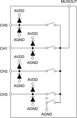 Figure 19. ADS7924 Multiplexer
7.3.2 ADC Input
The ADC Input (ADCIN) pin provides a single-ended input to the 12-bit successive approximation register (SAR) ADC. This pin is protected with ESD diodes in the same way as the multiplexer inputs. While acquiring the signal during the tACQ interval, the ADC sampling capacitor is connected to the ADCIN pin. While converting during the tCONV interval, the sampling capacitor is disconnected from the ADCIN pin, and the conversion process determines the voltage that was sampled.
7.3.3 Reference
The analog supply voltage (AVDD) is used as the reference. Power to the ADS7924 should be clean and well bypassed. A 0.1-μF ceramic capacitor must be placed as close as possible to the ADS7924 package. In addition, a 1-μF to 10-μF capacitor and a 5-Ω to 10-Ω series resistor may be used to low-pass filter a noisy supply.
7.3.4 Clock
The ADS7924 uses an internal clock. The clock speed determines the various timing settings such as conversion time, acquisition time, and so forth.
7.3.5 Data Format
The ADS7924 provides 12 bits of data in unipolar format. The positive full-scale input produces an output code of FFFh and a zero input produces an output code of 0h. The output clips at these codes for signals that either exceed full-scale or go below '0'. Figure 20 illustrates code transitions versus input voltage.

7.3.6 ADC Conversion Timing
The ADS7924 provides a flexible timing arrangement to support a wide variety of measurement needs. Three user-controlled timings include power up (tPU), acquisition (tACQ), and sleep (tSLEEP) plus a fixed conversion time (tCONV).
7.3.6.1 Power-Up Time
The power-up time is allowed to elapse whenever the device has been shutdown in idle mode. Power-up time can allow external circuits, such as an operational amplifier, between the MUXOUT and ADCIN pins to turn on. The nominal time programmed by the PUTIME[4:0] register bits is given by Equation 1:
For example, if PWRUPTIME is set to 25 ('011001') then 50 μs is allowed to elapse before beginning the acquisition time. If a power-up time is not required, set the bits to '0' to effectively bypass.
7.3.6.2 Acquisition Time
The acquisition time is allowed to elapse before beginning a conversion. During this time, the ADC acquires the signal. The minimum acquisition time is 6 µs. The nominal time programmed by the ACQTIME[4:0] register bits is given by Equation 2:
For example, if ACQTIME is set to 30 ('011110') then 66 μs is allowed to acquire the input signal. If an acquisition time greater than 6 μs is not required, set the bits to '0'.
7.3.6.3 Conversion Time
The conversion time is always 4 μs and cannot be programmed by the user.
7.3.6.4 Sleep Time
The sleep time is allowed to elapse after conversions in the Auto-Single with Sleep, Auto-Scan with Sleep, and Auto-Burst Scan with Sleep modes. The nominal time programmed by the SLPTIME registers can be increased by a factor of eight using the SLPMULT8 bit or decreased by a factor of four using the SLPDIV4 bit.
7.3.7 Interrupt Output (INT)
The ADS7924 offers a dedicated output pin (INT) for signaling an interrupt condition. The INT pin can be configured to activate when the ADC is busy with a conversion, when data are ready for retrieval, or when an alarm condition occurs; see the INTCONFIG: Interrupt Configuration Register register in the Register Map section.
To clear an interrupt from an alarm condition, read the INTCONFIG register (12h). To clear an interrupt from data ready, read the data registers. The interrupt clears when the lower four bits are retrieved.
The INT pin can be configured to generate a static output (useful for a host controller monitoring for a level) or a pulse output (useful for a host controller monitoring for a edge transition). When a pulse output is selected, the nominal pulse width is 250 ns. The Interrupt Control Register should be read to clear the interrupt.
7.3.8 PWRCON
The PWRCON pin allows the user to synchronize the shutdown/wakeup of an external operational amplifier with the ADC conversion cycle. This feature provides further power reduction and can be useful in applications where the time difference between consecutive signal captures is large. The PWRCON pin can drive up to 3 mA of current and its output voltage is the same as AVDD. This pin is controlled by the PWRCONFIG register.
7.3.9 Alarm
The ADS7924 offers an independent alarm function for each input channel. An 8-bit window comparator can be enabled to test the ADC conversion result against an upper limit set by the ULR register and against a lower limit set by the LLR register. If the conversion result is less than or equal to the LLR threshold value or greater than or equal to the ULR threshold value, the comparator is tripped. There are separate upper and lower registers for each input channel.
A programmable counter determines how many comparator trips it takes to generate an alarm. A separate counter is used for each channel and is incremented whenever the comparator trips, either for the upper or lower thresholds. That is, an ADC conversion result on channel 1 that exceeds the ULR threshold or falls below the LLR threshold increments the counter for that channel. Figure 21 illustrates a conceptual diagram of the window comparator and alarm circuitry.
When an alarm occurs, the INT pin can be configured to generate an interrupt. The channel that generated the alarm can be read from the registers. A read of the Interrupt Control register clears the alarm register and also resets the alarm counter.
7.4 Device Functional Modes
7.4.1 ADC Operating Modes
The ADS7924 offers multiple operating modes to support a variety of monitoring needs. Conversions can either be started manually or set to automatically continue. The mode is set by writing to the MODE register, and changes take effect as soon as the write completes. Table 1 gives a brief description of each mode.
7.4.1.1 Idle Mode
Use this mode to save power when not converting. All circuits are shut down.
7.4.1.2 Awake Mode
All circuits are operating in this mode and the ADC is ready to convert. When switching between modes, be sure to first select the Awake mode and then switch to the desired mode. This procedure ensures the internal control logic is properly synchronized.

Table 1. Mode Descriptions
| MODE | DESCRIPTION |
|---|---|
| Idle | All circuits shutdown; lowest power setting |
| Awake | All circuits awake and ready to convert |
| Manual-Single | Select input channel is converted once |
| Manual-Scan | All input channels are converted once |
| Auto-Single | One input channel is continuously converted |
| Auto-Scan | All input channels are continuously converted |
| Auto-Single with Sleep | One input channel is continuously converted with programmable sleep time between conversions |
| Auto-Scan with Sleep | All input channels are continuously converted with programmable sleep time between conversions |
| Auto-Burst Scan with Sleep | All input channels are converted with minimal delay followed by a programmable sleep time |
7.4.1.3 Manual-Single Mode
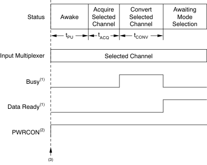
This mode converts the selected channel once; see Figure 22. After the ADC Mode Control register is written, the power-up time (tPU) and acquisition time (tACQ) are allowed to elapse. tPU can be set to '0' to effectively bypass if not needed. tACQ time is programmable through the ACQCONFIG register, bits[4:0]. Sleep time (tSLEEP) is not used in this mode.
After the conversion completes, the device waits for a new mode to be set. This mode can be set to Idle to save power. When tPU and tACQ are very short, the very short conversion time needed allows a read register operation to be issued on the I2C bus immediately after the write operation that initiates this mode.
NOTE
tPU only applies to the first manual-single command.
If multiple conversions are needed, the manual-single mode can be reissued without requiring the awake mode to be issued in between. Consecutive manual-single commands have no tPU period.
7.4.1.4 Manual-Scan Mode
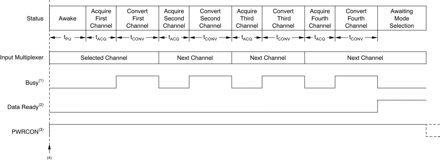
This mode converts all of the channels once, starting with the selected channel, as illustrated in Figure 23. After the ADC Mode Control register is written, the power-up time (tPU) is allowed to elapse. This value can be set to '0' to effectively bypass if not needed. Before each conversion, an acquisition time (tACQ) is allowed to elapse. tACK time is programmable through the ACQCONFIG register, bits[4:0]. Sleep time (tSLEEP) is not used in this mode. The input multiplexer is automatically incremented as the conversions complete. If, for example, the initial selected channel is CH2, the conversion order is CH2, CH3, CH0, and CH1. Data from the conversions are always put into the data register that corresponds to a particular channel. For example, CH2 data always goes in register DATA2_H and DATA2_L regardless of conversion order. After all four conversions complete, the device waits for a new mode to be set. This mode can be set to Idle afterwards to save power. The INT pin can be configured to indicate the completion of each individual conversion or it can wait until all four finish. In either case, the appropriate data register is updated after each conversion. These registers can be read at any time afterwards. If multiple scan are needed, the manual-scan mode can be reissued without requiring the Awake mode to be issued in between.
7.4.1.5 Auto-Single Mode
This mode automatically converts the selected channel continuously; see Figure 24. After the ADC Mode Control register is written, the power-up time (tPU) is allowed to elapse. This value can be set to '0' to effectively bypass if not needed. Before the conversion, an acquisition time (tACQ) is allowed to elapse. tACQ time is programmable through the ACQCONFIG register, bits[4:0]. Sleep time (tSLEEP) is not used in this mode. After the conversion completes the cycle is repeated.
This mode can be used with the onboard digital comparator to monitor the status of an input signal with little support needed from a host microcontroller. The conversion time is less than the I2C data retrieval time. TI suggests stopping this mode by setting the mode to Idle or stopping the conversion by configuring the alarm to do so, before retrieving data. The alarm can also be configured to continue the conversion even after an interrupt is generated.
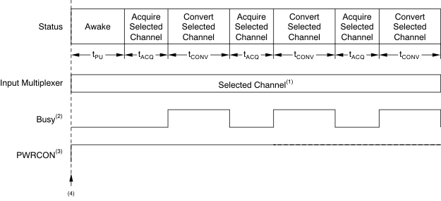
7.4.1.6 Auto-Scan Mode
This mode automatically converts all the channels continuously, starting with the selected channel, as shown in Figure 25. After the ADC Mode Control register is written, the power-up time (tPU) is allowed to elapse. This value can be set to '0' to effectively bypass if not needed. Before the conversion, an acquisition time (tACQ) is allowed to elapse. tACQ time is programmable through the ACQCONFIG register, bits[4:0]. Sleep time (tSLEEP) is not used in this mode. The input multiplexer is automatically incremented as the conversions complete. If, for example, the initial selected channel is CH2, the conversion order is CH2, CH3, CH0, CH1, CH2, CH3, and so forth. until the mode is stopped. Data from the conversions are always put into the data register that corresponds to a particular channel. For example, CH2 data always go in register DATA2_H and DATA2_L regardless of conversion order.
This mode can be used with the onboard digital comparator to monitor the status of the input signals with little support needed from a host microcontroller. TI suggests interrupting this mode and stopping the automatic conversions, either by setting the mode to Idle or configuring the alarm to do so, before retrieving data.

7.4.1.7 Auto-Single With Sleep Mode
This mode automatically converts the selected channel repeatedly with a sleep interval between conversions, as shown in Figure 26. After the ADC Mode Control register is written, the power-up time (tPU) is allowed to elapse. This value can be set to '0' to effectively bypass if not needed. Before the conversion, an acquisition time (tACQ) is allowed to elapse. tACQ time is programmable through the ACQCONFIG register, bits[4:0]. After the conversion, sleep time (tSLEEP) is allowed to elapse and then the cycle repeats. The length of the sleep time is controlled by register bits. During the sleep mode, power dissipation is minimal and the PWRCON output is always disabled.
This mode can be used with the onboard digital comparator to periodically monitor the status of an input signal while saving power between conversions. Little support is needed from a host microcontroller. It is suggested to stop this mode by setting the mode to Idle or stopping the conversion by configuring the alarm to do so, before retrieving data. The length in time of the cycle (tCYCLE) sets the average power dissipation; see Figure 3 or Figure 4.
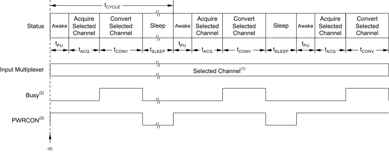
7.4.1.8 Auto-Scan With Sleep Mode
This mode automatically converts all the channels repeatedly with a sleep interval between conversions, as illustrated in Figure 27. After the ADC Mode Control register is written, the power-up time (tPU) is allowed to elapse. This value can be set to '0' to effectively bypass if not needed. Before the first conversion of the selected input, an acquisition time (tACQ) is allowed to elapse. tACQ time is programmable through the ACQCONFIG register, bits[4:0]. After the conversion, a sleep time (tSLEEP) is allowed to elapse and then the cycle repeats. The length of the sleep time is controlled by register bits. During the sleep mode, power dissipation is minimal and the PWRCON output is always disabled. The input multiplexer is automatically incremented as the conversions complete. If, for example, the initial selected channel is CH2, the conversion order is CH2, CH3, CH0, CH1, CH2, CH3, and so forth until the mode is stopped. Data from the conversions are always put into the data register that corresponds to a particular channel. For example, CH2 data always goes in register DATA2_H and DATA2_L regardless of conversion order.
This mode can be used with the onboard digital comparator to periodically monitor the status of the input signals while saving power between conversions. Little support is needed from a host microcontroller. TI suggests stopping this mode by setting it to Idle or stopping the conversion by configuring the alarm to do so, before retrieving data. The length in time of the cycle (tCYCLE) sets the average power dissipation; see Figure 3 or Figure 4.

7.4.1.9 Auto-Burst Scan With Sleep Mode
This mode automatically converts all the channels without delay followed by a sleep interval before the cycle repeats, as illustrated in Figure 28. After the ADC Mode Control register is written, the power-up time (tPU) is allowed to elapse. This value can be set to '0' to effectively bypass if not needed. Before the first conversion of the selected input, an acquisition time (tACQ) is allowed to elapse. tACQ time is programmable through the ACQCONFIG register, bits[4:0]. Afterwards, all four inputs are measured without delay. The input multiplexer is automatically incremented as the conversions complete. If, for example, the initial selected channel is CH2, the conversion order is CH2, CH3, CH0, and CH1. After the four conversions, a sleep time (tSLEEP) is allowed to elapse and then the cycle repeats. The length of the sleep time is controlled by register bits. During the sleep mode, power dissipation is minimal and the PWRCON output is always disabled. Data from the conversions are always put into the data register that corresponds to a particular channel. For example, CH2 data always goes in register DATA2_H and DATA2_L regardless of conversion order.
This mode can be used with the onboard digital comparator to periodically monitor the status of the input signals while saving power between conversions. Little support is needed from a host microcontroller. TI suggests interrupting this mode and stop the automatic conversions, either by setting the mode to Idle or configuring the alarm to do so, before retrieving data. The length in time of the cycle (tCYCLE) sets the average power; see Figure 3 or Figure 4.
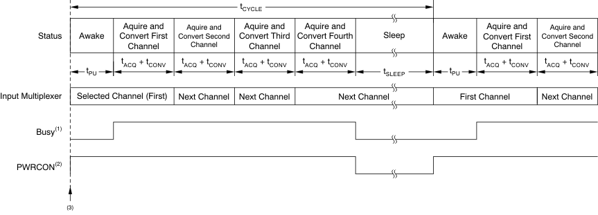
7.5 Programming
7.5.1 I2C Interface
The ADS7924 communicates through an I2C interface. I2C is a two-wire, open-drain interface that supports multiple devices and masters on a single bus. Devices on the I2C bus only drive the bus lines low by connecting them to ground; they never drive the bus lines high. Instead, the bus wires are pulled high by pullup resistors, so the bus wires are high when no device is driving them low. This way, two devices cannot conflict; if two devices drive the bus simultaneously, there is no driver contention.
Communication on the I2C bus always takes place between two devices, one acting as the master and the other as the slave. Both masters and slaves can read and write, but slaves can only do so under the direction of the master. Some I2C devices can act as masters or slaves, but the ADS7924 can only act as a slave device.
An I2C bus consists of two lines, SDA and SCL. SDA carries data; SCL provides the clock. All data are transmitted across the I2C bus in groups of eight bits. To send a bit on the I2C bus, the SDA line is driven to the appropriate level while SCL is low (a low on SDA indicates the bit is zero; a high indicates the bit is one). Once the SDA line settles, the SCL line is brought high, then low. This pulse on SCL clocks the SDA bit into the receiver shift register. If the I2C bus is held idle for more than 25 ms, the bus times out.
The I2C bus is bidirectional: the SDA line is used for both transmitting and receiving data. When the master reads from a slave, the slave drives the data line; when the master sends to a slave, the master drives the data line. The master always drives the clock line. The ADS7924 never drives SCL, because it cannot act as a master. On the ADS7924, SCL is an input only.
Most of the time the bus is idle; no communication occurs, and both lines are high. When communication is taking place, the bus is active. Only master devices can start a communication and initiate a START condition on the bus. Normally, the data line is only allowed to change state while the clock line is low. If the data line changes state while the clock line is high, it is either a START condition or a STOP condition. A START condition occurs when the clock line is high and the data line goes from high to low. A STOP condition occurs when the clock line is high and the data line goes from low to high.
After the master issues a START condition, it sends a byte that indicates which slave device it wants to communicate with. This byte is called the address byte. Each device on an I2C bus has a unique 7-bit address to which it responds. The master sends an address in the address byte, together with a bit that indicates whether it wishes to read from or write to the slave device.
Every byte transmitted on the I2C bus, whether it is address or data, is acknowledged with an acknowledge bit. When the master has finished sending a byte (eight data bits) to a slave, it stops driving SDA and waits for the slave to acknowledge the byte. The slave acknowledges the byte by pulling SDA low. The master then sends a clock pulse to clock the acknowledge bit. Similarly, when the master has finished reading a byte, it pulls SDA low to acknowledge this to the slave. It then sends a clock pulse to clock the bit. (The master always drives the clock line.)
A not-acknowledge is performed by simply leaving SDA high during an acknowledge cycle. If a device is not present on the bus, and the master attempts to address it, it receives a not-acknowledge because no device is present at that address to pull the line low.
When the master has finished communicating with a slave, it may issue a STOP condition. When a STOP condition is issued, the bus becomes idle again. The master may also issue another START condition. When a START condition is issued while the bus is active, it is called a repeated START condition.
See Figure 1 for a timing diagram illustrating the ADS7924 I2C transaction.
7.5.2 I2C Address Selection
The ADS7924 has one address pin, A0, that sets the I2C address. This pin can be connected to ground or VDD, allowing two addresses to be selected with one pin as shown in Table 2. The state of the address pin A0 is sampled continuously.
Table 2. A0 Pin Connection and Corresponding Slave Address
| A0 PIN | SLAVE ADDRESS |
|---|---|
| Ground | 1001000 |
| DVDD | 1001001 |
7.5.3 I2C Speed Modes
The ADS7924 supports the I2C standard and fast modes. Standard mode allows a clock frequency of up to 100 kHz and fast mode permits a clock frequency of up to 400 kHz.
7.5.4 Slave Mode Operations
The ADS7924 can act as either slave receivers or slave transmitters. As a slave device, the ADS7924 cannot drive the SCL line.
7.5.4.1 Receive Mode
In slave receive mode, the first byte transmitted from the master to the slave is the address with the R/W bit low. This byte allows the slave to be written to. The next byte transmitted by the master is the register pointer byte. The ADS7924 then acknowledges receipt of the register pointer byte. The next two bytes are written to the address given by the register pointer. The ADS7924 acknowledges each byte sent. Register bytes are sent with the most significant byte first, followed by the least significant byte.
7.5.4.2 Transmit Mode:
In slave transmit mode, the first byte transmitted by the master is the 7-bit slave address followed by the high R/W bit. This byte places the slave into transmit mode and indicates that the ADS7924 is being read from. The next byte transmitted by the slave is the most significant byte of the register that is indicated by the register pointer. This byte is followed by an acknowledgment from the master. The remaining least significant byte is then sent by the slave and is followed by an acknowledgment from the master. The master may terminate transmission after any byte by not acknowledging or issuing a START or STOP condition.
7.5.5 Writing the Registers
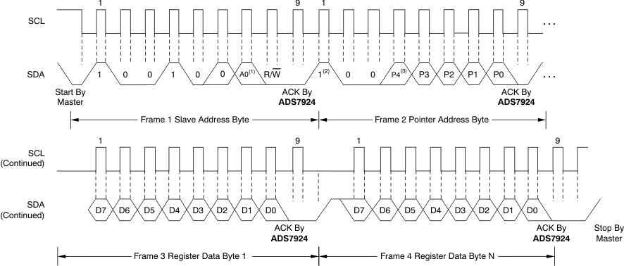
To access a write register from the ADS7924, the master must first write the appropriate value to the Pointer address. The Pointer address is written directly after the slave address byte, low R/W bit, and a successful slave acknowledgment. After the Pointer address is written, the slave acknowledges and the master issues a STOP or a repeated START condition. The MSB of the pointer address is the increment (INC) bit. When set to '1', the register address is automatically incremented after every register write which allows convenient writing of multiple registers. Set INC to '0' when writing a single register. Figure 29 and Figure 30 illustrate timing examples.
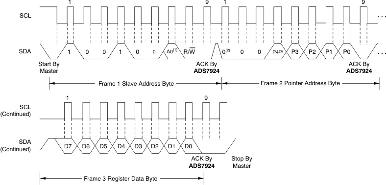
7.5.6 Reading the Registers
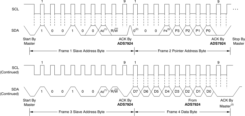
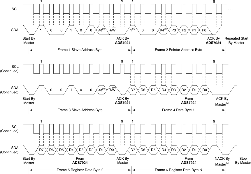
To read a specific register from the ADS7924, the master must first write the appropriate value to the pointer address. The pointer address is written directly after the slave address byte, low R/W bit, and a successful slave acknowledgment. The MSB of the pointer address is the INC bit. When set to '1', the register address is automatically incremented after every register read which allows convenient reading of multiple registers. Set INC to '0' when reading a single register.
The master may issue a START condition and send the slave address byte with the R/W bit high to begin the read. If the previously selected register is to be read again, then updating the pointer address is unnecessary. Figure 31 to Figure 33 provide examples of register reads.

7.6 Register Map
The ADS7924 operation is controlled through a set of registers. Collectively, the registers contain all the information needed to configure the part. Table 3 shows the register map.
Table 3. Register Map
| ADDRESS | REGISTER | RESET VALUE | BIT 7 | BIT 6 | BIT 5 | BIT 4 | BIT 3 | BIT 2 | BIT 1 | BIT 0 |
|---|---|---|---|---|---|---|---|---|---|---|
| 00h | MODECNTRL | 00h | MODE5 | MODE4 | MODE3 | MODE2 | MODE1 | MODE0 | SEL/ID1 | SEL/ID0 |
| 01h | INTCNTRL | X0h | ALRM_ST3 | ALRM_ST2 | ALRM_ST1 | ALRM_ST0 | AEN/ST3 | AEN/ST2 | AEN/ST1 | AEN/ST0 |
| 02h | DATA0_U | XXh | DATA0[11] | DATA0[10] | DATA0[9] | DATA0[8] | DATA0[7] | DATA0[6] | DATA0[5] | DATA0[4] |
| 03h | DATA0_L | XXh | DATA0[3] | DATA0[2] | DATA0[1] | DATA0[0] | 0 | 0 | 0 | 0 |
| 04h | DATA1_U | XXh | DATA1[11] | DATA1[10] | DATA1[9] | DATA1[8] | DATA1[7] | DATA1[6] | DATA1[5] | DATA1[4] |
| 05h | DATA1_L | XXh | DATA1[3] | DATA1[2] | DATA1[1] | DATA1[0] | 0 | 0 | 0 | 0 |
| 06h | DATA2_U | XXh | DATA2[11] | DATA2[10] | DATA2[9] | DATA2[8] | DATA2[7] | DATA2[6] | DATA2[5] | DATA2[4] |
| 07h | DATA2_L | XXh | DATA2[3] | DATA2[2] | DATA2[1] | DATA2[0] | 0 | 0 | 0 | 0 |
| 08h | DATA3_U | XXh | DATA3[11] | DATA3[10] | DATA3[9] | DATA3[8] | DATA3[7] | DATA3[6] | DATA3[5] | DATA3[4] |
| 09h | DATA3_L | XXh | DATA3[3] | DATA3[2] | DATA3[1] | DATA3[0] | 0 | 0 | 0 | 0 |
| 0Ah | ULR0 | XXh | ULR0[7] | ULR0[6] | ULR0[5] | ULR0[4] | ULR0[3] | ULR0[2] | ULR0[1] | ULR0[0] |
| 0Bh | LLR0 | XXh | LLR0[7] | LLR0[6] | LLR0[5] | LLR0[4] | LLR0[3] | LLR0[2] | LLR0[1] | LLR0[0] |
| 0Ch | ULR1 | XXh | ULR1[7] | ULR1[6] | ULR1[5] | ULR1[4] | ULR1[3] | ULR1[2] | ULR1[1] | ULR1[0] |
| 0Dh | LLR1 | XXh | LLR1[7] | LLR1[6] | LLR1[5] | LLR1[4] | LLR1[3] | LLR1[2] | LLR1[1] | LLR1[0] |
| 0Eh | ULR2 | XXh | ULR2[7] | ULR2[6] | ULR2[5] | ULR2[4] | ULR2[3] | ULR2[2] | ULR2[1] | ULR2[0] |
| 0Fh | LLR2 | XXh | LLR2[7] | LLR2[6] | LLR2[5] | LLR2[4] | LLR2[3] | LLR2[2] | LLR2[1] | LLR2[0] |
| 10h | ULR3 | XXh | ULR3[7] | ULR3[6] | ULR3[5] | ULR3[4] | ULR3[3] | ULR3[2] | ULR3[1] | ULR3[0] |
| 11h | LLR3 | XXh | LLR3[7] | LLR3[6] | LLR3[5] | LLR3[4] | LLR3[3] | LLR3[2] | LLR3[1] | LLR3[0] |
| 12h | INTCONFIG | E0h | AIMCNT2 | AIMCNT1 | AIMCNT0 | INTCNFG1 | INTCNFG0 | BUSY/INT | INTPOL | INTTRIG |
| 13h | SLPCONFIG | 00h | 0 | CONVCTRL | SLPDIV4 | SLPMULT8 | 0 | SLPTIME2 | SLPTIME1 | SLPTIME0 |
| 14h | ACQCONFIG | 00h | 0 | 0 | 0 | ACQTIME4 | ACQTIME3 | ACQTIME2 | ACQTIME1 | ACQTIME0 |
| 15h | PWRCONFIG | 00h | CALCNTL | PWRCONPOL | PWRCONEN | PWRUPTIME4 | PWRUPTIME3 | PWRUPTIME2 | PWRUPTIME1 | PWRUPTIME0 |
| 16h | RESET | 18h (A0 = 0) 19h (A0 = 1) |
RST/ID7 | RST/ID6 | RST/ID5 | RST/ID4 | RST/ID3 | RST/ID2 | RST/ID1 | RST/ID0 |
| 7 | 6 | 5 | 4 | 3 | 2 | 1 | 0 |
| MODE5 | MODE4 | MODE3 | MODE2 | MODE1 | MODE0 | SEL/ID1 | SEL/ID0 |
| Bits[7:2] | MODE[5:0]: Mode control |
| 000000 = Idle mode (default) 100000 = Awake mode 110000 = Manual-Single mode 110010 = Manual-Scan mode 110001 = Auto-Single mode 110011 = Auto-Scan mode 111001 = Auto-Single with Sleep mode 111011 = Auto-Scan with Sleep mode 111111 = Auto-Burst Scan with Sleep mode |
|
| Bits[1:0] | SEL/ID[1:0]: Channel selection |
| When read, these bits indicate the last channel converted. When writing to these bits, select which input appears on MUXOUT: 00 = Channel 0 is selected 01 = Channel 1 is selected 10 = Channel 2 is selected 11 = Channel 3 is selected (unless the CALCNTRL bit is set to '1') |
| 7 | 6 | 5 | 4 | 3 | 2 | 1 | 0 |
| ALRM_ST3 | ALRM_ST2 | ALRM_ST1 | ALRM_ST0 | AEN/ST3 | AEN/ST2 | AEN/ST1 | AEN/ST0 |
| Bits[7:4] | ALRM_ST[3:0]: Alarm status (read-only) |
| Reading these bits indicates the alarm status for the channels. These bits are never masked—they always report the alarm status even when the alarm is not enabled by the corresponding AEN/ST bits. Bit 7 = Channel 3 alarm status, '1' indicates an alarm condition Bit 6 = Channel 2 alarm status, '1' indicates an alarm condition Bit 5 = Channel 1 alarm status, '1' indicates an alarm condition Bit 4 = Channel 0 alarm status, '1' indicates an alarm condition |
|
| Bits[3:0] | AEN/ST[3:0]: Alarm enable |
| Writing to these bits enables the alarm for the corresponding channel. Reading these bits returns the status of the alarm for the corresponding channel when enabled. Reading returns a '0' when the alarm in not enabled. Bit 3 = Channel 3 alarm enable, 1 = enabled (default = 0) Bit 2 = Channel 2 alarm enable, 1 = enabled (default = 0) Bit 1 = Channel 1 alarm enable, 1 = enabled (default = 0) Bit 0 = Channel 0 alarm enable, 1 = enabled (default = 0) |
Each input channel has individual registers to buffer the conversion data. The 12 bits are stored in two registers: the upper register stores the eight most significant bits; the lower register stores the lower four least significant bits. The data registers are always updated with the corresponding input channel regardless of the order of conversion. For example, DATA0_U and DATA0_L always contain the results of the latest conversion of CH0.
| 7 | 6 | 5 | 4 | 3 | 2 | 1 | 0 |
| DATA0[11] (MSB) | DATA0[10] | DATA0[9] | DATA0[8] | DATA0[7] | DATA0[6] | DATA0[5] | DATA0[4] |
| 7 | 6 | 5 | 4 | 3 | 2 | 1 | 0 |
| DATA0[3] | DATA0[2] | DATA0[1] | DATA0[0] (LSB) | 0 | 0 | 0 | 0 |
| 7 | 6 | 5 | 4 | 3 | 2 | 1 | 0 |
| DATA1[11] (MSB) | DATA1[10] | DATA1[9] | DATA1[8] | DATA1[7] | DATA1[6] | DATA1[5] | DATA1[4] |
| 7 | 6 | 5 | 4 | 3 | 2 | 1 | 0 |
| DATA1[3] | DATA1[2] | DATA1[1] | DATA1[0] (LSB) | 0 | 0 | 0 | 0 |
| 7 | 6 | 5 | 4 | 3 | 2 | 1 | 0 |
| DATA2[11] (MSB) | DATA2[10] | DATA2[9] | DATA2[8] | DATA2[7] | DATA2[6] | DATA2[5] | DATA2[4] |
| 7 | 6 | 5 | 4 | 3 | 2 | 1 | 0 |
| DATA2[3] | DATA2[2] | DATA2[1] | DATA2[0] (LSB) | 0 | 0 | 0 | 0 |
| 7 | 6 | 5 | 4 | 3 | 2 | 1 | 0 |
| DATA3[11] (MSB) | DATA3[10] | DATA3[9] | DATA3[8] | DATA3[7] | DATA3[6] | DATA3[5] | DATA3[4] |
| 7 | 6 | 5 | 4 | 3 | 2 | 1 | 0 |
| DATA3[3] | DATA3[2] | DATA3[1] | DATA3[0] (LSB) | 0 | 0 | 0 | 0 |
Input channel has individual upper and lower threshold registers. Each register is eight bits with the least significant bit weight equal to AVDD/256. The comparator is tripped when the input signal exceeds the value of the upper limit register or falls below the lower limit register.
| 7 | 6 | 5 | 4 | 3 | 2 | 1 | 0 |
| ULR0[7] (MSB) | ULR0[6] | ULR0[5] | ULR0[4] | ULR0[3] | ULR0[2] | ULR0[1] | ULR0[0] (LSB) |
| 7 | 6 | 5 | 4 | 3 | 2 | 1 | 0 |
| LLR0[7] (MSB) | LLR0[6] | LLR0[5] | LLR0[4] | LLR0[3] | LLR0[2] | LLR0[1] | LLR0[0] (LSB) |
| 7 | 6 | 5 | 4 | 3 | 2 | 1 | 0 |
| ULR1[7] (MSB) | ULR1[6] | ULR1[5] | ULR1[4] | ULR1[3] | ULR1[2] | ULR1[1] | ULR1[0] (LSB) |
| 7 | 6 | 5 | 4 | 3 | 2 | 1 | 0 |
| LLR1[7] (MSB) | LLR1[6] | LLR1[5] | LLR1[4] | LLR1[3] | LLR1[2] | LLR1[1] | LLR0[0] (LSB) |
| 7 | 6 | 5 | 4 | 3 | 2 | 1 | 0 |
| ULR2[7] (MSB) | ULR2[6] | ULR2[5] | ULR2[4] | ULR2[3] | ULR2[2] | ULR2[1] | ULR2[0] (LSB) |
| 7 | 6 | 5 | 4 | 3 | 2 | 1 | 0 |
| LLR2[7] (MSB) | LLR2[6] | LLR2[5] | LLR2[4] | LLR2[3] | LLR2[2] | LLR2[1] | LLR2[0] (LSB) |
| 7 | 6 | 5 | 4 | 3 | 2 | 1 | 0 |
| ULR3[7] (MSB) | ULR3[6] | ULR3[5] | ULR3[4] | ULR3[3] | ULR3[2] | ULR3[1] | ULR3[0] (LSB) |
| 7 | 6 | 5 | 4 | 3 | 2 | 1 | 0 |
| LLR3[7] (MSB) | LLR3[6] | LLR3[5] | LLR3[4] | LLR3[3] | LLR3[2] | LLR3[1] | LLR3[0] (LSB) |
| 7 | 6 | 5 | 4 | 3 | 2 | 1 | 0 |
| ALMCNT2 | ALMCNT1 | ALMCNT0 | INTCNFG2 | INTCNFG1 | INTCNFG0 | INTPOL | INTTRIG |
| Bits[7:5] | ALMCNT[2:0]: Alarm count |
| These bits set the number of times the comparator threshold limit (either upper or lower) must be exceeded to generate an alarm.
000 = Every conversion generates an alarm 001 = Exceeding the threshold limit 1 time generates an alarm condition 010 = Exceeding the threshold limit 2 times generates an alarm condition 011 = Exceeding the threshold limit 3 times generates an alarm condition 100 = Exceeding the threshold limit 4 times generates an alarm condition 101 = Exceeding the threshold limit 5 times generates an alarm condition 110 = Exceeding the threshold limit 6 times generates an alarm condition 111 = Exceeding the threshold limit 7 times generates an alarm condition |
|
| Bits[4:2] | INTCNFG[2:0]: INT output pin configuration |
| These bits determine which signal is output on INT. They also select the conversion control event; see the CONVCTRL bit in the SLPCONFIG register. The configuration of these bits is shown in Table 4. |
Table 4. INT Pin Configuration
| BIT SETTING | INT PIN CONFIGURATION | CONVERSION CONTROL EVENT |
| 000 | Alarm | Alarm |
| 001 | Busy | Alarm |
| 010 | Data ready: one conversion completed | Data ready: one conversion complete |
| 011 | Busy | Data ready: one conversion complete |
| 100 | Do not use | — |
| 101 | Do not use | — |
| 110 | Data ready: all four conversions complete | Data ready: four conversions complete |
| 111 | Busy | Data ready: four conversions complete |
| Bit 1 | INTPOL: INT pin polarity |
| 0 = Active low (default) 1 = Active high |
|
| Bit 0 | INTTRIG: INT output pin signaling |
| 0 = Static signal for use with level triggering (default) 1 = Pulse signal for use with edge triggering |
| 7 | 6 | 5 | 4 | 3 | 2 | 1 | 0 |
| 0 | CONVCTRL | SLPDIV4 | SLPMULT8 | 0 | SLPTIME2 | SLPTIME1 | SLPTIME0 |
| Bit 7 | Always write '0' |
| Bit 6 | CONVCTRL: Conversion control |
| This bit determines the conversion status after a conversion control event; see the INTCNFG bits in the INTCONFIG register. 0 = Conversions continue, independent of the control event status (default) 1 = Conversions are stopped as soon as a control event occurs; the event must be cleared to resume conversions |
|
| Bit 5 | SLPDIV4: Sleep time 4x divider |
| This bit sets the speed of the sleep clock. 0 = Sleep time divider is '1' (default) 1 = Sleep time divider is '4' |
|
| Bit 4 | SLPMULT8: Sleep time 8x multiplier |
| 0 = Sleep time multiplier is '1' (default) 1 = Sleep time multiplier is '8' |
|
| Bit 3 | Always write '0' |
| Bits[2:0] | SLPTIME[2:0]: Sleep time setting |
| 000 = 2.5 ms (default) 001 = 5 ms 010 = 10 ms 011 = 20 ms 100 = 40 ms 101 = 80 ms 110 = 160 ms 111 = 320 ms |
| 7 | 6 | 5 | 4 | 3 | 2 | 1 | 0 |
| 0 | 0 | 0 | ACQTIME4 | ACQTIME3 | ACQTIME2 | ACQTIME1 | ACQTIME0 |
| Bits[7:5] | Always write '0' |
| Bits[4:0] | ACQTIME[4:0]: Signal acquire time |
| These bits set the time to acquire the signal before a conversion (default = 0). tACQ = ACQTIME[4:0] × 2 μs + 6 µs |
| 7 | 6 | 5 | 4 | 3 | 2 | 1 | 0 |
| CALCNTL | PWRCONPOL | PWRCONEN | PWRUPTIME4 | PWRUPTIME3 | PWRUPTIME2 | PWRUPTIME1 | PWRUPTIME0 |
| Bit 7 | CALCNTL: Calibration control |
| 0 = Setting CH3 in the Mode Control register selects the CH3 input to be routed to the MUXOUT pin. (default) 1 = Setting CH3 in the Mode Control register connects the MUXOUT pin to AGND. |
|
| Bit 6 | PWRCONPOL: PWRCON pin polarity |
| 0 = Active low (default) 1 = Active high |
|
| Bit 5 | PWRCONEN: PWRCON enable |
| 0 = The PWRCON pin is disabled (default) 1 = The PWRCON pin is always enabled |
|
| Bits[4:0] | PWRUPTIME[4:0]: Power-up time setting |
| These bits set the power-up time (default = 0). tPWR = PWRUPTIME[4:0] × 2 μs. |
| 7 | 6 | 5 | 4 | 3 | 2 | 1 | 0 |
| RST/ID7 | RST/ID6 | RST/ID5 | RST/ID4 | RST/ID3 | RST/ID2 | RST/ID1 | RST/ID0 |
| A read of this register returns the device ID when A0 determines the last bit of the device ID (0001100A0). A write to this register of 10101010 generates a software reset of the ADS7924. |
