SBAS652A May 2014 – August 2014 ADS7950-Q1 , ADS7951-Q1 , ADS7952-Q1 , ADS7953-Q1 , ADS7954-Q1 , ADS7956-Q1 , ADS7957-Q1 , ADS7958-Q1 , ADS7959-Q1 , ADS7960-Q1 , ADS7961-Q1
PRODUCTION DATA.
- 1 Features
- 2 Applications
- 3 Description
- 4 Revision History
- 5 Device Comparison Table
- 6 Pin Configurations and Functions
-
7 Specifications
- 7.1 Absolute Maximum Ratings
- 7.2 Handling Ratings
- 7.3 Recommended Operating Conditions
- 7.4 Thermal Information
- 7.5 Electrical Characteristics: ADS7950-Q1, ADS7951-Q1, ADS7952-Q1, ADS7953-Q1
- 7.6 Electrical Characteristics: ADS7954-Q1, ADS7956-Q1, ADS7957-Q1
- 7.7 Electrical Characteristics: ADS7958-Q1, ADS7959-Q1, ADS7960-Q1, ADS7961-Q1
- 7.8 Timing Requirements
- 7.9 Typical Characteristics (All ADS79xx-Q1 Family Devices)
- 7.10 Typical Characteristics (12-Bit Devices Only)
- 8 Detailed Description
- 9 Application and Implementation
- 10Power-Supply Recommendations
- 11Layout
- 12Device and Documentation Support
- 13Mechanical, Packaging, and Orderable Information
Package Options
Mechanical Data (Package|Pins)
- DBT|30
Thermal pad, mechanical data (Package|Pins)
Orderable Information
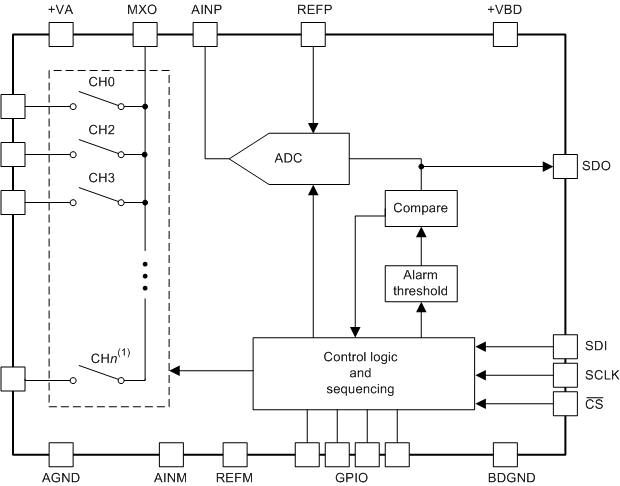
8 Detailed Description
8.1 Overview
The ADS79xx-Q1 device is a high-speed, low-power analog-to-digital converter (ADC) with an 8-bit, 10-bit, and 12-bit multichannel successive-approximation register (SAR). The architecture of the device is based on charge redistribution, which includes a sample and hold function. The ADS79xx-Q1 device uses an external reference and an external serial clock (SCLK) to run the conversion.
The analog input is provided to the CHn input channel. The output of the multiplexer can be shorted directly or can be connected thorough a buffer to the AINP pin. Because the AINM pin is shorted to AGND, when a conversion is initiated, the differential input between the AINP and AGND pins is sampled on the internal capacitor array. Two input ranges are supported. Users can program the input range to either 0 V to Vref or 0 V to 2 × Vref using the mode-control register. The same register can program the input channel sequencing.
The ADS79xx-Q1 device also has four general-purpose input and output (GPIO) pins that can be programmed independently as either general-purpose output (GPO) or general-purpose Input (GPI) pins. GPIOs also support alarm function for which high and low thresholds are programmable per channel.
8.2 Functional Block Diagram
8.3 Feature Description
8.3.1 Device Operation
Figure 45, Figure 46, Figure 47, and Figure 48 illustrate device operation timing. Device operation is controlled with the CS, SCLK, and SDI pins. The device outputs data on the SDO pin.
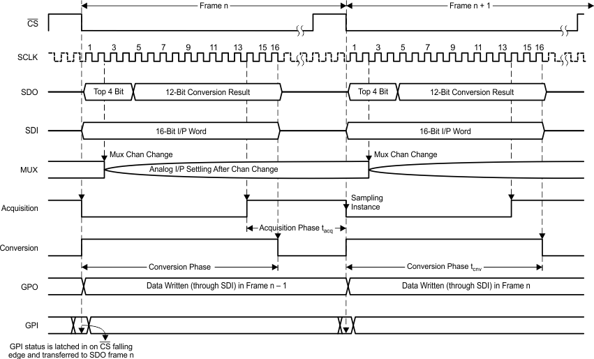 Figure 45. Device Operation Timing Diagram
Each frame begins with the falling edge of the CS pin. With the falling edge of the CS pin, the input signal from the selected channel is sampled, and the conversion process is initiated. The device outputs data while the conversion is in progress. The 16-bit data word contains a 4-bit channel address, followed by a 12-bit conversion result in most-significant-bit (MSB) first format. The GPIO status can be read instead of the channel address (see Table 1, Table 2, and Table 5).
The device selects a new multiplexer channel on the second SCLK falling edge. The acquisition phase begins on the 14th SCLK rising edge. On the next CS falling edge the acquisition phase ends, and the device starts a new frame.
There are four general-purpose IO (GPIO) pins. These pins can be individually programmed as GPO or GPI. Using these pins for preassigned functions is also possible (see Table 11). GPO data can be written into the device through the SDI line. The device refreshes the GPO data on the CS falling edge according to the SDI data written in previous frame.
Similarly the device latches the GPI status on the CS falling edge and outputs the GPI data on the SDO line (if GPI read is enabled by writing DI04 = 1 in the previous frame) in the same frame starting with the CS falling edge.
 Figure 46. Serial Interface Timing Diagram for 8-Bit Devices
 (ADS7958, ADS7959, ADS7960, and ADS7961)
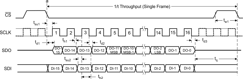 Figure 47. Serial Interface Timing Diagram for 10-Bit Devices (ADS7954, ADS7956, and ADS7957)
 Figure 48. Serial Interface Timing Diagram for 12-Bit Devices
(ADS7950, ADS7951, ADS7952, and ADS7953)
The falling edge of the CS pin clocks out the DO-15 bit (the first bit of the four bit channel address), and remaining address bits are clocked out on every falling edge of SCLK until the third falling edge. The conversion result MSB is clocked out on the fourth SCLK falling edge and LSB on the 11th, 13th, or 15th falling edge respectively for 8-bit, 10-bit, or 12-bit devices. On the 16th falling edge of the SCLK pin, the SDO pin enters tri-state condition. The conversion ends on the 16th falling edge of SCLK.
While the device outputs data on the SDO pin, a 16-bit word is read on the SDI pin. The SDI data are latched on every rising edge of the SCLK pin beginning with the first clock; see Figure 46, Figure 47, and Figure 48.
The CS pin can be asserted (pulled high) only after 16 clocks have elapsed.
The device has two (high and low) programmable alarm thresholds per channel. If the input crosses these limits the device flags out an alarm on the GPIO0 or GPIO1 pin depending on the GPIO-program register settings (see Table 11). The alarm is asserted (under the alarm conditions) on the 12th falling edge of the SCLK pin in the same frame when a data conversion is in progress. The alarm output is reset on the tenth falling edge of the SCLK pin in the next frame.
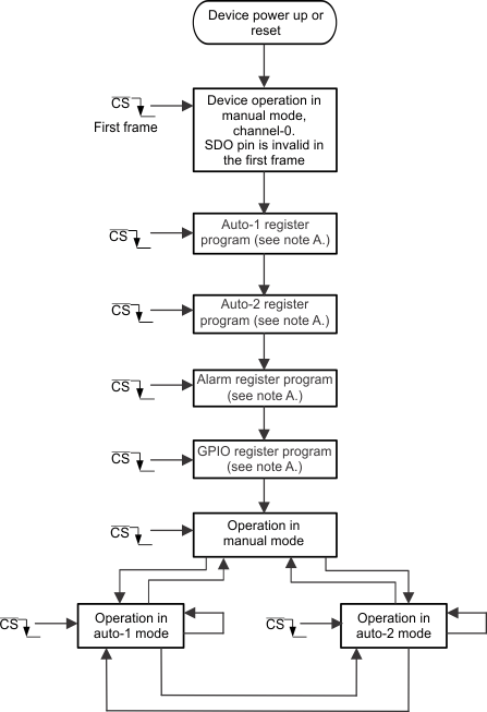
8.3.2 Device Power-up Sequence
Figure 49 illustrates the device power-up sequence. Manual mode is the default power-up channel-sequencing mode and channel-0 is the first channel by default. As explained previously, these devices offer program registers to configure user-programmable features (such as GPIO, alarm, and to preprogram the channel sequence for the auto modes). At power up or on reset, these registers are set to the default values listed in Table 1 to Table 11. Program these registers on power up or after reset. When configured, the device is ready to use in any of the three channel sequencing modes: manual, auto-1, and auto-2.
8.3.3 Analog Input
The ADS79x-Q1 device family offers 8-bit, 10-bit, and 12-bit ADCs with 4-channel, 8-channel, 12-channel, 16-channel multiplexers for analog input. The multiplexer output is available on the MXO pin. The AINP pin is the ADC input pin. The devices offers flexibility for a system designer as both MXO and AINP are accessible externally.
Figure 50 shows the equivalent circuit at the input and output of the multiplexer and the input of the converter during sampling. When the converter enters hold mode, the input impedance at AINP is greater than 1 GΩ.
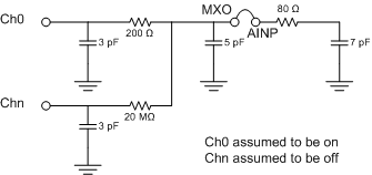 Figure 50. ADC and MUX Equivalent Circuit
When the converter samples an input, the voltage difference between the AINP and AGND pins is captured on the internal capacitor array. The peak input current through the analog inputs depends upon a number of factors including sample rate, input voltage, and source impedance. The current into the ADS79xx-Q1 device charges the internal capacitor array during the sample period. After this capacitance is fully charged, there is no further input current.
To maintain the linearity of the converter, the Ch0 through Chn and AINP inputs must be within the input range limits specified. Outside of these ranges, converter linearity may not meet specifications.
8.3.4 Reference
The ADS79xx-Q1 device can operate with an external 2.5-V ±10-mV reference. A clean, low-noise, well-decoupled reference voltage on the REF pin is required to ensure good performance from the converter. A low-noise, band-gap reference (such as the REF5025 device) can be used to drive this pin. A 10-μF ceramic decoupling capacitor is required between the REF and GND pins of the converter. Place the capacitor as close as possible to the device pins.
8.3.5 Power Saving
The ADS79xx-Q1 device offers a power-down feature to save power when not in use. There are two ways to power down the device. The device can be powered down by writing the DI05 bit equal to 1 in the mode control register (see Table 1, Table 2, and Table 5). In this case, the device powers down on the 16th falling edge of the SCLK pin in the next data frame. Another way to power down the device is through the GPIO pins. The GPIO3 pin can act as a PD input (see Table 11 for assigning this functionality to the GPIO3 pin) which is an asynchronous and active-low input. The device powers down instantaneously after the GPIO3 pin (PD) equals 0. The device powers up again on the CS falling edge when the DI05 bit equals 0 in the mode control register, and the GPIO3 pin (PD) equals 1.
8.4 Device Functional Modes
8.4.1 Channel Sequencing Modes
There are three modes for channel sequencing, including manual mode, auto-1 mode, and auto-2 mode. Mode selection occurs by writing into the control register (see Table 1, Table 2, and Table 5). A new multiplexer channel is selected on the second falling edge of SCLK (as shown in Figure 45) in all three modes.
-
Manual mode: When configured to operate in manual mode, the next selected channel is programmed in each frame and the device selects the programmed channel in the next frame. On power up or after reset the default channel is channel-0 and the device is in manual mode.
-
Auto-1 mode: In this mode the device scans pre-programmed channels in ascending order. A new multiplexer channel is selected every frame on the second falling edge of the SCLK pin. A separate program register preprograms the channel sequence. Table 3 and Table 4 show auto-1 program register settings.
When programmed, the device retains the program register settings until the device is powered down, reset, or reprogrammed. The device is allowed to exit and reenter the auto-1 mode any number of times without disturbing the program register settings.
The auto-1 program register is reset to F, FF, FFF, or FFFF (hex) for the 4-channel, 8-channel, 12-channel, or 16-channel devices, respectively, upon device power up or reset (implying the device scans all channels in ascending order).
-
Auto-2 mode: In this mode the user can configure the program register to select the last channel in the scan sequence. The device scans all channels from channel-0 up to, and including, the last channel in ascending order. The multiplexer channel is selected every frame on the second falling edge of the SCLK pin. A separate program register preprograms the last channel in the sequence (multiplexer depth). Table 6 lists the auto-2 program register settings for selection of the last channel in the sequence.
When programmed, the device retains the program register settings until the device is powered down, reset, or reprogrammed. The device is allowed to exit and re-enter auto-2 mode any number of times, without disturbing the program register settings.
On power up or reset, bits D9 to D6 of the auto-2 program register are reset to 3, 7, B, or F (hex) 4-channel, 8-channel, 12-channel or 16-channel devices, respectively (implying the device scans all channels in ascending order).
8.4.2 Device Programming and Mode Control
The following sections describe device programming and mode control. The ADS79xx-Q1 device feature two types of registers to configure and operate the devices in different modes. These registers are referred as configuration registers. The two types of configuration registers are mode control registers and program registers.
8.4.2.1 Mode Control Register
A mode control register is configured to operate the device in one of three channel sequencing modes, either manual mode, auto-1 mode, or auto-2 mode. This register is also used to control user programmable features, such as range selection, device power-down control, GPIO read control, and writing output data into the GPIO pins.
8.4.2.2 Program Registers
The program registers are used for device-configuration settings and are typically programmed once on power up or after device reset. There are different program registers including auto-1 mode programming for preprogramming the channel sequence, auto-2 mode programming for selection of the last channel in the sequence, alarm programming for all 16 channels (or 4, 8 , or 12 channels depending on the device), and GPIO for individual pin configuration, such as GPI or GPO or a preassigned function.
8.4.3 Operating In Manual Mode
Figure 51 illustrates details regarding entering and running in manual channel-sequencing mode. Table 1 lists the mode control register settings for manual mode in detail. Note that there are no program registers for manual mode.
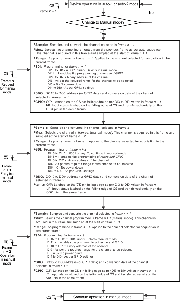 Figure 51. Entering and Running in Manual Channel-Sequencing Mode
Table 1. Mode-Control Register Settings for Manual Mode
| BITS | RESET STATE | DESCRIPTION | ||||
|---|---|---|---|---|---|---|
| LOGIC STATE | FUNCTION | |||||
| DI15-12 | 0001 | 0001 | Selects manual mode | |||
| DI11 | 0 | 1 | Enables programming of bits DI06 through DI00 | |||
| 0 | Device retains values of bits DI06 through DI00 from the previous frame | |||||
| DI10-07 | 0000 | This 4-bit data represents the address of the next channel to be selected in the next frame. DI10 = MSB and DI07 = LSB. For example, 0000 represents channel-0, 0001 represents channel-1, and so on. |
||||
| DI06 | 0 | 0 | Selects 2.5-V input range (range 1) | |||
| 1 | Selects 5-V input range (range 2) | |||||
| DI05 | 0 | 0 | Device normal operation (no power down) | |||
| 1 | Device powers down on 16th SCLK falling edge | |||||
| DI04 | 0 | 0 | The SDO pin outputs the current channel address of the channel on bits DO15 through DO12 followed by a 12-bit conversion result on bits DO11 through DI00. | |||
| 1 | The GPIO3 through GPIO0 data (both input and output) is mapped onto bits DO15 through DO12 in the order shown below. Lower data bits DO11 through DO00 represent the 12-bit conversion result of the current channel. | |||||
| DOI5 | DOI4 | DOI3 | DOI2 | |||
| GPIO3 | GPIO2 | GPIO1 | GPIO0 | |||
| DI03-00 | 0000 | The GPIO data for the channels configured as an output. The device ignores the data for the channel which is configured as input. The SDI bit and corresponding GPIO information is given below. | ||||
| DI03 | DI02 | DI01 | DI00 | |||
| GPIO3 | GPIO2 | GPIO1 | GPIO0 | |||
8.4.4 Operating In Auto-1 Mode
Figure 52 shows a flowchart containing the details regarding entering and running in auto-1 channel-sequencing mode. Table 2 lists the mode control register settings for auto-1 mode in detail.
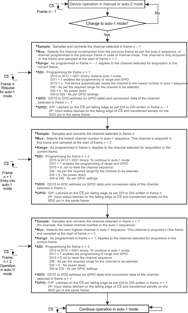 Figure 52. Entering and Running in Auto-1 Channel-Sequencing Mode
Table 2. Mode-Control Register Settings for Auto-1 Mode
| BITS | RESET STATE | DESCRIPTION | ||||
|---|---|---|---|---|---|---|
| LOGIC STATE | FUNCTION | |||||
| DI15-12 | 0001 | 0010 | Selects auto-1 mode | |||
| DI11 | 0 | 1 | Enables programming of bits DI10 through DI00 | |||
| 0 | Device retains values of bits DI10 through DI00 from previous frame | |||||
| DI10 | 0 | 1 | The channel counter is reset to the lowest programmed channel in the auto-1 program register | |||
| 0 | The channel counter increments every conversion (no reset) | |||||
| DI09-07 | 000 | xxx | Do not care | |||
| DI06 | 0 | 0 | Selects 2.5-V input range (range 1) | |||
| 1 | Selects 5-V input range (range 2) | |||||
| DI05 | 0 | 0 | Device normal operation (no powerdown) | |||
| 1 | Device powers down on the 16th SCLK falling edge | |||||
| DI04 | 0 | 0 | SDO outputs current channel address of the channel on DO15..12 followed by 12-bit conversion result on DO11 through DO00. | |||
| 1 | The GPIO3 to GPIO0 data (both input and output) is mapped onto DO15 through DO12 in the order shown below. Lower data bits DO11 through DO00 represent the 12-bit conversion result of the current channel. | |||||
| DO15 | DO14 | DO13 | DO12 | |||
| GPIO3 | GPIO2 | GPIO1 | GPIO0 | |||
| DI03-00 | 0000 | The GPIO data for the channels configured as an output. The device ignores the data for the channel which is configured as input. The SDI bit and corresponding GPIO information is given below | ||||
| DI03 | DI02 | DI01 | DI00 | |||
| GPIO3 | GPIO2 | GPIO1 | GPIO0 | |||
The auto-1 program register is programmed (once on power up or reset) to preselect the channels for the auto-1 sequence, as shown in Figure 53. The auto-1 program-register programming requires two CS frames for complete programming. In the first CS frame, the device enters the auto-1 register programming sequence, and in the second frame the device programs the auto-1 program register. For complete details see Table 2, Table 3, and Table 4.
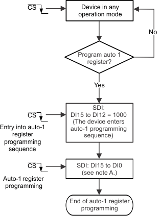
Table 3. Program Register Settings for Auto-1 Mode
| BITS | RESET STATE | DESCRIPTION | |
|---|---|---|---|
| LOGIC STATE | FUNCTION | ||
| FRAME 1 | |||
| DI15-12 | NA | 1000 | The device enters auto-1 program sequence. Device programming occurs in the next frame. |
| DI11-00 | NA | Do not care | |
| FRAME 2 | |||
| DI15-00 | All 1's | 1 (individual bit) | A particular channel is programmed to be selected in the channel scanning sequence. The channel numbers are mapped one-to-one with respect to the SDI bits. For example, DI15 → Ch15, DI14 → Ch14 … DI00 → Ch00 |
| 0 (individual bit) | A particular channel is programmed to be skipped in the channel scanning sequence. The channel numbers are mapped one-to-one with respect to the SDI bits. For example, DI15 → Ch15, DI14 → Ch14 … DI00 → Ch00 |
||
Table 4. Mapping of Channels to SDI Bits
| DEVICE(1) | SDI BITS | |||||||||||||||
|---|---|---|---|---|---|---|---|---|---|---|---|---|---|---|---|---|
| DI15 | DI14 | DI13 | DI12 | DI11 | DI10 | DI09 | DI08 | DI07 | DI06 | DI05 | DI04 | DI03 | DI02 | DI01 | DI00 | |
| 4 Channel | X | X | X | X | X | X | X | X | X | X | X | X | 1/0 | 1/0 | 1/0 | 1/0 |
| 8 Channel | X | X | X | X | X | X | X | X | 1/0 | 1/0 | 1/0 | 1/0 | 1/0 | 1/0 | 1/0 | 1/0 |
| 12 Channel | X | X | X | X | 1/0 | 1/0 | 1/0 | 1/0 | 1/0 | 1/0 | 1/0 | 1/0 | 1/0 | 1/0 | 1/0 | 1/0 |
| 16 Channel | 1/0 | 1/0 | 1/0 | 1/0 | 1/0 | 1/0 | 1/0 | 1/0 | 1/0 | 1/0 | 1/0 | 1/0 | 1/0 | 1/0 | 1/0 | 1/0 |
8.4.5 Operating In Auto-2 Mode
Figure 54 illustrates the details regarding entering and running in auto-2 channel-sequencing mode. Table 5 lists the mode-control register settings for auto-2 mode in detail.
Table 5. Mode-Control Register Settings for Auto-2 Mode
| BITS | RESET STATE | DESCRIPTION | ||||
|---|---|---|---|---|---|---|
| LOGIC STATE | FUNCTION | |||||
| DI15-12 | 0001 | 0011 | Selects auto-2 mode | |||
| DI11 | 0 | 1 | Enables programming of bits DI10 through DI00 | |||
| 0 | The device retains values of DI10 through DI00 from the previous frame | |||||
| DI10 | 0 | 1 | The channel number is reset to Ch-00 | |||
| 0 | The channel counter increments every conversion (no reset) | |||||
| DI09-07 | 000 | xxx | Do not care | |||
| DI06 | 0 | 0 | Selects 2.5-V input range (range 1) | |||
| 1 | Selects 5-V input range (range 2) | |||||
| DI05 | 0 | 0 | Device normal operation (no powerdown) | |||
| 1 | The device powers down on the 16th SCLK falling edge | |||||
| DI04 | 0 | 0 | The SDO pin outputs the current channel address of the channel on bits DO15 through DO12 followed by the 12-bit conversion result on bits DO11 through DO00. | |||
| 1 | The GPIO3 to GPIO0 data (both input and output) is mapped onto bits DO15 through DO12 in the order shown below. Lower data bits DO11 through DO00 represent the 12-bit conversion result of the current channel. | |||||
| DO15 | DO14 | DO13 | DO12 | |||
| GPIO3 | GPIO2 | GPIO1 | GPIO0 | |||
| DI03-00 | 0000 | The GPIO data for the channels configured as an output. The device ignores data for the channel that is configured as input. The SDI bit and corresponding GPIO information is given below. | ||||
| DI03 | DI02 | DI01 | DI00 | |||
| GPIO3 | GPIO2 | GPIO1 | GPIO0 | |||
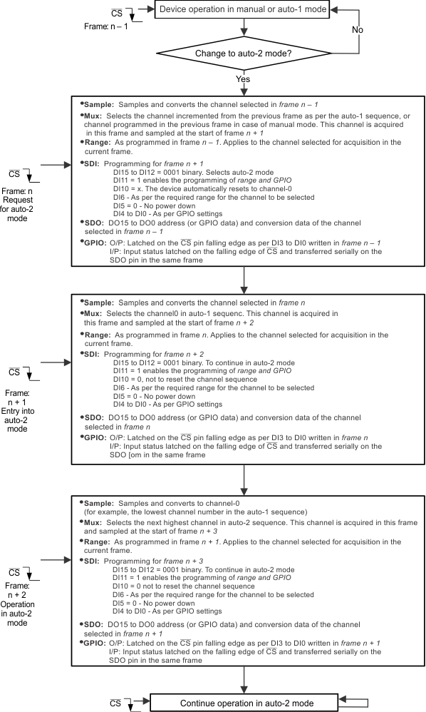 Figure 54. Entering and Running in Auto-2 Channel-Sequencing Mode
The auto-2 program register is programmed (once on power up or reset) to preselect the last channel (or sequence depth) in the auto-2 sequence. Unlike auto-1 program-register programming, auto-2 program-register programming requires only one CS frame for complete programming. Figure 55 and Table 6 provide complete details.
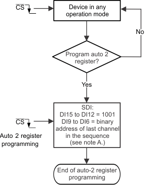
Table 6. Program Register Settings for Auto-2 Mode
| BITS | RESET STATE | DESCRIPTION | |
|---|---|---|---|
| LOGIC STATE | FUNCTION | ||
| DI15-12 | NA | 1001 | The auto-2 program register is selected for programming |
| DI11-10 | NA | Do not care | |
| DI09-06 | NA | aaaa | This 4-bit data represents the address of the last channel in the scanning sequence. During device operation in auto-2 mode, the channel counter begins at CH-00 and increments every frame until the counter equals aaaa. The channel counter then rolls over to CH-00 in the next frame. |
| DI05-00 | NA | Do not care | |
8.4.6 Continued Operation In A Selected Mode
When a device is programmed to operate in one of the modes, the user can continue to operate in the same mode. Table 7 lists mode-control register settings to continue operating in a selected mode.
Table 7. Continued Operation in a Selected Mode
| BITS | RESET STATE | DESCRIPTION | |
|---|---|---|---|
| LOGIC STATE | FUNCTION | ||
| DI15-12 | 0001 | 0000 | The device continues to operate in the selected mode. In auto-1 and auto-2 modes the channel counter increments normally, whereas in the manual mode the device continues with the last selected channel. The device ignores data on bits DI11-DI00 and continues operating as per the previous settings. This feature is provided so that the SDI pin can be held low when no changes are required in the mode-control register settings. |
| DI11-00 | All 0 | The device ignores these bits when bit DI15-12 is set to 0000 logic state | |
8.5 Digital Output Code
As discussed previously in the Device Operation section, the digital output of the ADS79xx-Q1 devices is SPI™ compatible. Table 8, Table 9, and Table 10 list the output codes corresponding to various analog input voltages.
Table 8. Ideal Input Voltages and Output Codes for 8-Bit Devices
(ADS7958, ADS7959, ADS7960, and ADS7961)
| DESCRIPTION | ANALOG VALUE | DIGITAL OUTPUT STRAIGHT BINARY |
||
|---|---|---|---|---|
| BINARY CODE | HEX CODE | |||
| Full-scale range | Range 1 → Vref | Range 2 → 2 × Vref | — | — |
| Least-significant bit (LSB) | Vref / 256 | 2 × Vref / 256 | — | — |
| Full scale | Vref – 1 LSB | 2 × Vref – 1 LSB | 1111 1111 | FF |
| Midscale | Vref / 2 | Vref | 1000 0000 | 80 |
| Midscale – 1 LSB | Vref / 2 – 1 LSB | Vref – 1 LSB | 0111 1111 | 7F |
| Zero | 0 V | 0 V | 0000 0000 | 00 |
Table 9. Ideal Input Voltages and Output Codes for 10-Bit Devices
(ADS7958, ADS7959, ADS7960, and ADS7961)
| DESCRIPTION | ANALOG VALUE | DIGITAL OUTPUT STRAIGHT BINARY |
||
|---|---|---|---|---|
| BINARY CODE | HEX CODE | |||
| Full-scale range | Range 1 → Vref | Range 2 → 2 × Vref | — | — |
| Least-significant bit (LSB) | Vref / 1024 | 2 × Vref / 1024 | — | — |
| Full scale | Vref – 1 LSB | 2 Vref – 1 LSB | 11 1111 1111 | 3FF |
| Midscale | Vref / 2 | Vref | 10 0000 0000 | 200 |
| Midscale – 1 LSB | Vref / 2 – 1 LSB | Vref – 1 LSB | 01 1111 1111 | 1FF |
| Zero | 0 V | 0 V | 00 0000 0000 | 000 |
Table 10. Ideal Input Voltages and Output Codes for 12-Bit Devices
(ADS7950, ADS7951, ADS7952, and ADS7953)
| DESCRIPTION | ANALOG VALUE | DIGITAL OUTPUT STRAIGHT BINARY |
||
|---|---|---|---|---|
| BINARY CODE | HEX CODE | |||
| Full-scale range | Range 1 → Vref | Range 2 → 2 × Vref | — | — |
| Least-significant bit (LSB) | Vref / 4096 | 2 × Vref / 4096 | — | — |
| Full scale | Vref – 1 LSB | 2 × Vref – 1 LSB | 1111 1111 1111 | FFF |
| Midscale | Vref / 2 | Vref | 1000 0000 0000 | 800 |
| Midscale – 1 LSB | Vref / 2 – 1 LSB | Vref – 1 LSB | 0111 1111 1111 | 7FF |
| Zero | 0 V | 0 V | 0000 0000 0000 | 000 |
8.6 Programming: GPIO
8.6.1 GPIO Registers
The device has four general-purpose input and output (GPIO) pins. Each of the four pins can be independently programmed as general purpose output (GPO) or general purpose input (GPI). Using the GPIOs pins for some preassigned functions (see Table 11) is possible. The GPO data can be written into the device through the SDI line. The device refreshes the GPO data on every CS falling edge as per the SDI data written in the previous frame. Similarly, the device latches the GPI status on the CS falling edge and outputs it on the SDO pin (if the GPI pin is read-enabled by writing bit DI04 equal to 1 during the previous frame) in the same frame starting on the CS falling edge.
Figure 56 shows the details regarding programming the GPIO registers. Table 11 lists the details regarding GPIO-register programming settings.
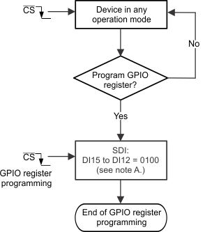
Table 11. GPIO Program-Register Settings
| BITS | RESET STATE | DESCRIPTION | |
|---|---|---|---|
| LOGIC STATE | FUNCTION | ||
| DI15-12 | NA | 0100 | The device selects GPIO program registers for programming. |
| DI11-10 | 00 | 00 | Do not program these bits to any logic state other than 00. |
| DI09 | 0 | 1 | The device resets all registers in the next CS frame to the reset state shown in the corresponding tables (the device also resets itself). |
| 0 | Device normal operation. | ||
| DI08 | 0 | 1 | The device configures the GPIO3 pin as the device power-down input. |
| 0 | The GPIO3 pin remains a general-purpose input or output. | ||
| DI07 | 0 | 1 | The device configures the GPIO2 pin as a device-range input. |
| 0 | The GPIO2 pin remains a general-purpose input or output. | ||
| DI06-04 | 000 | 000 | The GPIO1 and GPIO0 pins remain a general-purpose input or output. |
| xx1 | The device configures the GPIO0 pin as a high-alarm or low-alarm output. This output is active high. GPIO1 remains general-purpose input or output. | ||
| 010 | The device configures GPIO0 as a high-alarm output. This output is active high. The GPIO1 pin remains a general-purpose input or output. | ||
| 100 | The device configures GPIO1 as a low-alarm output. This output is active high. The GPIO0 pin remains a general-purpose input or output. | ||
| 110 | The device configures GPIO1 as a low-alarm output and the GPIO0 pin as a high-alarm output. These outputs are active high. | ||
| Note: The following settings are valid for the GPIO pins that are not assigned a specific function through bits DI08 to DI04 | |||
| DI03 | 0 | 1 | The GPIO3 pin is configured as general-purpose output. |
| 0 | The GPIO3 pin is configured as general-purpose input. | ||
| DI02 | 0 | 1 | The GPIO2 pin is configured as general-purpose output. |
| 0 | The GPIO2 pin is configured as general-purpose input. | ||
| DI01 | 0 | 1 | The GPIO1 pin is configured as general-purpose output. |
| 0 | The GPIO1 pin is configured as general-purpose input. | ||
| DI00 | 0 | 1 | The GPIO0 pin is configured as general-purpose output. |
| 0 | The GPIO0 pin is configured as general-purpose input. | ||
8.6.2 Alarm Thresholds for GPIO Pins
Each channel has two alarm program registers, one for setting the high alarm threshold and the other for setting the low alarm threshold. For ease of programming, two alarm programming registers per channel, corresponding to four consecutive channels, are assembled into one group (a total of eight registers). There are four of these groups for 16-channel devices, and one, two or three of these groups for the 12-, 8-, or 4-channel devices, respectively. Table 12 lists the grouping of the various channels for each device in the ADS79xx-Q1 family. Figure 57 illustrates the details regarding programming the alarm thresholds. Table 13 lists the details regarding the alarm-program register settings.
Table 12. Grouping of Alarm Program Registers
| GROUP NUMBER | REGISTERS | APPLICABLE FOR DEVICE |
|---|---|---|
| 0 | High and low alarm for channel 0, 1, 2, and 3 | ADS750, ADS7952, ADS7951, and ADS7953; ADS7954, ADS7956, and ADS7957; ADS7958, ADS7959, ADS7960, and ADS7961 |
| 1 | High and low alarm for channel 4, 5, 6, and 7 | ADS7951, ADS7952, and ADS7953; ADS7956, and ADS7957; ADS7959, ADS7960, and ADS7961 |
| 2 | High and low alarm for channel 8, 9, 10, and 11 | ADS7953 and ADS7952, ADS7957 and ADS7956, ADS7961 and ADS7960 |
| 3 | High and low alarm for channel 12, 13, 14, and 15 | ADS7953, ADS7957, and ADS7961 |
Each alarm group requires nine CS frames for programming the respective alarm thresholds. In the first frame the device enters the programming sequence and in each subsequent frame the device programs one of the registers from the group. The device offers a feature to program less than eight registers in one programming sequence. The device exits the alarm threshold programming sequence in the next frame after encountering the first exit alarm program bit high.
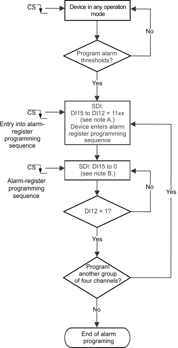
Table 13. Alarm Program Register Settings
| BITS | RESET STATE | DESCRIPTION | |
|---|---|---|---|
| LOGIC STATE | FUNCTION | ||
| FRAME 1 | |||
| DI15-12 | NA | 1100 | The device enters alarm programming sequence for group 0 |
| 1101 | The device enters alarm programming sequence for group 1 | ||
| 1110 | The device enters alarm programming sequence for group 2 | ||
| 1111 | The device enters alarm programming sequence for group 3 | ||
| Note: Bits DI15-12 = 11bb is the alarm programming request for group bb. Here, bb represents the alarm programming group number in binary format. | |||
| DI11-14 | NA | Do not care | |
| FRAME 2 AND ONWARDS | |||
| DI15-14 | NA | cc | Where cc represents the lower two bits of the channel number in binary format. The device programs the alarm for the channel represented by the binary number bbcc. Note that bb is programmed in the first frame. |
| DI13 | NA | 1 | High-alarm register selection |
| 0 | Low-alarm register selection | ||
| DI12 | NA | 0 | Continue alarm programming sequence in next frame |
| 1 | Exit alarm programming in the next frame. Note: If the alarm programming sequence is not terminated using this feature then the device remains in the alarm programming sequence state and all SDI data is treated as alarm thresholds. | ||
| DI11-10 | NA | xx | Do not care |
| DI09-00 | All ones for high alarm register and all zeros for low alarm register | This 10-bit data represents the alarm threshold. The 10-bit alarm threshold is compared with the upper 10-bit word of the 12-bit conversion result. The device sets off an alarm when the conversion result is higher (high alarm) or lower (low alarm) than this number. For 10-bit devices, all 10 bits of the conversion result are compared with the set threshold. For 8-bit devices, all 8 bits of the conversion result are compared with DI09 to DI02 and DI00 and DI01 are do not care. | |