SBAS582C July 2014 – April 2015 ADS8684 , ADS8688
PRODUCTION DATA.
- 1 Features
- 2 Applications
- 3 Description
- 4 Revision History
- 5 Device Comparison Table
- 6 Pin Configuration and Functions
- 7 Specifications
-
8 Detailed Description
- 8.1 Overview
- 8.2 Functional Block Diagram
- 8.3 Feature Description
- 8.4
Device Functional Modes
- 8.4.1 Device Interface
- 8.4.2
Device Modes
- 8.4.2.1 Continued Operation in the Selected Mode (NO_OP)
- 8.4.2.2 Frame Abort Condition (FRAME_ABORT)
- 8.4.2.3 STANDBY Mode (STDBY)
- 8.4.2.4 Power-Down Mode (PWR_DN)
- 8.4.2.5 Auto Channel Enable with Reset (AUTO_RST)
- 8.4.2.6 Manual Channel n Select (MAN_Ch_n)
- 8.4.2.7 Channel Sequencing Modes
- 8.4.2.8 Reset Program Registers (RST)
- 8.5
Register Maps
- 8.5.1 Command Register Description
- 8.5.2
Program Register Description
- 8.5.2.1 Program Register Read/Write Operation
- 8.5.2.2 Program Register Map
- 8.5.2.3 Program Register Descriptions
- 9 Application and Implementation
- 10Power-Supply Recommendations
- 11Layout
- 12Device and Documentation Support
- 13Mechanical, Packaging, and Orderable Information
Package Options
Mechanical Data (Package|Pins)
- DBT|38
Thermal pad, mechanical data (Package|Pins)
Orderable Information
9 Application and Implementation
NOTE
Information in the following applications sections is not part of the TI component specification, and TI does not warrant its accuracy or completeness. TI’s customers are responsible for determining suitability of components for their purposes. Customers should validate and test their design implementation to confirm system functionality.
9.1 Application Information
The ADS8684 and ADS8688 devices are fully-integrated data acquisition systems based on a 16-bit SAR ADC. The devices include an integrated analog front-end for each input channel and an integrated precision reference with a buffer. As such, this device family does not require any additional external circuits for driving the reference or analog input pins of the ADC.
9.2 Typical Applications
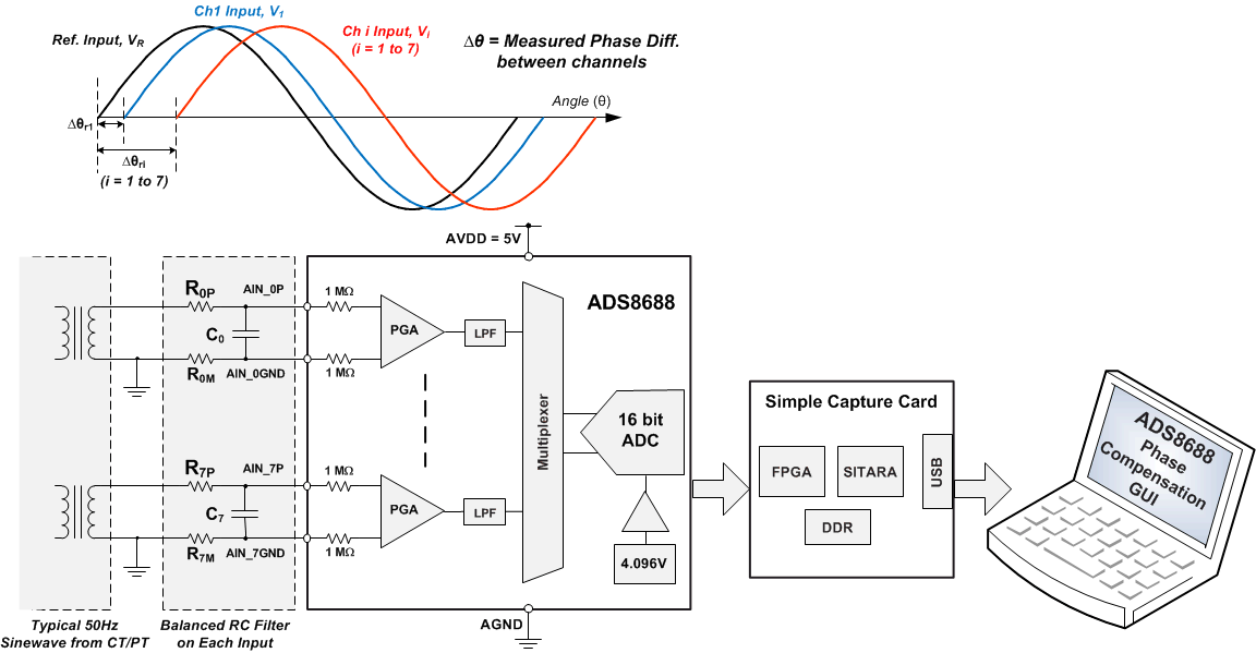
9.2.1 Phase-Compensated, 8-Channel, Multiplexed Data Acquisition System for Power Automation
 Figure 95. 8-Channel, Multiplexed Data Acquisition System for Power Automation
9.2.1.1 Design Requirements
In modern power grids, accurately measuring the electrical parameters of the various areas of the power grid is extremely critical. This measurement helps determine the operating status and running quality of the grid. Such accurate measurements also help diagnose potential problems with the power network so that these problems can be resolved quickly without having any significant service impact. The key electrical parameters include amplitude, frequency, and phase, which are important for calculating the power factor, power quality, and other parameters of the power system.
The phase angle of the electrical signal on the power network buses is a special interest to power system engineers. The primary objective for this design is to accurately measure the phase and phase difference between the analog input signals in a multichannel data acquisition system. When multiple input channels are sampled in a sequential manner as in a multiplexed ADC, an additional phase delay is introduced between the channels. Thus the phase measurements are not accurate. However, this additional phase delay is constant and can be compensated in application software.
The key design requirements are given below:
- Single-ended sinusoidal input signal with a ±10-V amplitude and typical frequency (fIN = 50 Hz).
- Design an 8-channel multiplexed data acquisition system using a 16-bit SAR ADC.
- Design a software algorithm to compensate for the additional phase difference between the channels.
9.2.1.2 Detailed Design Procedure
The application circuit and system diagram for this design is shown in Figure 95. This design includes a complete hardware and software implementation of a multichannel data acquisition system for power automation applications.
The system hardware uses the ADS8688, which is a 16-bit, 500-kSPS, 8-channel, multiplexed input, SAR ADC with integrated precision reference and analog front-end circuitry for each channel. The ADC supports bipolar input ranges up to ±10.24 V with a single 5-V supply and provides minimum latency in data output resulting from the SAR architecture. The integration offered by this device makes the ADS8684 and ADS8688 an ideal selection for such applications, because the integrated signal conditioning helps minimize system components and avoids the need for generating high-voltage supply rails. The overall system-level dc precision (gain and offset errors) and low temperature drift offered by this device helps system designers achieve the desired system accuracy without calibration. In most applications, using passive RC filters or multi-stage filters in front of the ADC is preferred to reduce the noise of the input signal.
The software algorithm implemented in this design uses the discrete fourier transform (DFT) method to calculate and track the input signal frequency, get the exact phase angle of the individual signal, calculate the phase difference, and implement phase compensation. The entire algorithm has four steps:
- Calculate the theoretical phase difference introduced by the ADC resulting from multiplexing input channels.
- Estimate the frequency of the input signal using frequency tracking and DFT techniques.
- Calculate the phase angle of all signals in the system based on the estimated frequency.
- Compensate the phase difference for all channels using the theoretical value of an additional MUX phase delay calculated in the first step.
9.2.1.3 Application Curve
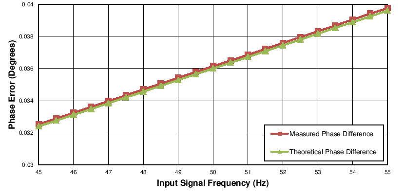
The performance summary for this design is summarized in Table 17 and Figure 96. In this example, multiple sinusoidal input signals of amplitude ±10 V are applied to the inputs of the ADC. The initial phase angle is the same for all signals, but the input frequency is varied from 45 Hz to 55 Hz. The phase error in the last column of Table 17 reflects the measurement accuracy of this design.
Table 17. Theoretical and Measured Phase Difference
| INPUT TEST CONDITION | THEORETICAL PHASE ERROR(1) | MEASURED PHASE ERROR(2) | PHASE ERROR AFTER COMPENSATION(3) |
|---|---|---|---|
| Phase difference (consecutive channels) |
0.036° | 0.036145° | 0.000145° |
| Phase difference (farthest channels, channel 0 to channel 7) |
0.252° | 0.249964° | 0.002036° |
 Figure 96. Measured and Theoretical Phase Difference Between Consecutive Channels
 |
For a step-by-step design procedure, circuit schematics, bill of materials, PCB files, simulation results, and test results, refer to Phase Compensated 8-Channel, Multiplexed Data Acquisition System for Power Automation Reference Design (TIDU427). |
9.2.2 16-Bit, 8-Channel, Integrated Analog Input Module for Programmable Logic Controllers (PLCs)
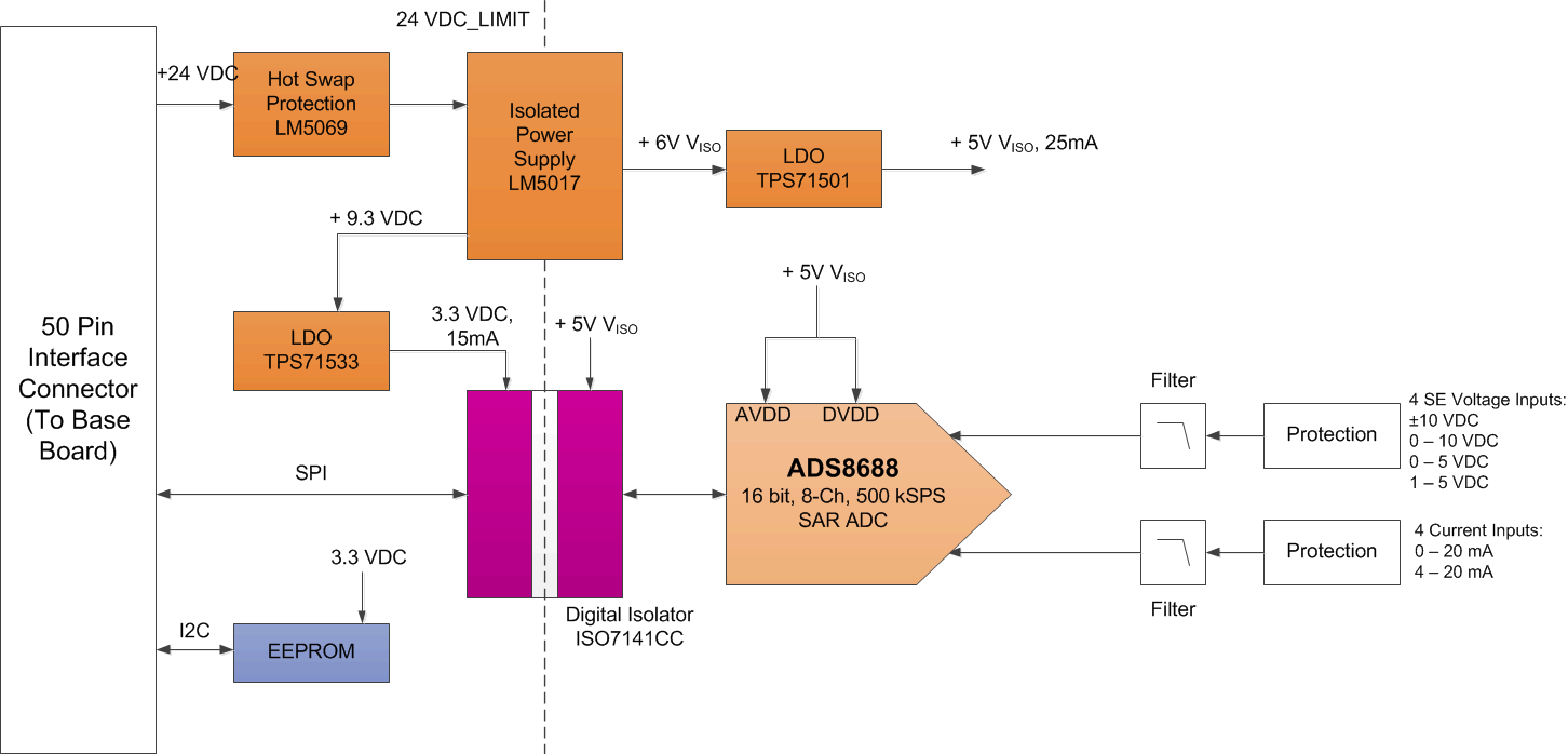
 Figure 97. 16-Bit, 8-Channel, Integrated Analog Input Module for PLCs
9.2.2.1 Design Requirements
This reference design provides a complete solution for a single-supply industrial control analog input module. The design is suitable for process control end equipment such as programmable logic controllers (PLCs), distributed control systems (DCS) and data acquisition systems (DAS) modules that must digitize standard industrial current inputs, and bipolar or unipolar input voltage ranges up to ±10 V. In an industrial environment, the analog voltage and current ranges typically include ±2.5 V, ±5 V, ±10 V, 0 V to 5 V, 0 V to 10 V, 4 mA to
20 mA, and 0 mA to 20 mA. This reference design can measure all standard industrial voltage and current inputs. Eight channels are provided on the module, and each channel can be configured as a current or voltage input with software configuration.
The key design requirements are given below:
- Up to eight channels of user-programmable inputs:
- Voltage inputs (with a typical ZIN of 1 MΩ): ±10 V, ±5 V, ±2.5 V, 0 V to 10 V and 0 V to 5 V.
- Current inputs (with a ZIN of 300 Ω): 0 mA to 20 mA, 4 mA to 20 mA, and ±20 mA.
- A 16-bit SAR ADC with SPI.
- Accuracy of ≤ 0.2% at 25°C over entire input range of voltage and current inputs.
- Onboard isolated Fly-Buck™ power supply with inrush current protection.
- Slim-form factor 96 × 50.8 × 10 mm (L × W × H).
- LabView-based GUI for signal-chain analysis and functional testing.
- Designed to comply with IEC61000-4 standards for ESD, EFT, and surge.
9.2.2.2 Detailed Design Procedure
The application circuit and system diagram for this design is shown in Figure 97.
The module has eight analog input channels, and each channel can be configured as a current or voltage input with software configuration. The design uses the ADS8688 (16-bit, 8-channel, single-supply SAR ADC) with an on-chip PGA and reference. The on-chip PGA provides a high-input impedance (typically 1 MΩ) and filters noise interference. The on-chip, 4.096-V, ultra-low drift voltage reference is used as the reference for the ADC core.
The digital isolation is achieved using an ISO7141CC and ISO1541D. The host microcontroller communicates with a TCA6408A (an 8-bit, I2C, I/O expander over an I2C bus). The ISO1541D is a bidirectional, I2C isolator that isolates the I2C lines for the TCA6408A. The TCA6408A controls the low RON opto-switch (TLP3123), which is used to switch between voltage-to-current input modes. The input channel configuration is done in microcontroller firmware.
A low-cost, constant, on-time, synchronous buck regulator in fly-buck configuration with an external transformer (LM5017) generates the isolated power supply. The LM5017 has a wide input supply range, making this device ideal for accepting a 24-V industrial supply. This transformer can accept up to 100 V, thereby making reliable transient protection of the input supply more easily achievable. The fly-buck power supply isolates and steps the input voltage down to 6 V. The supply then provides that voltage to the TPS70950 (the low dropout regulator) to generate 5 V to power the ADS8688 and other circuitry. The LM5017 also features a number of other safety and reliability functions, such as undervoltage lockout (UVLO), thermal shutdown, and peak current limit protection.
Input analog signals are protected against high-voltage, fast-transient events often expected in an industrial environment. The protection circuitry makes use of the transient voltage suppressor (TVS) and ESD diodes. The RC low-pass mode filters are used on each analog input before the input reaches the ADS8688, which eliminates any high-frequency noise pickups and minimizes aliasing.
9.2.2.3 Application Curve
The performance summary for this design is summarized in Table 18.
Table 18. Measurement Results Summary for PLC Analog Input Module Design
| SERIAL NUMBER | PARAMETER | INPUT RANGE | ADS8688 SPECIFICATION | MEASURED RESULT |
|---|---|---|---|---|
| 1 | SNR (dB) | ±10 V | 90 dB (min) | 90.85 dB |
| 0 V 10 V | 88.5 dB (min) | 89.52 dB | ||
| 0 V to 5 V | 87.5 dB (min) | 88.48 dB | ||
| 2 | ENOB (Bits) | ±10 V | 14.66 | 14.80 |
| 0 V 10 V | 14.41 | 14.58 | ||
| 0 V to 5 V | 14.24 | 14.41 | ||
| 3 | Maximum INL (LSB) | ±10 V | 2 | 1.77 |
| 0 V 10 V | 2 | 1.64 | ||
| 0 V to 5 V | 2 | 1.35 | ||
| 4 | Minimum INL (LSB) | ±10 V | –2 | –1.47 |
| 0 V 10 V | –2 | –1.36 | ||
| 0 V to 5 V | –2 | –1.37 |
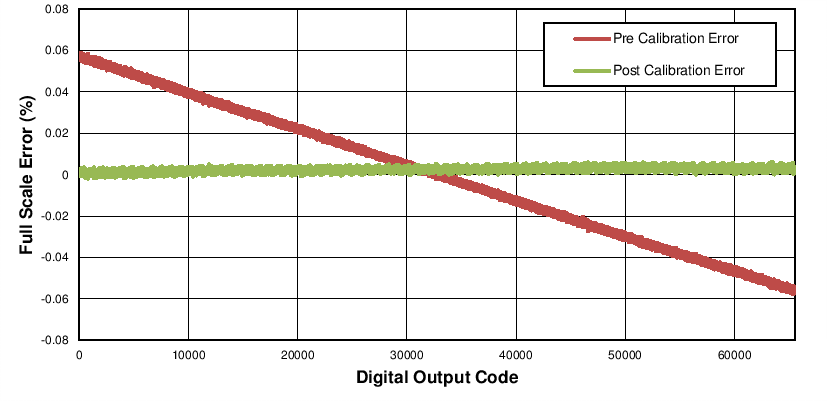
The accuracy performance for this design for the ±10.24-V input range is shown in Figure 98.
 Figure 98. System Accuracy Performance in ±2.5 × VREF Input Range
 |
For a step-by-step design procedure, circuit schematics, bill of materials, PCB files, simulation results, and test results, refer to 16-Bit, 8-Channel, Integrated Analog Input Module for Programmable Logic Controllers (PLCs) (TIDU365). |