SBAS614C May   2013  – March 2019 ADS8866

PRODUCTION DATA.  

  1. Features
  2. Applications
  3. Description
    1.     Device Images
      1.      No Separate LDO Required for the ADC Supply
  4. Revision History
  5. Device Comparison Table
  6. Pin Configuration and Functions
    1.     Pin Functions
  7. Specifications
    1. 7.1 Absolute Maximum Ratings
    2. 7.2 ESD Ratings
    3. 7.3 Recommended Operating Conditions
    4. 7.4 Thermal Information
    5. 7.5 Electrical Characteristics
    6. 7.6 Timing Requirements: 3-Wire Operation
    7. 7.7 Timing Requirements: 4-Wire Operation
    8. 7.8 Timing Requirements: Daisy-Chain
    9. 7.9 Typical Characteristics
  8. Parameter Measurement Information
    1. 8.1 Equivalent Circuits
  9. Detailed Description
    1. 9.1 Overview
    2. 9.2 Functional Block Diagram
    3. 9.3 Feature Description
      1. 9.3.1 Analog Input
      2. 9.3.2 Reference
      3. 9.3.3 Clock
      4. 9.3.4 ADC Transfer Function
    4. 9.4 Device Functional Modes
      1. 9.4.1 CS Mode
        1. 9.4.1.1 3-Wire CS Mode
        2. 9.4.1.2 4-Wire CS Mode
      2. 9.4.2 Daisy-Chain Mode
        1. 9.4.2.1 Daisy-Chain Mode
  10. 10Application and Implementation
    1. 10.1 Application Information
      1. 10.1.1 ADC Reference Driver
      2. 10.1.2 ADC Input Driver
        1. 10.1.2.1 Input Amplifier Selection
        2. 10.1.2.2 Charge-Kickback Filter
    2. 10.2 Typical Applications
      1. 10.2.1 DAQ Circuit for a 10-µs, Full-Scale Step Response
        1. 10.2.1.1 Design Requirements
        2. 10.2.1.2 Detailed Design Procedure
      2. 10.2.2 DAQ Circuit for Lowest Distortion and Noise Performance at 100 kSPS
        1. 10.2.2.1 Design Requirements
        2. 10.2.2.2 Detailed Design Procedure
      3. 10.2.3 Ultralow-Power DAQ Circuit at 10 kSPS
        1. 10.2.3.1 Design Requirements
        2. 10.2.3.2 Detailed Design Procedure
  11. 11Power Supply Recommendations
    1. 11.1 Power-Supply Decoupling
    2. 11.2 Power Saving
  12. 12Layout
    1. 12.1 Layout Guidelines
    2. 12.2 Layout Example
  13. 13Device and Documentation Support
    1. 13.1 Documentation Support
      1. 13.1.1 Related Documentation
    2. 13.2 Receiving Notification of Documentation Updates
    3. 13.3 Community Resources
    4. 13.4 Trademarks
    5. 13.5 Electrostatic Discharge Caution
    6. 13.6 Glossary
  14. 14Mechanical, Packaging, and Orderable Information

Package Options

Mechanical Data (Package|Pins)
Thermal pad, mechanical data (Package|Pins)
Orderable Information

ADC Transfer Function

The ADS8866 is a unipolar, single-ended input device. The device output is in straight binary format.

Figure 42 shows ideal characteristics for the device. The full-scale range for the ADC input (AINP – AINN) is equal to the reference input voltage to the ADC (VREF). One LSB is equal to [(VREF / 216)].
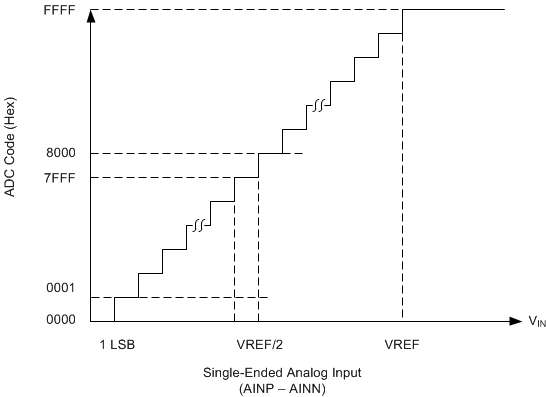
ADS8866 ai_transfer_chara_se_bas557.gifFigure 42. Single-Ended Transfer Characteristics