SBAS728A November 2016 – June 2017 ADS8900B , ADS8902B , ADS8904B
PRODUCTION DATA.
- 1 Features
- 2 Applications
- 3 Description
- 4 Revision History
- 5 Pin Configuration and Functions
- 6 Specifications
-
7 Detailed Description
- 7.1 Overview
- 7.2 Functional Block Diagram
- 7.3 Feature Description
- 7.4 Device Functional Modes
- 7.5
Programming
- 7.5.1 Output Data Word
- 7.5.2 Data Transfer Frame
- 7.5.3 Interleaving Conversion Cycles and Data Transfer Frames
- 7.5.4 Data Transfer Protocols
- 7.5.5 Device Setup
- 7.6
Register Maps
- 7.6.1
Device Configuration and Register Maps
- 7.6.1.1 PD_CNTL Register (address = 04h) [reset = 00h]
- 7.6.1.2 SDI_CNTL Register (address = 008h) [reset = 00h]
- 7.6.1.3 SDO_CNTL Register (address = 0Ch) [reset = 00h]
- 7.6.1.4 DATA_CNTL Register (address = 010h) [reset = 00h]
- 7.6.1.5 PATN_LSB Register (address = 014h) [reset = 00h]
- 7.6.1.6 PATN_MID Register (address = 015h) [reset = 00h]
- 7.6.1.7 PATN_MSB Register (address = 016h) [reset = 00h]
- 7.6.1.8 OFST_CAL Register (address = 020h) [reset = 00h]
- 7.6.1.9 REF_MRG Register (address = 030h) [reset = 00h]
- 7.6.1
Device Configuration and Register Maps
-
8 Application and Implementation
- 8.1 Application Information
- 8.2 Typical Application
- 9 Power-Supply Recommendations
- 10Layout
- 11Device and Documentation Support
- 12Mechanical, Packaging, and Orderable Information
Package Options
Mechanical Data (Package|Pins)
- RGE|24
Thermal pad, mechanical data (Package|Pins)
- RGE|24
Orderable Information
10 Layout
10.1 Layout Guidelines
This section provides some layout guidelines for achieving optimum performance with the ADS890xB device family.
10.1.1 Signal Path
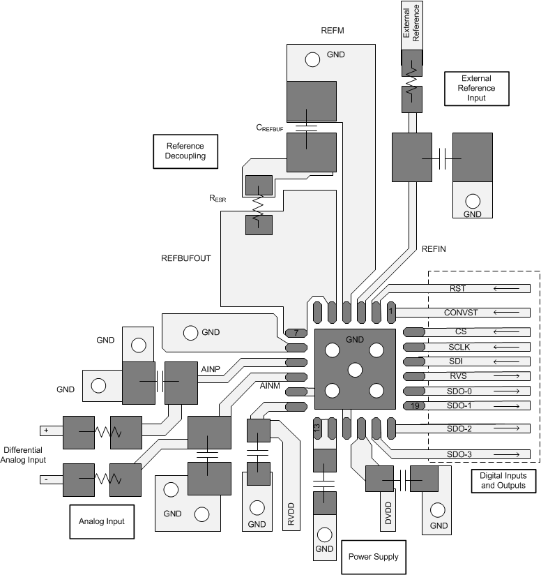
As illustrated in Figure 121, the analog input signals are routed in opposite directions to the digital connections. The reference decoupling components are kept away from the switching digital signals. This arrangement prevents noise generated by digital switching activity from coupling to sensitive analog signals.
10.1.2 Grounding and PCB Stack-Up
Low inductance grounding is critical for achieving optimum performance. Grounding inductance is kept below 1 nH with 15-mil grounding vias and a printed circuit board (PCB) layout design that has at least four layers. Place all critical components of the signal chain on the top layer with a solid analog ground from subsequent inner layers to minimize via length to ground.
For lowest inductance grounding, connect the GND pins of the ADS890xB (pin 11 and pin 15) directly to the device thermal pad and place at least four 8-mil grounding vias on the device thermal pad.
10.1.3 Decoupling of Power Supplies
Place the decoupling capacitors on RVDD, the LDO output, and DVDD within 20 mil from the respective pins, and use a 15-mil via to ground from each capacitor. Avoid placing vias between any supply pin and the respective decoupling capacitor.
10.1.4 Reference Decoupling
Dynamic currents are also present at the REFBUFOUT and REFM pins during the conversion phase, and excellent decoupling is required to achieve optimum performance. Place a 22-μF, X7R-grade, ceramic capacitor with at least 10-V rating and an ESR of 1-Ω between the REFBUFOUT and the REFM pins, as illustrated in Figure 121. Select 0603- or 0805-size capacitors to keep equivalent series inductance (ESL) low. Connect the REFM pins to the decoupling capacitor before a ground via.
10.1.5 Differential Input Decoupling
Dynamic currents are also present at the differential analog inputs of the ADS890xB. Use C0G- or NPO-type capacitors to decouple these inputs because with these type of capacitors, capacitance stays almost constant over the full input voltage range. Lower-quality capacitors (such as X5R and X7R) have large capacitance changes over the full input-voltage range that may cause degradation in the performance of the device.
10.2 Layout Example
 Figure 121. Recommended Layout