SBOS588B December 2011 – June 2019 AFE030
PRODUCTION DATA.
- 1 Features
- 2 Applications
- 3 Description
- 4 Revision History
- 5 Description, continued
- 6 Pin Configuration and Functions
-
7 Specifications
- 7.1 Absolute Maximum Ratings
- 7.2 ESD Ratings
- 7.3 Thermal Information
- 7.4 Electrical Characteristics: Transmitter (Tx), Tx_DAC
- 7.5 Electrical Characteristics: Transmitter (Tx), Tx_PGA
- 7.6 Electrical Characteristics: Transmitter (Tx), Tx_FILTER
- 7.7 Electrical Characteristics: Power Amplifier (PA)
- 7.8 Electrical Characteristics: Receiver (Rx), Rx PGA1
- 7.9 Electrical Characteristics: Receiver (Rx), Rx Filter
- 7.10 Electrical Characteristics: Receiver (Rx), Rx PGA2
- 7.11 Electrical Characteristics: Digital
- 7.12 Electrical Characteristics: Two-Wire Interface
- 7.13 Electrical Characteristics: Zero-Crossing Detector
- 7.14 Electrical Characteristics: Internal Bias Generator
- 7.15 Electrical Characteristics: Power Supply
- 7.16 Typical Characteristics
- 8 Parameter Measurement Information
- 9 Detailed Description
- 10Application and Implementation
- 11Device and Documentation Support
Package Options
Mechanical Data (Package|Pins)
- RGZ|48
Thermal pad, mechanical data (Package|Pins)
- RGZ|48
Orderable Information
9.3.2 Tx Block
The Tx block consists of the Tx PGA and Tx Filter. The Tx PGA is a low-noise, high-performance, programmable gain amplifier. In DAC mode (where pin 7 is a logical '1' and Enable1 Register bit location 5 is a logical '1'), the Tx PGA operates as the internal digital-to-analog converter (DAC) output buffer with programmable gain. In PWM mode (where pin 7 is a logical '0' and Enable1 Register bit location 5 is a logical '0'), the Tx PGA operates as a stand-alone programmable gain amplifier. The Tx PGA gain is programmed through the serial interface. The Tx PGA gain settings are 0.25 V/V, 0.5 V/V, 0.707 V/V, and 1 V/V.
The Tx Filter is a unity-gain, fourth-order low-pass filter. The Tx Filter cutoff frequency is selectable between CENELEC A or CENELEC B, C, and D modes. The Control1 Register bit location 3 setting (CA CBCD) determines the cutoff frequency. Setting Control1 Register bit location 3 to '0' selects the CENELEC A band; setting Control1 Register bit location 3 to '1' selects CENELEC B, C, and D bands.
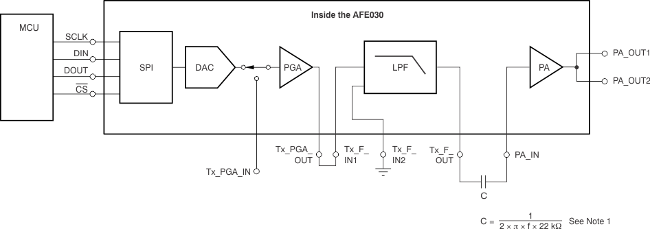
The AFE030 supports both DAC inputs or PWM inputs for the Tx signal path. DAC mode is recommended for best performance. In DAC mode, no external components in the Tx signal path are required to meet regulatory signal emissions requirements. When in DAC mode, the AFE030 accepts serial data from the microprocessor and writes that data to the internal DAC registers. When in DAC mode (where pin 7 is a logical '1' and Enable1 Register bit location 5 is a logical '1'), the Tx PGA output must be directly coupled to the Tx_FIN1 input and the unused Tx_FIN2 input must be grounded.
The proper connections for the Tx signal path for DAC mode operation are shown in Figure 27. Operating in DAC mode results in the lowest distortion signal injected onto the ac mains. No additional external filtering components are required to meet CENELEC requirements for A, B, C or D bands when operating in DAC mode.
NOINDENT:
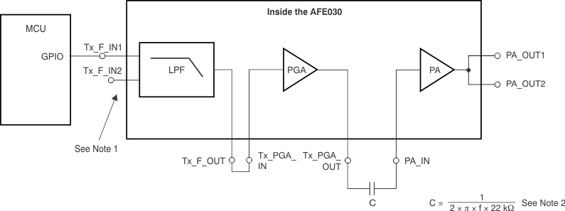
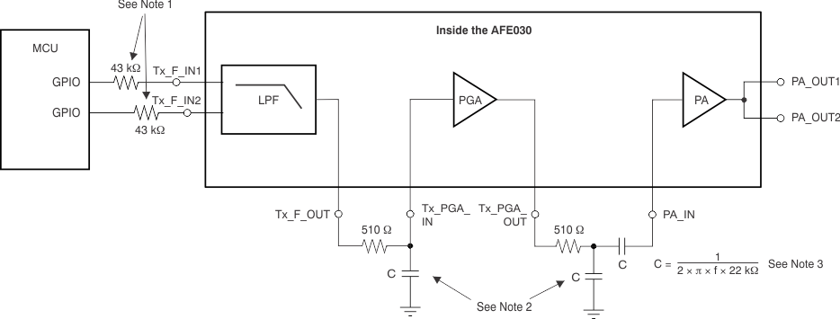
For capacitor value C, f is the desired lower cutoff frequency and 22 kΩ is the PA input resistance.In PWM mode (where pin 7 is a logical '0' and Enable1 Register bit location 5 is a logical '0'), the microprocessor general-purpose input/output (GPIO) can be connected directly to either one of the Tx Filter inputs; the unused input should remain unconnected. A lower distortion PWM signal generated from two PWM signals shifted in phase by 90 degrees can be also be input to the Tx Filter through the use of both inputs. Figure 28 and Figure 29 show the proper connections for single PWM and dual PWM operating modes, respectively.
NOINDENT:
Leave unused Tx Filter input unconnected.NOINDENT:
For capacitor value C, f is the desired lower cutoff frequency and 22 kΩ is the PA input resistance.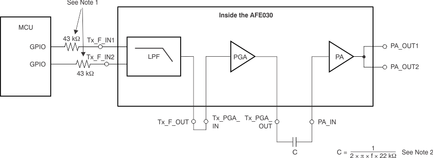
NOINDENT:
When using both Tx Filter inputs, use 43-kΩ resistors to match the input resistance for best frequency response.NOINDENT:
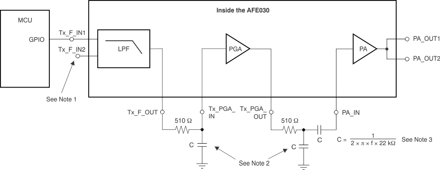
For capacitor value C, f is the desired lower cutoff frequency and 22 kΩ is the PA input resistance.In PWM mode, there is inherently more distortion from the PWM signal than from the internal DAC. To achieve the best results in PWM mode, add passive RC filters to increase the low-pass filtering. Figure 30 and Figure 31 illustrate the recommended locations of these RC filters.
NOINDENT:
Leave unused Tx Filter input unconnected.NOINDENT:
For capacitor value C, f is the desired lower cutoff frequency and 22 kΩ is the PA input resistance.Using One PWM Signal and Additional RC Filters
NOINDENT:
When using both Tx Filter inputs, use 43-kΩ resistors to match the input resistance for best frequency response.NOINDENT:
For capacitor value C, f is the desired lower cutoff frequency and 22 kΩ is the PA input resistance.Using Two PWM Signals and Additional RC Filters
For the capacitors listed in Table 3, it is recommended that these components be rated to withstand the full AVDD power-supply voltage.
Table 3. Recommended External R and C Values to Increase Tx Filter Response Order in PWM Applications
| FREQUENCY BAND | R (Ω) | C (nF) |
|---|---|---|
| SFSK: 63 kHz, 74 kHz | 510 | 2.7 |
| CENELEC A | 510 | 1.5 |
| CENELEC B, C, D | 510 | 1 |
The Tx PGA and Tx Filter each have the inputs and outputs externally available in order to provide maximum system design flexibility. Care should be taken when laying out the PCB traces from the inputs or outputs to avoid excessive capacitive loading. Keeping the PCB capacitance from the inputs to ground, or from the outputs to ground, less than 100 pF is recommended.