SLOS729D October 2011 – November 2015 AFE5808A
PRODUCTION DATA.
- 1 Features
- 2 Applications
- 3 Description
- 4 Revision History
- 5 Description (continued)
- 6 Pin Configuration and Functions
- 7 Specifications
-
8 Detailed Description
- 8.1 Overview
- 8.2 Functional Block Diagram
- 8.3 Feature Description
- 8.4 Device Functional Modes
- 8.5 Programming
- 8.6
Register Maps
- 8.6.1 ADC Register Map
- 8.6.2
ADC Register/Digital Processing Description
- 8.6.2.1 AVERAGING_ENABLE: Address: 2[11]
- 8.6.2.2 ADC_OUTPUT_FORMAT: Address: 4[3]
- 8.6.2.3 DIGITAL_GAIN_ENABLE: Address: 3[12]
- 8.6.2.4 DIGITAL_HPF_ENABLE
- 8.6.2.5 DIGITAL_HPF_FILTER_K_CHX
- 8.6.2.6 LOW_FREQUENCY_NOISE_SUPPRESSION: Address: 1[11]
- 8.6.2.7 LVDS_OUTPUT_RATE_2X: Address: 1[14]
- 8.6.2.8 CHANNEL_OFFSET_SUBSTRACTION_ENABLE: Address: 3[8]
- 8.6.2.9 SERIALIZED_DATA_RATE: Address: 3[14:13]
- 8.6.2.10 TEST_PATTERN_MODES: Address: 2[15:13]
- 8.6.2.11 SYNC_PATTERN: Address: 10[8]
- 8.6.3 VCA Register Map
- 8.6.4 AFE5808A VCA Register Description
-
9 Application and Implementation
- 9.1 Application Information
- 9.2 Typical Application
- 9.3
Do's and Don'ts
- 9.3.1 Driving the Inputs (Analog or Digital) Beyond the Power-Supply Rails
- 9.3.2 Driving the Device Signal Input With an Excessively High Level Signal
- 9.3.3 Driving the VCNTL Signal With an Excessive Noise Source
- 9.3.4 Using a Clock Source With Excessive Jitter, an Excessively Long Input Clock Signal Trace, or Having Other Signals Coupled to the ADC or CW Clock Signal Trace
- 9.3.5 LVDS Routing Length Mismatch
- 9.3.6 Failure to Provide Adequate Heat Removal
- 10Power Supply Recommendations
- 11Layout
- 12Device and Documentation Support
- 13Mechanical, Packaging, and Orderable Information
Package Options
Mechanical Data (Package|Pins)
- ZCF|135
Thermal pad, mechanical data (Package|Pins)
Orderable Information
8 Detailed Description
8.1 Overview
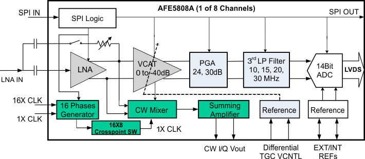
The AFE5808A device is a highly integrated analog front-end (AFE) solution specifically designed for ultrasound systems in which high performance and small size are required. The AFE5808A device integrates a complete time-gain-control (TGC) imaging path and a continuous wave doppler (CWD) path. This device also enables users to select one of various power/noise combinations to optimize system performance. The AFE5808A device contains eight channels; each channel includes a low-noise amplifier (LNA), voltage controlled attenuator (VCAT), programmable gain amplifier (PGA), low-pass filter (LPF), 14-bit analog-to-digital converter (ADC), and CW mixer.
In addition, multiple features in the AFE5808A device are suitable for ultrasound applications, such as active termination, individual channel control, fast power-up and power-down response, programmable clamp voltage control, fast and consistent overload recovery, and so forth. Therefore the AFE5808A device brings premium image quality to ultra–portable, handheld systems all the way up to high-end ultrasound systems. See Functional Block Diagram.
8.2 Functional Block Diagram
8.3 Feature Description
8.3.1 Low-Noise Amplifier (LNA)
In many high-gain systems, a low noise amplifier is critical for achieving overall performance. Using a new proprietary architecture, the LNA in the AFE5808A device delivers exceptional low-noise performance, while operating on a low quiescent current compared to CMOS-based architectures with similar noise performance. The LNA performs single-ended input to differential output voltage conversion. The LNA is configurable for a programmable gain of 24 dB, 18 dB, and 12 dB, and its input-referred noise is only 0.63 nV/√Hz 0.70 nV/√Hz, and 0.9 nV/√Hz respectively. Programmable gain settings result in a flexible linear input range up to 1 VPP, realizing high signal handling capability demanded by new transducer technologies. Larger input signal can be accepted by the LNA; however the signal can be distorted since it exceeds the LNA’s linear operation region. Combining the low noise and high input range, a wide input dynamic range is achieved consequently for supporting the high demands from various ultrasound imaging modes.
The LNA input is internally biased at approximately 2.4 V; the signal source should be AC-coupled to the LNA input by an adequately-sized capacitor, for example, ≥ 0.1 µF. To achieve low DC offset drift, the AFE5808A device incorporates a DC offset correction circuit for each amplifier stage. To improve the overload recovery, an integrator circuit is used to extract the DC component of the LNA output and then fed back to the LNA’s complementary input for DC offset correction. This DC offset correction circuit has a high-pass response and can be treated as a high-pass filter. The effective corner frequency is determined by the capacitor CBYPASS connected at INM. With larger capacitors, the corner frequency is lower. For stable operation at the highest HP filer cut-off frequency, a ≥ 15-nF capacitor can be selected. This corner frequency scales almost linearly with the value of the CBYPASS. For example, 15 nF gives a corner frequency of approximately 100 kHz, while 47 nF can give an effective corner frequency of 33 kHz. The DC offset correction circuit can also be disabled or enabled through register 52[12].
The AFE5808A device can be terminated passively or actively. Active termination is preferred in ultrasound application for reducing reflection from mismatches and achieving better axial resolution without degrading the noise figure too much. Active termination values can be preset to 50 Ω, 100 Ω, 200 Ω, and 400 Ω; other values also can be programmed by users through register 52[4:0]. A feedback capacitor is required between ACTx and the signal source as Figure 59 shows. On the active termination path, a clamping circuit is also used to create a low impedance path when overload signal is seen by the AFE5808A device. The clamp circuit limits large input signals at the LNA inputs, and it improves the overload recovery performance of the AFE5808A device. The clamp level can be set to 350 mVPP, 600 mVPP, and 1.15 VPP automatically depending on the LNA gain settings when register 52[10:9] = 0. Other clamp voltages, such as 1.15 VPP, 0.6 VPP, and 1.5 VPP, are also achievable by setting register 52[10:9]. This clamping circuit is also designed to obtain good pulse inversion performance and reduce the impact from asymmetric inputs.
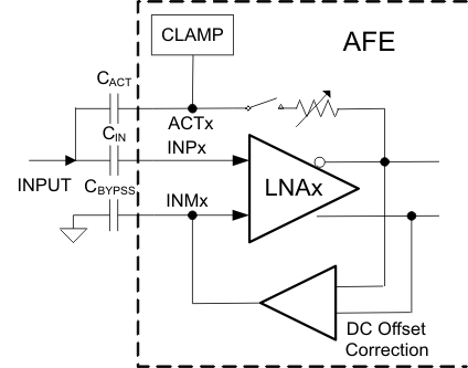 Figure 59. AFE5808A LNA With DC Offset Correction Circuit
8.3.2 Voltage-Controlled Attenuator
The voltage-controlled attenuator is designed to have a linear-in-dB attenuation characteristic; that is, the average gain loss in dB (see Figure 2) is constant for each equal increment of the control voltage (VCNTL) as shown in Figure 60. A differential control structure is used to reduce common mode noise. A simplified attenuator structure is shown in the following Figure 60 and Figure 61.
The attenuator is essentially a variable voltage divider that consists of the series input resistor (RS) and seven shunt FETs placed in parallel and controlled by sequentially activated clipping amplifiers (A1 through A7). VCNTL is the effective difference between VCNTLP and VCNTLM. Each clipping amplifier can be understood as a specialized voltage comparator with a soft transfer characteristic and well-controlled output limit voltage. Reference voltages V1 through V7 are equally spaced over the 0-V to 1.5-V control voltage range. As the control voltage increases through the input range of each clipping amplifier, the amplifier output rises from a voltage where the FET is nearly OFF to VHIGH where the FET is completely ON. As each FET approaches its ON state and the control voltage continues to rise, the next clipping amplifier/FET combination takes over for the next portion of the piecewise-linear attenuation characteristic. Thus, low control voltages have most of the FETs turned OFF, producing minimum signal attenuation. Similarly, high control voltages turn the FETs ON, leading to maximum signal attenuation. Therefore, each FET acts to decrease the shunt resistance of the voltage divider formed by Rs and the parallel FET network.
Additionally, a digitally controlled TGC mode is implemented to achieve better phase-noise performance in the AFE5808A device. The attenuator can be controlled digitally instead of the analog control voltage VCNTL. This mode can be set by the register bit 59[7]. The variable voltage divider is implemented as a fixed series resistance and FET as the shunt resistance. Each FET can be turned ON by connecting the switches SW1-7. Turning on each of the switches can give approximately 6 dB of attenuation, which can be controlled by the register bits 59[6:4]. This digital control feature can eliminate the noise from the VCNTL circuit and ensures the better SNR and phase noise for TGC path.
 Figure 60. Simplified Voltage Controlled Attenuator (Analog Structure)
 Figure 61. Simplified Voltage Controlled Attenuator (Digital Structure)
The voltage controlled attenuator noise follows a monotonic relationship to the attenuation coefficient. At higher attenuation, the input-referred noise is higher and conversely. The attenuator noise is then amplified by the PGA and becomes the noise floor at the ADC input. In the attenuator’s high attenuation operating range, that is VCNTL is high, the attenuator input noise may exceed the LNA’s output noise; the attenuator then becomes the dominant noise source for the following PGA stage and ADC. Therefore the attenuator’s noise should be minimized compared to the LNA output noise. The AFE5808A’s attenuator is designed for achieving low noise even at high attenuation (low channel gain) and realizing better SNR in the near field. Table 1 shows the input referred noise for different attenuations.
Table 1. Voltage-Controlled-Attenuator Noise vs Attenuation
| ATTENUATION (dB) | ATTENUATOR INPUT REFERRED NOISE (nV/√Hz) |
|---|---|
| –40 | 10.5 |
| –36 | 10 |
| –30 | 9 |
| –24 | 8.5 |
| –18 | 6 |
| –12 | 4 |
| –6 | 3 |
| 0 | 2 |
8.3.3 Programmable Gain Amplifier
After the voltage controlled attenuator, a programmable gain amplifier (PGA) can be configured as 24 dB or 30 dB with a constant input referred noise of 1.75 nV/√Hz. The PGA structure consists of a differential voltage-to-current converter with programmable gain, current clamp (bias control) circuits, a transimpedance amplifier with a programmable low-pass filter, and a DC offset correction circuit. See Figure 62 for the simplified block diagram of the PGA.
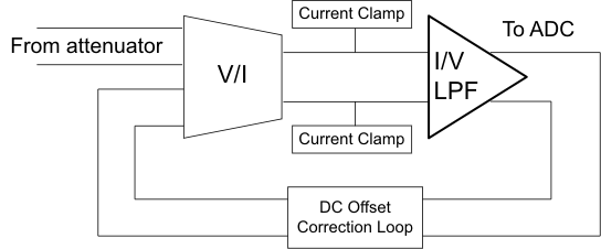 Figure 62. Simplified Block Diagram of PGA
Low input noise is always preferred in a PGA because its noise contribution should not degrade the ADC SNR too much after the attenuator. At the minimum attenuation (used for small input signals), the LNA noise dominates; at the maximum attenuation (large input signals), the PGA and ADC noise dominates. Thus 24-dB gain of PGA achieves better SNR as long as the amplified signals can exceed the noise floor of the ADC.
The PGA current clamp circuit can be enabled (register 51) to improve the overload recovery performance of the AFE. If we measure the standard deviation of the output just after overload, for 0.5 V VCNTL, it is about 3.2 LSBs in normal case (that is, the output is stable in about 1 clock cycle after overload). With the current clamp circuit disabled, the value approaches 4 LSBs, meaning a longer time duration before the output stabilizes; however, with the current clamp circuit enabled, there will be degradation in HD3 for PGA output levels > –2dBFS. For example, for a –2-dBFS output level, the HD3 degrades by approximately 3 dB. To maximize the output dynamic range, the maximum PGA output level can be above 2 VPP even with the clamp circuit enabled; the ADC in the AFE has excellent overload recovery performance to detect small signals right after the overload.
NOTE
In the low power and medium power modes, PGA_CLAMP is disabled for saving power if 51[7] = 0.
The AFE5808A device integrates an anti-aliasing filter in the form of a programmable low-pass filter (LPF) in the transimpedance amplifier. The LPF is designed as a differential, active, 3rd order filter with a typical 18 dB-per-octave roll-off. Programmable through the serial interface, the –1-dB frequency corner can be set to one of 10 MHz, 15 MHz, 20 MHz, and 30 MHz. The filter bandwidth is set for all channels simultaneously.
A selectable DC offset correction circuit is implemented in the PGA as well. This correction circuit is similar to the one used in the LNA. The circuit extracts the DC component of the PGA outputs and feeds back to the PGA’s complimentary inputs for DC offset correction. This DC offset correction circuit also has a high-pass response with a cut-off frequency of 80 KHz.
8.3.4 Analog-to-Digital Converter
The analog-to-digital converter (ADC) of the AFE5808A device employs a pipelined converter architecture that consists of a combination of multi-bit and single-bit internal stages. Each stage feeds its data into the digital error correction logic, ensuring excellent differential linearity and no missing codes at the 14-bit level. The 14 bits given out by each channel are serialized and sent out on a single pair of pins in LVDS format. All eight channels of the AFE5808A device operate from a common input clock (CLKP/M). The sampling clocks for each of the eight channels are generated from the input clock using a carefully matched clock buffer tree. The 14x clock required for the serializer is generated internally from the CLKP/M pins. A 7x and a 1x clock are also given out in LVDS format, along with the data, to enable easy data capture. The AFE5808A device operates from internally-generated reference voltages that are trimmed to improve the gain matching across devices. The nominal values of REFP and REFM are 1.5 V and 0.5 V, respectively. Alternately, the device also supports an external reference mode that can be enabled using the serial interface.
Using serialized LVDS transmission has multiple advantages, such as a reduced number of output pins (saving routing space on the board), reduced power consumption, and reduced effects of digital noise coupling to the analog circuit inside the AFE5808A device.
8.3.5 Continuous-Wave (CW) Beamformer
Continuous-wave Doppler is a key function in mid-end to high-end ultrasound systems. Compared to the TGC mode, the CW path needs to handle high dynamic range along with strict phase noise performance. CW beamforming is often implemented in analog domain due to the mentioned strict requirements. Multiple beamforming methods are being implemented in ultrasound systems, including passive delay line, active mixer, and passive mixer. Among all of them, the passive mixer approach achieves optimized power and noise. The passive mixer satisfies the CW processing requirements, such as wide dynamic range, low phase noise, accurate gain and phase matching.
A simplified CW path block diagram and an in-phase or quadrature (I/Q) channel block diagram are illustrated in Figure 63 and Figure 64 respectively. Each CW channel includes a LNA, a voltage-to-current converter, a switch-based mixer, a shared summing amplifier with a low-pass filter, and clocking circuits. All blocks include well-matched in-phase and quadrature channels to achieve good image frequency rejection as well as beamforming accuracy. As a result, the image rejection ratio from an I/Q channel is better than -46 dBc, which is desired in ultrasound systems.
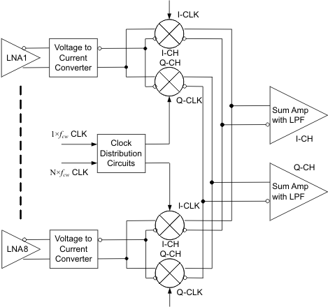 Figure 63. Simplified Block Diagram of CW Path
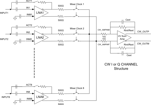
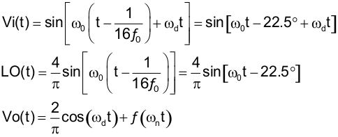
The CW mixer in the AFE5808A device is passive and switch based; passive mixer adds less noise than active mixers. The CW mixer achieves good performance at low power. Figure 65 and Equation 1 describe the principles of mixer operation, where Vi(t), Vo(t), and LO(t) are input, output and local oscillator (LO) signals for a mixer respectively. The LO(t) is square-wave based and includes odd harmonic components as shown in Equation 1.
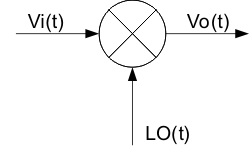 Figure 65. Block Diagram of Mixer Operation
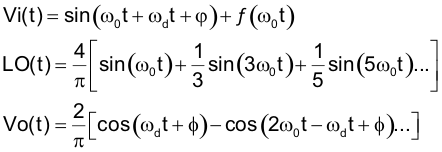
From Equation 1, the 3rd and 5th order harmonics from the LO can interface with the 3rd and 5th order harmonic signals in the Vi(t); or the noise around the 3rd and 5th order harmonics in the Vi(t). Therefore, the mixer’s performance is degraded. To eliminate this side effect due to the square-wave demodulation, a proprietary harmonic suppression circuit is implemented in the AFE5808A device. The 3rd and 5th harmonic components from the LO can be suppressed by over 12 dB. Thus the LNA output noise around the 3rd and 5th order harmonic bands will not be down-converted to base band. Hence, better noise figure is achieved. The conversion loss of the mixer is about –4 dB, which is derived from 
The mixed current outputs of the 8 channels are summed together internally. An internal low-noise operational amplifier is used to convert the summed current to a voltage output. The internal summing amplifier is designed to accomplish low power consumption, low noise, and ease-of-use. CW outputs from multiple AFE5808A devices can be further combined on system board to implement a CW beamformer with more than 8 channels. More detailed information can be found in Application and Implementation.
Multiple clock options are supported in the AFE5808A CW path. Two CW clock inputs are required: N × ƒcw clock and 1 × ƒcw clock, where ƒcw is the CW transmitting frequency and N could be 16, 8, 4, or 1. Users have the flexibility to select the most convenient system clock solution for the AFE5808A device. In the 16 × ƒcw and 8 × ƒcw modes, the 3rd and 5th harmonic suppression feature can be supported. Thus the 16 × ƒcw and 8 × ƒcw modes achieve better performance than the 4 × ƒcw and 1 × ƒcw modes.
8.3.5.1 16 × ƒcw Mode
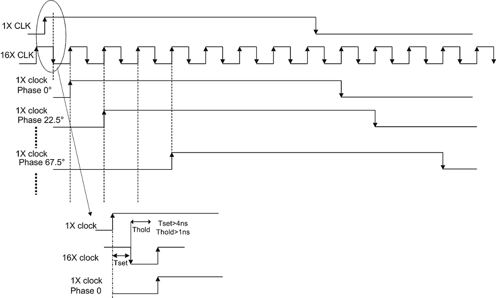
The 16 × ƒcw mode achieves the best phase accuracy compared to other modes. The 16 × ƒcw mode is the default mode for CW operation. In this mode, 16 × ƒcw and 1 × ƒcw clocks are required. 16׃cw generates LO signals with 16 accurate phases. Multiple AFE5808A devices can be synchronized by the 1 × ƒcw; that is, LO signals in multiple AFEs can have the same starting phase. The phase noise specification is critical only for the 16X clock. The 1X clock is for synchronization only, and it doesn’t require low phase noise. See the CW Clock Selection.
The top level clock distribution diagram is shown in Figure 66. Each mixer's clock is distributed through a 16 × 8 cross-point switch. The inputs of the cross-point switch are 16 different phases of the 1x clock. TI recommends aligning the rising edges of the 1 × ƒcw and 16 × ƒcw clocks.
The cross-point switch distributes the clocks with appropriate phase delay to each mixer. For example, Vi(t) is a received signal with a delay of  , a delayed LO(t) should be applied to the mixer to compensate for the
  delay. Thus a 22.5⁰ delayed clock, that is
  , is selected for this channel. The mathematic calculation is expressed in Equation 2.
Vo(t) represents the demodulated Doppler signal of each channel. When the doppler signals from N channels are summed, the signal-to-noise ratio improves.
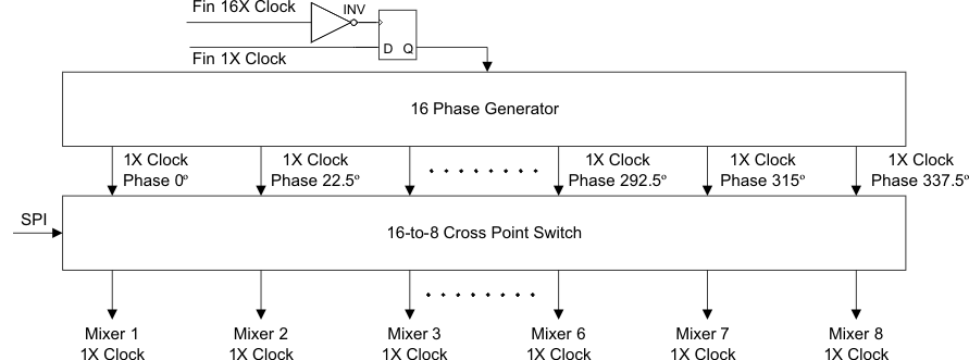 Figure 66. CW Mixer Clock Generation
8.3.5.2 8 × ƒcw and 4 × ƒcw Modes
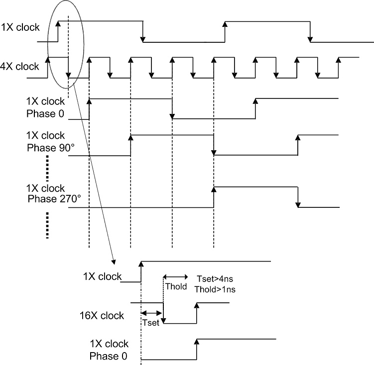
8 × ƒcw and 4 × ƒcw modes are alternative modes when higher frequency clock solution (that is 16 × ƒcw clock) is not available in system. Figure 68 shows the block diagram of these two modes.
Good phase accuracy and matching are also maintained. Quadature clock generator is used to create in-phase and quadrature clocks with exactly 90° phase difference. The only difference between 8 × ƒcw and 4 × ƒcw modes is the accessibility of the 3rd and 5th harmonic suppression filter. In the 8 × ƒcw mode, the suppression filter can be supported. In both modes,  phase delay resolution is achieved by weighting the in-phase and quadrature paths correspondingly. For example, if a delay of
  or 22.5° is targeted, the weighting coefficients should follow Equation 3, assuming Iin and Qin are sin(ω0t) and cos(ω0t) respectively:
Therefore, after I/Q mixers, phase delay in the received signals is compensated. The mixers’ outputs from all channels are aligned and added linearly to improve the signal-to-noise ratio. TI recommends having the 4 × ƒcw or 8 × ƒcw and 1 × ƒcw clocks aligned both at the rising edge.
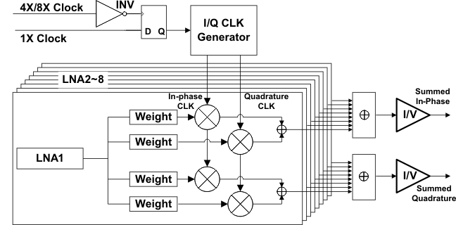 Figure 68. 8 X ƒcw and 4 X ƒcw Block Diagram
8.3.5.3 1 × ƒcw Mode
The 1x ƒcw mode requires in-phase and quadrature clocks with low phase noise specifications. The  phase delay resolution is also achieved by weighting the in-phase and quadrature signals as described in the 8 × ƒcw and 4 × ƒcw modes.
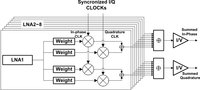 Figure 70. Block Diagram of 1 x ƒcw mode
8.3.6 Equivalent Circuits
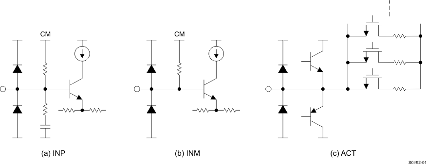 Figure 71. Equivalent Circuits of LNA inputs
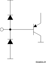 Figure 72. Equivalent Circuits of VCNTLP/M
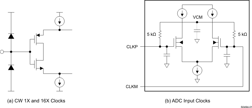 Figure 73. Equivalent Circuits of Clock Inputs
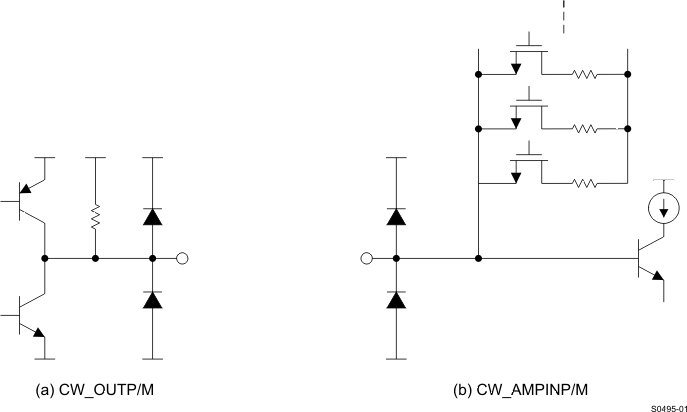 Figure 74. Equivalent Circuits of CW Summing Amplifier Inputs and Outputs
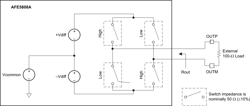 Figure 75. Equivalent Circuits of LVDS Outputs
8.3.7 LVDS Output Interface Description
The AFE5808A device has a LVDS output interface that supports multiple output formats. The ADC resolutions can be configured as 12 bit or 14 bit as shown in the LVDS timing diagrams Figure 1. The ADCs in the AFE5808A are running at 14 bit; 2 LSBs are removed when 12-bit output is selected; and two 0s are added at LSBs when 16-bit output is selected. Appropriate ADC resolutions can be selected for optimizing system performance-cost effectiveness. When the devices run at 16-bit mode, higher end FPGAs are required to process a higher rate of LVDS data. Corresponding register settings are shown in Table 5.
8.4 Device Functional Modes
The AFE5808A device is a highly-integrated AFE solution. The AFE5808A device has two functional modes: pulsed-wave imaging mode and continous-wave Doppler imaging mode. When the AFE5808A device operates in the pulsed-wave imaging mode, LNA, VCAT, PGA, LPF, and 14-bit ADC are active. In the CWD imaging mode, only LNA and CW mixer are enabled. Either mode can be enabled or programmed by the registers described in the following sections.
8.4.1 TGC Mode
By default, after reset the AFE is configured in TGC mode. Depending upon the system requirements, the device can be programmed in a suitable power mode using the register bits shown in Table 6. In the TGC mode, the digital demodulator after ADC can be enabled as well for further digital processing.
8.4.2 CW Mode
To configure the device in CW mode, set the CW_TGC_SEL (0x36[8]) register bit to 1. To save power, the voltage-controlled attenuator and programmable gain amplifier in the TGC path can be disabled by setting the 0x35[12] to 1. Also, the ADC can be powered down completely using the 0x1[0] . Usually only half the number of channels in a system are active in the CW mode. Thus, the individual channel control can power down unused channels and save power; see register 0x1[9:2] and 0x35[7:0].
8.4.3 TGC + CW Mode
In systems that require fast switching between the TGC and CW modes, either mode can be selected simply by setting the CW_TGC_SEL register bit.
8.4.4 Test Modes
The AFE5808A device includes multiple test modes to accelerate system development.
8.4.4.1 ADC Test Modes
The AFE5808A device can output a variety of test patterns on the LVDS outputs. These test patterns replace the normal ADC data output. The device may also be made to output 6 preset patterns:
- Ramp: Setting Register 2[15:13] = 111 causes all the channels to output a repeating full-scale ramp pattern. The ramp increments from zero code to full-scale code in steps of 1 LSB every clock cycle. After hitting the full-scale code, the ADC output returns back to zero code and ramps again.
- Zeros: The device can be programmed to output all 0s by setting Register 2[15:13] = 110.
- Ones: The device can be programmed to output all 1s by setting Register 2[15:13] = 100.
- Deskew Pattern: When 2[15:13] = 010; this mode replaces the 14-bit ADC output with the 01010101010101 word.
- Sync Pattern: When 2[15:13] = 001, the normal ADC output is replaced by a fixed 11111110000000 word.
- Toggle: When 2[15:13] = 101, the normal ADC output is alternating between 1s and 0s. The start state of ADC word can be either 1s or 0s.
- Custom Pattern: This mode can be enabled when 2[15:13] = 011. Users can write the required VALUE into register bits <CUSTOM PATTERN>, which is Register 5[13:0]. Then, the device will output VALUE at its outputs, about 3 to 4 ADC clock cycles after the 24th rising edge of SCLK. So, the time taken to write one value is 24 SCLK clock cycles + 4 ADC clock cycles. To change the customer pattern value, users can repeat writing Register 5[13:0] with a new value. Due to the speed limit of SPI, the refresh rate of the custom pattern may not be high. For example, 128 points custom pattern takes approximately 128 × (24 SCLK clock cycles + 4 ADC clock cycles).
NOTE
Only one of the above ADC patterns can be active at any given instant.
8.4.4.2 VCA Test Mode
The VCA has a test mode in which the CH7 and CH8 PGA outputs can be brought to the CW pins. By monitoring these PGA outputs, the functionality of VCA operation can be verified. The PGA outputs are connected to the virtual ground pins of the summing amplifier (CW_IP_AMPINM/P, CW_QP_AMPINM/P) through 5-kΩ resistors. The PGA outputs can be monitored at the summing amplifier outputs when the LPF capacitors CEXT are removed. The signals at the summing amplifier outputs are attenuated due to the 5-kΩ resistors. The attenuation coefficient is RINT/EXT / 5 kΩ.
If users would like to check the PGA outputs without removing CEXT, an alternative way is to measure the PGA outputs directly at the CW_IP_AMPINM/P and CW_QP_AMPINM/P when the CW summing amplifier is powered down.
Some registers are related to this test mode, PGA Test Mode Enable: Reg59[9]; Buffer Amplifier Power Down Reg59[8]; and Buffer Amplifier Gain Control Reg54[4:0]. Based on the buffer amplifier configuration, the registers can be set in different ways:
-
Configuration 1
- In this configuration, the test outputs can be monitored at CW_AMPINP/M.
- Reg59[9] = 1; test mode enabled
- Reg59[8] = 0; buffer amplifier powered-down
-
Configuration 2
- In this configuration, the test outputs can be monitored at CW_OUTP/M.
- Reg59[9] = 1; test mode enabled
- Reg59[8] = 1; buffer amplifier powered on
- Reg54[4:0] = 10H; internal feedback 2-kΩ resistor enabled. Different values can be used as well.
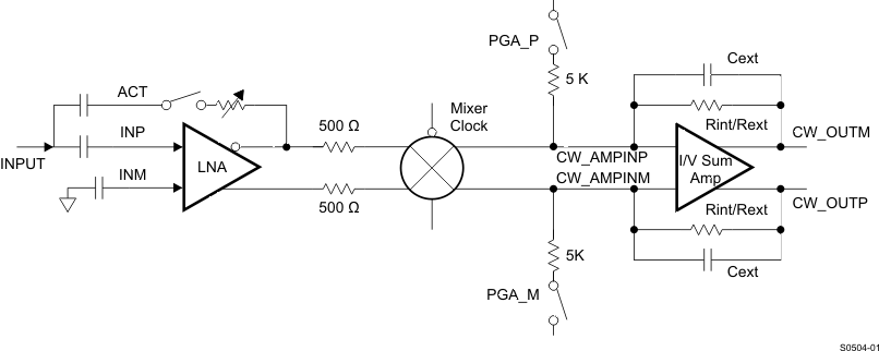 Figure 76. AFE5808A PGA Test Mode
8.4.5 Power Management
8.4.5.1 Power and Performance Optimization
The AFE5808A device has options to adjust power consumption and meet different noise performances. This feature would be useful for portable systems operated by batteries when low power is more desired. See Electrical Characteristics as well as the Typical Characteristics for more information.
8.4.5.2 Power Management Priority
Power management plays a critical role to extend battery life and ensure long operation time. The AFE5808A device has fast and flexible power-down and power-up control, which can maximize battery life. The AFE5808A device can be powered down and powered up through external pins or internal registers. The following table indicates the affected circuit blocks and priorities when the power management is invoked. The higher priority controls can overwrite the lower priority ones. In the device, all the power down controls are logically ORed to generate final power down for different blocks. Thus, the higher priority controls can cover the lower priority ones. The AFE5808A register settings are maintained when the AFE5808A is in either partial power down mode or complete power down mode.
Table 2. Power Management Priority
| PIN OR REGISTER | NAME | BLOCKS | PRIORITY |
|---|---|---|---|
| Pin | PDN_GLOBAL | All | High |
| Pin | PDN_VCA | LNA + VCAT+ PGA | Medium |
| Register | VCA_PARTIAL_PDN | LNA + VCAT+ PGA | Low |
| Register | VCA_COMPLETE_PDN | LNA + VCAT+ PGA | Medium |
| Pin | PDN_ADC | ADC | Medium |
| Register | ADC_PARTIAL_PDN | ADC | Low |
| Register | ADC_COMPLETE_PDN | ADC | Medium |
| Register | PDN_VCAT_PGA | VCAT + PGA | Lowest |
| Register | PDN_LNA | LNA | Lowest |
8.4.5.3 Partial Power Up and Power Down Mode
The partial power-up and power-down mode is also called as fast power-up and power-down mode. In this mode, most amplifiers in the signal path are powered down, while the internal reference circuits remain active as well as the LVDS clock circuit (that is the LVDS circuit still generates its frame and bit clocks).
The partial power down function allows the AFE5808A device to wake up from a low-power state quickly. This configuration ensures that the external capacitors are discharged slowly; thus, a minimum wake-up time is needed as long as the charges on those capacitors are restored. The VCA wake-up response is typically about 2 μs or 1% of the power down duration whichever is larger. The longest wake-up time depends on the capacitors connected at INP and INM, as the wake-up time is the time required to recharge the caps to the desired operating voltages. For 0.1 μF at INP and 15 nF at INM can give a wake-up time of 2.5 ms. For larger capacitors this time will be longer. The ADC wake-up time is about 1 μs. Thus the AFE5808A wake-up time is more dependent on the VCA wake-up time. This also assumes that the ADC clock has been running for at least 50 µs before normal operating mode resumes. The power-down time is instantaneous, less than 1 µs.
This fast wake-up response is desired for portable ultrasound applications in which the power saving is critical. The pulse repetition frequency of a ultrasound system could vary from 50 KHz to 500 Hz, while the imaging depth (that is, the active period for a receive path) varies from 10 μs to hundreds of µs. The power saving can be pretty significant when a system’s PRF is low. In some cases, only the VCA would be powered down while the ADC keeps running normally to ensure minimal impact to FPGAs.
In the partial power-down mode, the AFE5808A typically dissipates only 26 mW/ch, representing an 80% power reduction compared to the normal operating mode. This mode can be set using either pins (PDN_VCA and PDN_ADC) or register bits (VCA_PARTIAL_PDN and ADC_PARTIAL_PDN).
8.4.5.4 Complete Power-Down Mode
To achieve the lowest power dissipation of 0.7 mW/CH, the AFE5808A device can be placed into a complete power-down mode. This mode is controlled through the registers ADC_COMPLETE_PDN, VCA_COMPLETE_PDN or PDN_GLOBAL pin. In the complete power-down mode, all circuits including reference circuits within the AFE5808A device are powered down; and the capacitors connected to the AFE5808A device are discharged. The wake-up time depends on the time needed to recharge these capacitors. The wake-up time depends on the time that the AFE5808A device spends in shutdown mode. 0.1 μF at INP and 15 nF at INM can give a wake-up time close to 2.5 ms.
8.4.5.5 Power Saving in CW Mode
Usually only half the number of channels in a system are active in the CW mode. Thus the individual channel control through ADC_PDN_CH <7:0> and VCA_PDN_CH <7:0> can power down unused channels and save power consumption greatly. Under the default register setting in the CW mode, the voltage controlled attenuator, PGA, and ADC are still active. During the debug phase, both the PW and CW paths can be running simultaneously. In real operation, these blocks need to be powered down manually.
8.5 Programming
8.5.1 Serial Register Timing
8.5.1.1 Serial Register Write Description
Programming of different modes can be done through the serial interface formed by pins SEN (serial interface enable), SCLK (serial interface clock), SDATA (serial interface data) and RESET. All these pins have a pulldown resistor to GND of 20 kΩ. Serial shift of bits into the device is enabled when SEN is low. Serial data SDATA is latched at every rising edge of SCLK when SEN is active (low). The serial data is loaded into the register at every 24th SCLK rising edge when SEN is low. If the word length exceeds a multiple of 24 bits, the excess bits are ignored. Data can be loaded in multiple of 24-bit words within a single active SEN pulse (there is an internal counter that counts groups of 24 clocks after the falling edge of SEN). The interface can work with the SCLK frequency from 20 MHz down to low speeds (a few Hz) and even with non-50% duty cycle SCLK. The data is divided into two main portions: a register address (8 bits) and the data itself (16 bits) to load on the addressed register. When writing to a register with unused bits, these must be set to 0. Figure 77 shows this process.
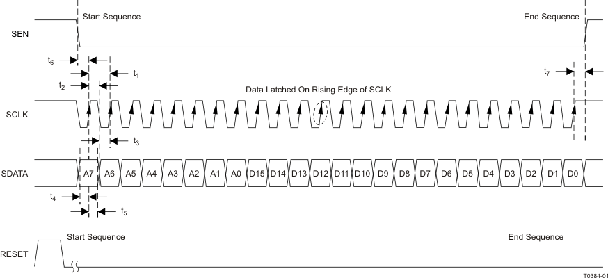 Figure 77. SPI Timing
8.5.1.2 Register Readout Description
The device includes an option where the contents of the internal registers can be read back. This may be useful as a diagnostic test to verify the serial interface communication between the external controller and the AFE. First, the <REGISTER READOUT ENABLE> bit (Reg0[1]) needs to be set to '1', then the user should initiate a serial interface cycle specifying the address of the register (A7 to A0) whose content has to be read. The data bits are don’t care. The device will output the contents (D15-D0) of the selected register on the SDOUT pin. SDOUT has a typical delay t8 of 20 ns from the falling edge of the SCLK. For lower speed SCLK, SDOUT can be latched on the rising edge of SCLK. For higher speed SCLK, for example, the SCLK period lesser than 60 ns, TI recommends latching the SDOUT at the next falling edge of SCLK. Figure 78 shows this operation (the time specifications follow the same information provided. In the readout mode, users still can access the <REGISTER READOUT ENABLE> through SDATA/SCLK/SEN. To enable serial register writes, set the <REGISTER READOUT ENABLE> bit back to '0'.
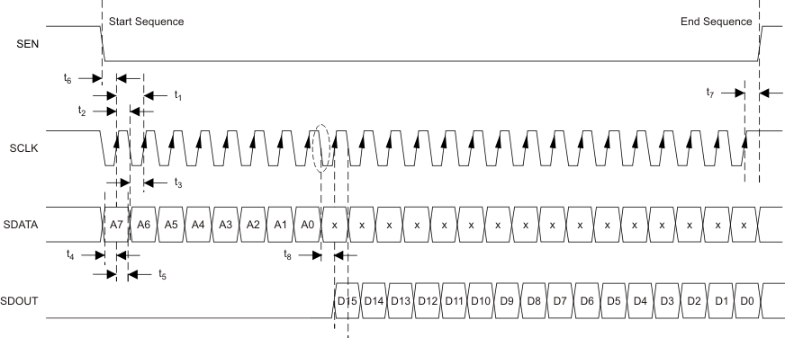 Figure 78. Serial Interface Register Read
The AFE5808A SDOUT buffer is tri-stated and will get enabled only when 0[1] (REGISTER READOUT ENABLE) is enabled. SDOUT pins from multiple AFE5808As can be tied together without any pullup resistors. Level shifter SN74AUP1T04 can be used to convert 1.8-V logic to 2.5-V/3.3-V logics if needed.
8.6 Register Maps
A reset process is required at the AFE5808A initialization stage. Initialization can be done in one of two ways:
- Through a hardware reset by applying a positive pulse in the RESET pin
- Through a software reset using the serial interface by setting the SOFTWARE RESET bit to high. Setting this bit initializes the internal registers to the respective default values (all zeros) and then self-resets the SOFTWARE RESET bit to low. In this case, the RESET pin can stay low (inactive).
After reset, all ADC and VCA registers are set to ‘0’, that is default settings. During register programming, all reserved/unlisted register bits need to be set as ‘0’. Register settings are maintained when the AFE5808A device is in either partial power down mode or complete power down mode.
8.6.1 ADC Register Map
Table 3. ADC Register Map
| ADDRESS (DEC) |
ADDRESS (HEX) |
DEFAULT VALUE |
FUNCTION | DESCRIPTION |
|---|---|---|---|---|
| 0[0] | 0x0[0] | 0 | SOFTWARE_RESET | 0: Normal operation; 1: Resets the device and self-clears the bit to '0' |
| 0[1] | 0x0[1] | 0 | REGISTER_READOUT_ENABLE | 0:Disables readout; 1: enables readout of register at SDOUT Pin |
| 1[0] | 0x1[0] | 0 | ADC_COMPLETE_PDN | 0: Normal 1: Complete Power down |
| 1[1] | 0x1[1] | 0 | LVDS_OUTPUT_DISABLE | 0: Output Enabled; 1: Output disabled |
| 1[9:2] | 0x1[9:2] | 0 | ADC_PDN_CH<7:0> | 0: Normal operation; 1: Power down. Power down Individual ADC channels. 1[9]→CH8…1[2]→CH1 |
| 1[10] | 0x1[10] | 0 | PARTIAL_PDN | 0: Normal Operation; 1: Partial Power Down ADC |
| 1[11] | 0x1[11] | 0 | LOW_FREQUENCY_ NOISE_SUPPRESSION |
0: No suppression; 1: Suppression Enabled |
| 1[13] | 0x1[13] | 0 | EXT_REF | 0: Internal Reference; 1: External Reference. VREF_IN is used. Both 3[15] and 1[13] should be set as 1 in the external reference mode |
| 1[14] | 0x1[14] | 0 | LVDS_OUTPUT_RATE_2X | 0: 1x rate; 1: 2x rate. Combines data from 2 channels on 1 LVDS pair. When ADC clock rate is low, this feature can be used |
| 1[15] | 0x1[15] | 0 | SINGLE-ENDED_CLK_MODE | 0: Differential clock input; 1: Single-ended clock input |
| 2[2:0] | 0x2[2:0] | 0 | RESERVED | Set to 0 |
| 2[10:3] | 0x2[10:3] | 0 | POWER-DOWN_LVDS | 0: Normal operation; 1: PDN Individual LVDS outputs. 2[10]→CH8…2[3]→CH1 |
| 2[11] | 0x2[11] | 0 | AVERAGING_ENABLE | 0: No averaging; 1: Average 2 channels to increase SNR |
| 2[12] | 0x2[12] | 0 | LOW_LATENCY | 0: Default Latency with digital features supported, 11 cycle latency 1: Low Latency with digital features bypassed, 8 cycle latency |
| 2[15:13] | 0x2[15:13] | 0 | TEST_PATTERN_MODES | 000: Normal operation; 001: Sync; 010: De-skew; 011: Custom; 100:All 1's; 101: Toggle; 110: All 0's; 111: Ramp |
| 3[7:0] | 0x3[7:0] | 0 | INVERT_CHANNELS | 0: No inverting; 1:Invert channel digital output. 3[7]→CH8;3[0]→CH1 |
| 3[8] | 0x3[8] | 0 | CHANNEL_OFFSET_ SUBSTRACTION_ENABLE | 0: No offset subtraction; 1: Offset value Subtract Enabled |
| 3[9:11] | 0x3[9:11] | 0 | RESERVED | Set to 0 |
| 3[12] | 0x3[12] | 0 | DIGITAL_GAIN_ENABLE | 0: No digital gain; 1: Digital gain Enabled |
| 3[14:13] | 0x3[14:13] | 0 | SERIALIZED_DATA_RATE | Serialization factor 00: 14x 01: 16x 10: reserved 11: 12x when 4[1] = 1. In the 16x serialization rate, two 0s are filled at two LSBs (see Table 5) |
| 3[15] | 0x3[15] | 0 | ENABLE_EXTERNAL_ REFERENCE_MODE |
0: Internal reference mode; 1: Set to external reference mode Note: both 3[15] and 1[13] should be set as 1 when configuring the device in the external reference mode |
| 4[1] | 0x4[1] | 0 | ADC_RESOLUTION_SELECT | 0: 14bit; 1: 12bit |
| 4[3] | 0x4[3] | 0 | ADC_OUTPUT_FORMAT | 0: 2's complement; 1: Offset binary |
| 4[4] | 0x4[4] | 0 | LSB_MSB_FIRST | 0: LSB first; 1: MSB first |
| 5[13:0] | 0x5[13:0] | 0 | CUSTOM_PATTERN | Custom pattern data for LVDS output (2[15:13] = 011) |
| 10[8] | 0xA[8] | 0 | SYNC_PATTERN | 0: Test pattern outputs of 8 channels are NOT synchronized. 1: Test pattern outputs of 8 channels are synchronized. |
| 13[9:0] | 0xD[9:0] | 0 | OFFSET_CH1 | Value to be subtracted from channel 1 code |
| 13[15:11] | 0xD[15:11] | 0 | DIGITAL_GAIN_CH1 | 0 to 6 dB in 0.2-dB steps |
| 15[9:0] | 0xF[9:0] | 0 | OFFSET_CH2 | value to be subtracted from channel 2 code |
| 15[15:11] | 0xF[15:11] | 0 | DIGITAL_GAIN_CH2 | 0 to 6dB in 0.2-dB steps |
| 17[9:0] | 0x11[9:0] | 0 | OFFSET_CH3 | value to be subtracted from channel 3 code |
| 17[15:11] | 0x11[15:11] | 0 | DIGITAL_GAIN_CH3 | 0 to 6 dB in 0.2-dB steps |
| 19[9:0] | 0x13[9:0] | 0 | OFFSET_CH4 | value to be subtracted from channel 4 code |
| 19[15:11] | 0x13[15:11] | 0 | DIGITAL_GAIN_CH4 | 0 to 6 dB in 0.2-dB steps |
| 21[0] | 0x15[0] | 0 | DIGITAL_HPF_FILTER_ENABLE_ CH1-4 | 0: Disable the digital HPF filter; 1: Enable for 1-4 channels |
| 21[4:1] | 0x15[4:1] | 0 | DIGITAL_HPF_FILTER_K_CH1-4 | Set K for the high-pass filter (k from 2 to 10, that is 0010B to 1010B). This group of four registers controls the characteristics of a digital high-pass transfer function applied to the output data, following the formula: y(n) = 2k / (2k + 1) [x(n) – x(n – 1) + y(n – 1)] (see Table 4 and Figure 58) |
| 25[9:0] | 0x19[9:0] | 0 | OFFSET_CH8 | value to be subtracted from channel 8 code |
| 25[15:11] | 0x19[15:11] | 0 | DIGITAL_GAIN_CH8 | 0 to 6 dB in 0.2-dB steps |
| 27[9:0] | 0x1B[9:0] | 0 | OFFSET_CH7 | value to be subtracted from channel 7 code |
| 27[15:11] | 0x1B[15:11] | 0 | DIGITAL_GAIN_CH7 | 0 to 6dB in 0.2-dB steps |
| 29[9:0] | 0x1D[9:0] | 0 | OFFSET_CH6 | value to be subtracted from channel 6 code |
| 29[15:11] | 0x1D[15:11] | 0 | DIGITAL_GAIN_CH6 | 0 to 6 dB in 0.2-dB steps |
| 31[9:0] | 0x1F[9:0] | 0 | OFFSET_CH5 | value to be subtracted from channel 5 code |
| 31[15:11] | 0x1F[15:11] | 0 | DIGITAL_GAIN_CH5 | 0 to 6 dB in 0.2-dB steps |
| 33[0] | 0x21[0] | 0 | DIGITAL_HPF_FILTER_ENABLE_ CH5-8 | 0: Disable the digital HPF filter; 1: Enable for 5-8 channels |
| 33[4:1] | 0x21[4:1] | 0 | DIGITAL_HPF_FILTER_K_CH5-8 | Set K for the high-pass filter (k from 2 to 10, 010B to 1010B) This group of four registers controls the characteristics of a digital high-pass transfer function applied to the output data, following the formula: y(n) = 2k / (2k + 1) [x(n) – x(n – 1) + y(n – 1)] (see Table 4 and Figure 58) |
| 66[15] | 0x42[15] | 0 | DITHER | 0: Disable dither function. 1: Enable dither function. Improve the ADC linearity with slight noise degradation. |
8.6.2 ADC Register/Digital Processing Description
The ADC in the AFE5808A device has extensive digital processing functionalities that can be used to enhance ultrasound system performance. The digital processing blocks are arranged as in Figure 79.
 Figure 79. ADC Digital Block Diagram
8.6.2.1 AVERAGING_ENABLE: Address: 2[11]
When set to 1, two samples, corresponding to two consecutive channels, are averaged (channel 1 with 2, 3 with 4, 5 with 6, and 7 with 8). If both channels receive the same input, the net effect is an improvement in SNR. The averaging is performed as:
- Channel 1 + channel 2 comes out on channel 3
- Channel 3 + channel 4 comes out on channel 4
- Channel 5 + channel 6 comes out on channel 5
- Channel 7 + channel 8 comes out on channel 6
8.6.2.2 ADC_OUTPUT_FORMAT: Address: 4[3]
The ADC output, by default, is in 2’s-complement mode. Programming the ADC_OUTPUT_FORMAT bit to 1 inverts the MSB, and the output becomes straight-offset binary mode.
8.6.2.3 DIGITAL_GAIN_ENABLE: Address: 3[12]
Setting this bit to 1 applies to each channel i the corresponding gain given by DIGTAL_GAIN_CHi <15:11>. The gain is given as 0dB + 0.2dB × DIGTAL_GAIN_CHi<15:11>. For instance, if DIGTAL_GAIN_CH5<15:11> = 3, channel 5 is increased by 0.6dB gain. DIGTAL_GAIN_CHi <15:11> = 31 produces the same effect as DIGTAL_GAIN_CHi <15:11> = 30, setting the gain of channel i to 6dB.
8.6.2.4 DIGITAL_HPF_ENABLE
- CH1-4: Address 21[0]
- CH5-8: Address 33[0]
8.6.2.5 DIGITAL_HPF_FILTER_K_CHX
- CH1-4: Address 21[4:1]
- CH5-8: Address 3[4:1]
This group of registers controls the characteristics of a digital high-pass transfer function applied to the output data, following Equation 4.

These digital HPF registers (one for the first four channels and one for the second group of four channels) describe the setting of K. The digital high pass filter can be used to suppress low frequency noise which commonly exists in ultrasound echo signals. The digital filter can significantly benefit near field recovery time due to T/R switch low frequency response. Table 4 shows the cut-off frequency vs K, also see Figure 58.
Table 4. Digital HPF –1-dB Corner Frequency vs K and Fs
| k | 40 MSPS | 50 MSPS | 65 MSPS |
|---|---|---|---|
| 2 | 2780 kHz | 3480 kHz | 4520 kHz |
| 3 | 1490 kHz | 1860 kHz | 2420 kHz |
| 4 | 770 kHz | 960 kHz | 1250 kHz |
8.6.2.6 LOW_FREQUENCY_NOISE_SUPPRESSION: Address: 1[11]
The low-frequency noise suppression mode is especially useful in applications where good noise performance is desired in the frequency band of 0 MHz to 1 MHz (around DC). Setting this mode shifts the low-frequency noise of the AFE5808A device to approximately Fs / 2, thereby moving the noise floor around DC to a much lower value. Register bit 1[11] is used for enabling or disabling this feature. When this feature is enabled, power consumption of the device increases by approximately 1 mW/CH.
8.6.2.7 LVDS_OUTPUT_RATE_2X: Address: 1[14]
The output data always uses a DDR format, with valid/different bits on the positive as well as the negative edges of the LVDS bit clock, DCLK. The output rate is set by default to 1X (LVDS_OUTPUT_RATE_2X = 0), where each ADC has one LVDS stream associated with it. If the sampling rate is low enough, two ADCs can share one LVDS stream, thereby lowering the power consumption devoted to the interface. The unused outputs will output zero. To avoid consumption from those outputs, no termination must not be connected to them. The distribution on the used output pairs is done in the following way:
- Channel 1 and channel 2 come out on channel 3. Channel 1 comes out first.
- Channel 3 and channel 4 come out on channel 4. Channel 3 comes out first.
- Channel 5 and channel 6 come out on channel 5. Channel 5 comes out first.
- Channel 7 and channel 8 come out on channel 6. Channel 7 comes out first.
8.6.2.8 CHANNEL_OFFSET_SUBSTRACTION_ENABLE: Address: 3[8]
Setting this bit to 1 enables the subtraction of the value on the corresponding OFFSET_CHx<9:0> (offset for channel i) from the ADC output. The number is specified in 2s-complement format. For example, OFFSET_CHx<9:0> = 11 1000 0000 means subtract 128. For OFFSET_CHx<9:0> = 00 0111 1111 the effect is to subtract 127. In effect, both addition and subtraction can be performed. Note that the offset is applied before the digital gain (see ADC_OUTPUT_FORMAT: Address: 4[3]). The whole data path is 2s-complement throughout internally, with digital gain being the last step. Only when ADC_OUTPUT_FORMAT = 1 (straight binary output format) is the 2s-complement word translated into offset binary at the end.
8.6.2.9 SERIALIZED_DATA_RATE: Address: 3[14:13]
Table 5. Corresponding Register Settings
| LVDS Rate | 12 bit (6X DCLK) | 14 bit (7X DCLK) | 16 bit (8X DCLK) |
|---|---|---|---|
| Reg 3 [14:13] | 11 | 00 | 01 |
| Reg 4 [2:0] | 010 | 000 | 000 |
| Description | 2 LSBs removed | N/A | 2 0s added at LSBs |
8.6.2.10 TEST_PATTERN_MODES: Address: 2[15:13]
The AFE5808A device can output a variety of test patterns on the LVDS outputs. These test patterns replace the normal ADC data output. The device may also be made to output 6 preset patterns:
- Ramp: Setting Register 2[15:13] = 111 causes all the channels to output a repeating full-scale ramp pattern. The ramp increments from zero code to full-scale code in steps of 1 LSB every clock cycle. After hitting the full-scale code, it returns back to zero code and ramps again.
- Zeros: The device can be programmed to output all zeros by setting Register 2[15:13] = 110;
- Ones: The device can be programmed to output all 1s by setting Register 2[15:13] = 100;
- Deskew Patten: When 2[15:13] = 010; this mode replaces the 14-bit ADC output with the 01010101010101 word.
- Sync Pattern: When 2[15:13] = 001, the normal ADC output is replaced by a fixed 11111110000000 word.
- Toggle: When 2[15:13] = 101, the normal ADC output is alternating between 1's and 0's. The start state of ADC word can be either 1's or 0's.
- Custom Pattern: It can be enabled when 2[15:13] = 011;. Users can write the required VALUE into register bits <CUSTOM PATTERN> which is Register 5[13:0]. Then the device will output VALUE at its outputs, about 3 to 4 ADC clock cycles after the 24th rising edge of SCLK. So, the time taken to write one value is 24 SCLK clock cycles + 4 ADC clock cycles. To change the customer pattern value, users can repeat writing Register 5[13:0] with a new value. Due to the speed limit of SPI, the refresh rate of the custom pattern may not be high. For example, 128 points custom pattern will take approximately 128 × (24 SCLK clock cycles + 4 ADC clock cycles).
NOTE
Only one of the above patterns can be active at any given instant.
8.6.2.11 SYNC_PATTERN: Address: 10[8]
By enabling this bit, all channels' test pattern outputs are synchronized. When 10[8] is set as 1, the ramp patterns of all 8 channels start simultaneously.
8.6.3 VCA Register Map
Table 6. VCA Register Map
| ADDRESS (DEC) |
ADDRESS (HEX) |
DEFAULT VALUE |
FUNCTION | DESCRIPTION |
|---|---|---|---|---|
| 50[10] | 0x32[10] | 0 | PGA_CLAMP_-6dB | 0: No clamp enabled. 1: The PGA output linearity will be degraded when PGA output signal is higher than –6 dBFS, 1 VPP. The PGA output is limited to about 1.6 VPP. ADC is not overloaded while its dynamic range is reduced by 2 dB. This setting will reduce the channel gain by about 1.5 dB. Note: 0x33[7:5] needs to be set as 000 in the low noise mode or 100 in the low/medium power mode. |
| 51[0] | 0x33[0] | 0 | RESERVED | 0 |
| 51[3:1] | 0x33[3:1] | 0 | LPF_PROGRAMMABILITY | 000: 15 MHz, 010: 20 MHz, 011: 30 MHz, 100: 10 MHz |
| 51[4] | 0x33[4] | 0 | PGA_INTEGRATOR_DISABLE (PGA_HPF_DISABLE) | 0: Enable 1: Disables offset integrator for PGA. See explanation for the PGA integrator function in Application and Implementation section |
| 51[7:5] | 0x33[7:5] | 0 | PGA_CLAMP_LEVEL | Low Noise mode: 53[11:10] = 00 000: –2 dBFS 010: 0 dBFS 1XX: Clamp is disabled Low power/Medium Power mode; 53[11:10] = 01/10 100: –2 dBFS 110: 0 dBFS 0XX: clamp is disabled Note: 0x32[10] needs to be set as 0. Note: the clamp circuit makes sure that PGA output is in linear range. For example, at 000 setting, PGA output HD3 will be worsen by 3 dB at –2 dBFS ADC input. In normal operation, clamp function can be set as 000 in the low noise mode. The maximum PGA output level can exceed 2 VPP with the clamp circuit enabled. In the low power and medium power modes, PGA_CLAMP is disabled for saving power if 51[7] = 0. |
| 51[13] | 0x33[13] | 0 | PGA_GAIN_CONTROL | 0:24 dB; 1:30 dB. |
| 52[4:0] | 0x34[4:0] | 0 | ACTIVE_TERMINATION_ INDIVIDUAL_RESISTOR_CNTL | See Table 8 Reg 52[5] should be set as '1' to access these bits |
| 52[5] | 0x34[5] | 0 | ACTIVE_TERMINATION_ INDIVIDUAL_RESISTOR_ENABLE | 0: Disables; 1: Enables internal active termination individual resistor control |
| 52[7:6] | 0x34[7:6] | 0 | PRESET_ACTIVE_ TERMINATIONS | 00: 50 Ω, 01: 100 Ω, 10: 200 Ω, 11: 400 Ω. (Note: the device will adjust resistor mapping (52[4:0]) automatically. 50-Ω active termination is NOT supported in 12 dB LNA setting. Instead, '00' represents high impedance mode when LNA gain is 12 dB) |
| 52[8] | 0x34[8] | 0 | ACTIVE TERMINATION ENABLE | 0: Disables; 1: Enables active termination |
| 52[10:9] | 0x34[10:9] | 0 | LNA_INPUT_CLAMP_SETTING | 00: Auto setting, 01: 1.5 VPP, 10: 1.15 VPP and 11: 0.6 VPP |
| 52[11] | 0x34[11] | 0 | RESERVED | Set to 0 |
| 52[12] | 0x34[12] | 0 | LNA_INTEGRATOR_DISABLE (LNA_HPF_DISABLE) |
0: Enables; 1: Disables offset integrator for LNA. See the explanation for this function in the following section |
| 52[14:13] | 0x34[14:13] | 0 | LNA_GAIN | 00: 18 dB; 01: 24 dB; 10: 12 dB; 11: Reserved |
| 52[15] | 0x34[15] | 0 | LNA_INDIVIDUAL_CH_CNTL | 0: Disable; 1: Enable LNA individual channel control. See Register 57 for details |
| 53[7:0] | 0x35[7:0] | 0 | PDN_CH<7:0> | 0: Normal operation; 1: Powers down corresponding channels. Bit7→CH8, Bit6→CH7…Bit0→CH1. PDN_CH will shut down whichever blocks are active depending on TGC mode or CW mode |
| 53[8] | 0x35[8] | 0 | RESERVED | Set to 0 |
| 53[9] | 0x35[9] | 0 | RESERVED | Set to 0 |
| 53[10] | 0x35[10] | 0 | LOW_POWER | 0: Low noise mode; 1: Sets to low power mode (53[11] = 0). At 30 dB PGA, total chain gain may slightly change. See typical characteristics |
| 53[11] | 0x35[11] | 0 | MED_POWER | 0: Low noise mode; 1: Sets to medium power mode(53[10] = 0). At 30 dB PGA, total chain gain may slightly change. See typical characteristics |
| 53[12] | 0x35[12] | 0 | PDN_VCAT_PGA | 0: Normal operation; 1: Powers down VCAT (voltage-controlled-attenuator) and PGA |
| 53[13] | 0x35[13] | 0 | PDN_LNA | 0: Normal operation; 1: Powers down LNA only |
| 53[14] | 0x35[14] | 0 | VCA_PARTIAL_PDN | 0: Normal operation; 1: Powers down LNA, VCAT, and PGA partially(fast wake response) |
| 53[15] | 0x35[15] | 0 | VCA_COMPLETE_PDN | 0: Normal operation; 1: Powers down LNA, VCAT, and PGA completely (slow wake response). This bit can overwrite 53[14]. |
| 54[4:0] | 0x36[4:0] | 0 | CW_SUM_AMP_GAIN_CNTL | Selects Feedback resistor for the CW Amplifier as per Table 8 below |
| 54[5] | 0x36[5] | 0 | CW_16X_CLK_SEL | 0: Accepts differential clock; 1: Accepts CMOS clock |
| 54[6] | 0x36[6] | 0 | CW_1X_CLK_SEL | 0: Accepts CMOS clock; 1: Accepts differential clock |
| 54[7] | 0x36[7] | 0 | RESERVED | Set to 0 |
| 54[8] | 0x36[8] | 0 | CW_TGC_SEL | 0: TGC Mode; 1 : CW Mode Note : VCAT and PGA are still working in CW mode. They should be powered down separately through 53[12] |
| 54[9] | 0x36[9] | 0 | CW_SUM_AMP_ENABLE | 0: enables CW summing amplifier; 1: disables CW summing amplifier Note: 54[9] is only effective in CW mode. |
| 54[11:10] | 0x36[11:10] | 0 | CW_CLK_MODE_SEL | 00: 16X mode; 01: 8X mode; 10: 4X mode; 11: 1X mode |
| 55[3:0] | 0x37[3:0] | 0 | CH1_CW_MIXER_PHASE | 0000→1111, 16 different phase delays, see Table 12 |
| 55[7:4] | 0x37[7:4] | 0 | CH2_CW_MIXER_PHASE | |
| 55[11:8] | 0x37[11:8] | 0 | CH3_CW_MIXER_PHASE | |
| 55[15:12] | 0x37[15:12] | 0 | CH4_CW_MIXER_PHASE | |
| 56[3:0] | 0x38[3:0] | 0 | CH5_CW_MIXER_PHASE | |
| 56[7:4] | 0x38[7:4] | 0 | CH6_CW_MIXER_PHASE | |
| 56[11:8] | 0x38[11:8] | 0 | CH7_CW_MIXER_PHASE | |
| 56[15:12] | 0x38[15:12] | 0 | CH8_CW_MIXER_PHASE | |
| 57[1:0] | 0x39[1:0] | 0 | CH1_LNA_GAIN_CNTL | 00: 18 dB; 01: 24 dB; 10: 12 dB; 11: Reserved REG52[15] should be set as '1' |
| 57[3:2] | 0x39[3:2] | 0 | CH2_LNA_GAIN_CNTL | |
| 57[5:4] | 0x39[5:4] | 0 | CH3_LNA_GAIN_CNTL | 00: 18 dB; 01: 24 dB; 10: 12 dB; 11: Reserved REG52[15] should be set as '1' |
| 57[7:6] | 0x39[7:6] | 0 | CH4_LNA_GAIN_CNTL | |
| 57[9:8] | 0x39[9:8] | 0 | CH5_LNA_GAIN_CNTL | |
| 57[11:10] | 0x39[11:10] | 0 | CH6_LNA_GAIN_CNTL | |
| 57[13:12] | 0x39[13:12] | 0 | CH7_LNA_GAIN_CNTL | |
| 57[15:14] | 0x39[15:14] | 0 | CH8_LNA_GAIN_CNTL | |
| 59[3:2] | 0x3B[3:2] | 0 | HPF_LNA | 00: 100 kHz; 01: 50 kHz; 10: 200 kHz; 11: 150 kHz with 0.015 µF on INMx |
| 59[6:4] | 0x3B[6:4] | 0 | DIG_TGC_ATT_GAIN | 000: 0-dB attenuation; 001: 6-dB attenuation; N: ~N×6-dB attenuation when 59[7] = 1 |
| 59[7] | 0x3B[7] | 0 | DIG_TGC_ATT | 0: disable digital TGC attenuator; 1: enable digital TGC attenuator |
| 59[8] | 0x3B[8] | 0 | CW_SUM_AMP_PDN | 0: Power down; 1: Normal operation Note: 59[8] is only effective in TGC test mode. |
| 59[9] | 0x3B[9] | 0 | PGA_TEST_MODE | 0: Normal CW operation; 1: PGA outputs appear at CW outputs |
8.6.4 AFE5808A VCA Register Description
8.6.4.1 LNA Input Impedances Configuration (Active Termination Programmability)
Different LNA input impedances can be configured through the register 52[4:0]. By enabling and disabling the feedback resistors between LNA outputs and ACTx pins, LNA input impedance is adjustable accordingly. Table 7 describes the relationship between LNA gain and 52[4:0] settings. The input impedance settings are the same for both TGC and CW paths.
The AFE5808A device also has 4 preset active termination impedances as described in 52[7:6]. An internal decoder is used to select appropriate resistors corresponding to different LNA gain.
The input impedance of AFE can be programmed through Register 52[8:0]. Each bit of Register 52[4:0] controls one active termination resistor. The below tables indicate the nominal impedance values when individual active termination resistors are selected. More details can be found in Active Termination. Table 8 shows the corresponding impedances under different Register 52[4:0] values, while Table 9 shows the Register 52[4:0] settings under different impedances.
NOTE
Table 8 and Table 9 show norminal input impedance values. Due to silicon process varation, the actual values can vary some.
Table 7. Register 52[4:0] Description
| 52[4:0]/0x34[4:0] | FUNCTION |
|---|---|
| 00000 | No feedback resistor enabled |
| 00001 | Enables 450-Ω feedback resistor |
| 00010 | Enables 900-Ω feedback resistor |
| 00100 | Enables 1800-Ω feedback resistor |
| 01000 | Enables 3600-Ω feedback resistor |
| 10000 | Enables 4500-Ω feedback resistor |
Table 8. Register 52[4:0] vs LNA Input Impedances
| 52[4:0]/0x34[4:0] | 00000 | 00001 | 00010 | 00011 | 00100 | 00101 | 00110 | 00111 |
|---|---|---|---|---|---|---|---|---|
| LNA:12dB | High Z | 150 Ω | 300 Ω | 100 Ω | 600 Ω | 120 Ω | 200 Ω | 86 Ω |
| LNA:18dB | High Z | 90 Ω | 180 Ω | 60 Ω | 360 Ω | 72 Ω | 120 Ω | 51 Ω |
| LNA:24dB | High Z | 50 Ω | 100 Ω | 33 Ω | 200 Ω | 40 Ω | 66.67 Ω | 29 Ω |
| 52[4:0]/0x34[4:0] | 01000 | 01001 | 01010 | 01011 | 01100 | 01101 | 01110 | 01111 |
| LNA:12dB | 1200 Ω | 133 Ω | 240 Ω | 92 Ω | 400 Ω | 109 Ω | 171 Ω | 80 Ω |
| LNA:18dB | 720 Ω | 80 Ω | 144 Ω | 55 Ω | 240 Ω | 65 Ω | 103 Ω | 48 Ω |
| LNA:24dB | 400 Ω | 44 Ω | 80 Ω | 31 Ω | 133 Ω | 36 Ω | 57 Ω | 27 Ω |
| 52[4:0]/0x34[4:0] | 10000 | 10001 | 10010 | 10011 | 10100 | 10101 | 10110 | 10111 |
| LNA:12dB | 1500 Ω | 136 Ω | 250 Ω | 94 Ω | 429 Ω | 111 Ω | 176 Ω | 81 Ω |
| LNA:18dB | 900 Ω | 82 Ω | 150 Ω | 56 Ω | 257 Ω | 67 Ω | 106 Ω | 49 Ω |
| LNA:24dB | 500 Ω | 45 Ω | 83 Ω | 31 Ω | 143 Ω | 37 Ω | 59 Ω | 27 Ω |
| 52[4:0]/0x34[4:0] | 11000 | 11001 | 11010 | 11011 | 11100 | 11101 | 11110 | 11111 |
| LNA:12dB | 667 Ω | 122 Ω | 207 Ω | 87 Ω | 316 Ω | 102 Ω | 154 Ω | 76 Ω |
| LNA:18dB | 400 Ω | 73 Ω | 124 Ω | 52 Ω | 189 Ω | 61 Ω | 92 Ω | 46 Ω |
| LNA:24dB | 222 Ω | 41 Ω | 69 Ω | 29 Ω | 105 Ω | 34 Ω | 51 Ω | 25 Ω |
Table 9. LNA Input Impedances vs. Register 52[4:0]
| Z (Ω) | LNA:12dB | LNA:18dB | LNA:24dB | Z (Ω) | LNA:12dB | LNA:18dB | LNA:24dB | Z (Ω) | LNA:12dB | LNA:18dB | LNA:24dB |
|---|---|---|---|---|---|---|---|---|---|---|---|
| 25 | 11111 | 67 | 10101 | 143 | 10100 | ||||||
| 27 | 10111/01111 | 69 | 11010 | 144 | 01010 | ||||||
| 29 | 00111/11011 | 72 | 00101 | 150 | 00001 | 10010 | |||||
| 31 | 01011/10011 | 73 | 11001 | 154 | 11110 | ||||||
| 33 | 00011 | 76 | 11111 | 171 | 01110 | ||||||
| 34 | 11101 | 80 | 01111 | 01001 | 01010 | 176 | 10110 | ||||
| 36 | 01101 | 81 | 10111 | 180 | 00010 | ||||||
| 37 | 10101 | 82 | 10001 | 189 | 11100 | ||||||
| 40 | 00101 | 83 | 10010 | 200 | 00110 | 00100 | |||||
| 41 | 11001 | 86 | 00111 | 207 | 11010 | ||||||
| 44 | 01001 | 87 | 11011 | 222 | 11000 | ||||||
| 45 | 10001 | 90 | 00001 | 240 | 01010 | 01100 | |||||
| 46 | 11111 | 92 | 01011 | 11110 | 250 | 10010 | |||||
| 48 | 01111 | 94 | 10011 | 257 | 10100 | ||||||
| 49 | 10111 | 100 | 00011 | 00010 | 300 | 00010 | |||||
| 50 | 00001 | 102 | 11101 | 316 | 11100 | ||||||
| 51 | 00111/11110 | 103 | 01110 | 360 | 00100 | ||||||
| 52 | 11011 | 105 | 11100 | 400 | 01100 | 11000 | 01000 | ||||
| 55 | 01011 | 106 | 10110 | 429 | 10100 | ||||||
| 56 | 10011 | 109 | 01101 | 500 | 10000 | ||||||
| 57 | 01110 | 111 | 10101 | 600 | 00100 | ||||||
| 59 | 10110 | 120 | 00101 | 00110 | 667 | 11000 | |||||
| 60 | 00011 | 122 | 11001 | 720 | 01000 | ||||||
| 61 | 11101 | 124 | 11010 | 900 | 10000 | ||||||
| 65 | 01101 | 133 | 01001 | 01100 | 1200 | 01000 | |||||
| 66.7 | 00110 | 136 | 10001 | 1500 | 10000 |
8.6.4.2 Programmable Gain for CW Summing Amplifier
Different gain can be configured for the CW summing amplifier through the register 54[4:0]. By enabling and disabling the feedback resistors between the summing amplifier inputs and outputs, the gain is adjustable accordingly to maximize the dynamic range of CW path. Table 10 describes the relationship between the summing amplifier gain and 54[4:0] settings.
Table 10. Register 54[4:0] Description
| 54[4:0]/0x36[4:0] | FUNCTION |
|---|---|
| 00000 | No feedback resistor |
| 00001 | Enables 250-Ω feedback resistor |
| 00010 | Enables 250-Ω feedback resistor |
| 00100 | Enables 500-Ω feedback resistor |
| 01000 | Enables 1000-Ω feedback resistor |
| 10000 | Enables 2000-Ω feedback resistor |
Table 11. Register 54[4:0] vs Summing Amplifier Gain
| 54[4:0]/0x36[4:0] | 00000 | 00001 | 00010 | 00011 | 00100 | 00101 | 00110 | 00111 |
| CW I/V Gain | N/A | 0.5 | 0.5 | 0.25 | 1 | 0.33 | 0.33 | 0.2 |
| 54[4:0]/0x36[4:0] | 01000 | 01001 | 01010 | 01011 | 01100 | 01101 | 01110 | 01111 |
| CW I/V Gain | 2 | 0.4 | 0.4 | 0.22 | 0.67 | 0.29 | 0.29 | 0.18 |
| 54[4:0]/0x36[4:0] | 10000 | 10001 | 10010 | 10011 | 10100 | 10101 | 10110 | 10111 |
| CW I/V Gain | 4 | 0.44 | 0.44 | 0.24 | 0.8 | 0.31 | 0.31 | 0.19 |
| 54[4:0]/0x36[4:0] | 11000 | 11001 | 11010 | 11011 | 11100 | 11101 | 11110 | 11111 |
| CW I/V Gain | 1.33 | 0.36 | 0.36 | 0.21 | 0.57 | 0.27 | 0.27 | 0.17 |
8.6.4.3 Programmable Phase Delay for CW Mixer
Accurate CW beamforming is achieved through adjusting the phase delay of each channel. In the AFE5808A device, 16 different phase delays can be applied to each LNA output, and it meets the standard requirement of typical ultrasound beamformer, that is  beamformer resolution. Table 10 describes the relationship between the phase delays and the register 55 and 56 settings.
Table 12. CW Mixer Phase Delay vs Register Settings
CH1: 55[3:0], CH2: 55[7:4], CH3: 55[11:8], CH4: 55[15:12],
CH5: 56[3:0], CH6: 56[7:4], CH7: 56[11:8], CH8: 56[15:12],
| CHX_CW_MIXER_PHASE | 0000 | 0001 | 0010 | 0011 | 0100 | 0101 | 0110 | 0111 |
| PHASE SHIFT | 0 | 22.5° | 45° | 67.5° | 90° | 112.5° | 135° | 157.5° |
| CHX_CW_MIXER_PHASE | 1000 | 1001 | 1010 | 1011 | 1100 | 1101 | 1110 | 1111 |
| PHASE SHIFT | 180° | 202.5° | 225° | 247.5° | 270° | 292.5° | 315° | 337.5° |
