SLOS738E September 2012 – August 2015 AFE5809
PRODUCTION DATA.
- 1 Features
- 2 Applications
- 3 Description
- 4 Revision History
- 5 Description (continued)
- 6 Pin Configuration and Functions
-
7 Specifications
- 7.1 Absolute Maximum Ratings
- 7.2 ESD Ratings
- 7.3 Recommended Operating Conditions
- 7.4 Thermal Information
- 7.5 Electrical Characteristics
- 7.6 Digital Demodulator Electrical Characteristics
- 7.7 Digital Characteristics
- 7.8 Switching Characteristics
- 7.9 SPI Switching Characteristics
- 7.10 Output Interface Timing Requirements (14-bit)
- 7.11 Typical Characteristics
-
8 Detailed Description
- 8.1 Overview
- 8.2 Functional Block Diagram
- 8.3 Feature Description
- 8.4 Device Functional Modes
- 8.5 Programming
- 8.6
Register Maps
- 8.6.1
ADC and VCA Register Description
- 8.6.1.1 ADC Register Map
- 8.6.1.2
AFE5809 ADC Register/Digital Processing Description
- 8.6.1.2.1 AVERAGING_ENABLE: Address: 2[11]
- 8.6.1.2.2 ADC_OUTPUT_FORMAT: Address: 4[3]
- 8.6.1.2.3 ADC Reference Mode: Address 1[13] and 3[15]
- 8.6.1.2.4 DIGITAL_GAIN_ENABLE: Address: 3[12]
- 8.6.1.2.5 DIGITAL_HPF_ENABLE
- 8.6.1.2.6 DIGITAL_HPF_FILTER_K_CHX
- 8.6.1.2.7 LOW_FREQUENCY_NOISE_SUPPRESSION: Address: 1[11]
- 8.6.1.2.8 LVDS_OUTPUT_RATE_2X: Address: 1[14]
- 8.6.1.2.9 CHANNEL_OFFSET_SUBSTRACTION_ENABLE: Address: 3[8]
- 8.6.1.2.10 SERIALIZED_DATA_RATE: Address: 3[14:13]
- 8.6.1.2.11 TEST_PATTERN_MODES: Address: 2[15:13]
- 8.6.1.2.12 SYNC_PATTERN: Address: 10[8]
- 8.6.1.3 VCA Register Map
- 8.6.1.4 VCA Register Description
- 8.6.2 Digital Demodulator Register Description
- 8.6.1
ADC and VCA Register Description
-
9 Application and Implementation
- 9.1 Application Information
- 9.2 Typical Application
- 9.3 System Example
- 9.4
Do's and Don'ts
- 9.4.1 Driving the Inputs (Analog or Digital) Beyond the Power-Supply Rails
- 9.4.2 Driving the Device Signal Input With an Excessively High Level Signal
- 9.4.3 Driving the VCNTL Signal With an Excessive Noise Source
- 9.4.4 Using a Clock Source With Excessive Jitter, an Excessively Long Input Clock Signal Trace, or Having Other Signals Coupled to the ADC or CW Clock Signal Trace
- 9.4.5 LVDS Routing Length Mismatch
- 9.4.6 Failure to Provide Adequate Heat Removal
- 10Power Supply Recommendations
- 11Layout
- 12Device and Documentation Support
- 13Mechanical, Packaging, and Orderable Information
Package Options
Mechanical Data (Package|Pins)
- ZCF|135
Thermal pad, mechanical data (Package|Pins)
Orderable Information
7 Specifications
7.1 Absolute Maximum Ratings
over operating free-air temperature (unless otherwise noted)(1)| MIN | MAX | UNIT | ||
|---|---|---|---|---|
| Supply voltage | AVDD | –0.3 | 3.9 | V |
| AVDD_ADC | –0.3 | 2.2 | ||
| AVDD_5V | –0.3 | 6 | ||
| DVDD | –0.3 | 2.2 | ||
| DVDD_LDO | –0.3 | 1.6 | ||
| Voltage between AVSS and LVSS | –0.3 | 0.3 | V | |
| Voltage at analog inputs and digital inputs | –0.3 | min [3.6, AVDD + 0.3] | V | |
| Peak solder temperature(2) | 260 | °C | ||
| Maximum junction temperature (TJ), any condition | 105 | °C | ||
| Operating temperature | 0 | 85 | °C | |
| Storage temperature, Tstg | –55 | 150 | °C | |
(1) Stresses above those listed under Absolute Maximum Ratings may cause permanent damage to the device. These are stress ratings only and functional operation of the device at these or any other conditions beyond those indicated under Recommended Operating Conditions is not implied Exposure to absolute maximum rated conditions for extended periods may degrade device reliability.
(2) Device complies with JSTD-020D.
7.2 ESD Ratings
| VALUE | UNIT | ||||
|---|---|---|---|---|---|
| V(ESD) | Electrostatic discharge | Human body model (HBM), per ANSI/ESDA/JEDEC JS-001, all pins(1) | ±1000 | V | |
| Charged device model (CDM), per JEDEC specification JESD22-C101, all pins(2) | ±250 | ||||
(1) JEDEC document JEP155 states that 500-V HBM allows safe manufacturing with a standard ESD control process.
(2) JEDEC document JEP157 states that 250-V CDM allows safe manufacturing with a standard ESD control process.
7.3 Recommended Operating Conditions
7.4 Thermal Information
| THERMAL METRIC(1) | AFE5809 | UNIT | |
|---|---|---|---|
| BGA (NFBGA) | |||
| 135 PINS | |||
| RθJA | Junction-to-ambient thermal resistance | 34.1 | °C/W |
| RθJC(top) | Junction-to-case (top) thermal resistance | 5 | °C/W |
| RθJB | Junction-to-board thermal resistance | 11.5 | °C/W |
| ψJT | Junction-to-top characterization parameter | 0.2 | °C/W |
| ψJB | Junction-to-board characterization parameter | 10.8 | °C/W |
(1) For more information about traditional and new thermal metrics, see the Semiconductor and IC Package Thermal Metrics application report, SPRA953.
7.5 Electrical Characteristics
AVDD_5V = 5 V, AVDD = 3.3 V, AVDD_ADC = 1.8 V, DVDD = 1.8 V, AC-coupled with 0.1 µF at INP and bypassed to ground with 15 nF at INM, No active termination, VCNTL = 0 V, ƒIN = 5 MHz, LNA = 18 dB, PGA = 24 dB, 14 bit, sample rate = 65 MSPS, LPF Filter = 15 MHz, low-noise mode, VOUT = –1 dBFS, Single-ended VCNTL mode, VCNTLM = GND, ADC configured in internal reference mode, internal 500-Ω CW feedback resistor, CMOS CW clocks, at ambient temperature, TA = 25°C, Digital demodulator is disabled unless otherwise noted. Min and max values are specified across full-temperature range with AVDD_5 V = 5 V, AVDD = 3.3 V, AVDD_ADC = 1.8 V, DVDD = 1.8 V.| PARAMETER | TEST CONDITIONS | MIN | TYP | MAX | UNIT | |
|---|---|---|---|---|---|---|
| TGC FULL SIGNAL CHANNEL (LNA + VCAT + LPF + ADC) | ||||||
| en (RTI) | Input voltage noise over LNA gain (low-noise mode) | Rs = 0 Ω, ƒ = 2 MHz, LNA = 24, 18, 12 dB, PGA = 24 dB | 0.76, 0.83, 1.16 | nV/rtHz | ||
| Rs = 0 Ω, ƒ = 2 MHz, LNA = 24, 18, 12 dB, PGA = 30 dB | 0.75, 0.86, 1.12 | |||||
| Input voltage noise over LNA gain (low-power mode) | Rs = 0 Ω, ƒ = 2 MHz, LNA = 24, 18, 12 dB, PGA = 24 dB | 1.1, 1.2, 1.45 | nV/rtHz | |||
| Rs = 0 Ω, ƒ = 2 MHz, LNA = 24, 18, 12 dB, PGA = 30 dB | 1.1, 1.2, 1.45 | |||||
| Input voltage noise over LNA gain (medium-power mode) | Rs = 0 Ω, ƒ = 2 MHz, LNA = 24, 18, 12 dB, PGA = 24 dB | 1, 1.05, 1.25 | nV/rtHz | |||
| Rs = 0 Ω, ƒ = 2 MHz, LNA = 24, 18, 12 dB, PGA = 30 dB | 0.95, 1, 1.2 | |||||
| en (RTI) | Input voltage noise at low frequency | ƒ = 100 kHz, INM capacitor = 1 µF, PGA integrator disabled | 0.9 | nV/rtHz | ||
| Input referred current noise | Low-noise mode/medium-power mode/low-power mode | 2.7, 2.1, 2 | pA/rtHz | |||
| NF | Noise figure | Rs = 200 Ω, 200-Ω active termination, PGA = 24 dB, LNA = 12, 18, 24 dB | 3.85, 2.4, 1.8 | dB | ||
| Rs = 100 Ω, 100-Ω active termination, PGA = 24 dB, LNA = 12, 18, 24 dB | 5.3, 3.1, 2.3 | dB | ||||
| NF | Noise figure | Rs = 500 Ω, 1 kΩ, no termination, low-NF mode is enabled (Reg53[9] = 1) | 0.94, 1.08 | dB | ||
| NF | Noise figure | Rs = 50 Ω / 200 Ω, no termination, low-noise mode (Reg53[9] = 0) | 2.35, 1.05 | dB | ||
| VMAX | Maximum linear input voltage | LNA gain = 24, 18, 12 dB | 250, 500, 1000 | mVpp | ||
| VCLAMP | Clamp voltage | Reg52[10:9] = 0, LNA = 24, 18, 12 dB | 350, 600, 1150 | |||
| PGA gain | Low-noise mode | 24, 30 | dB | |||
| Medium-power/low-power mode | 24, 28.5 | |||||
| Total gain | LNA = 24 dB, PGA = 30 dB, low-noise mode | 54 | dB | |||
| LNA = 24 dB, PGA = 30 dB, medium-power mode | 52.5 | |||||
| LNA = 24 dB, PGA = 30 dB, low-power mode | 52.5 | |||||
| Ch-CH noise correlation factor without signal (2) | Summing of 8 channels | 0 | ||||
| Ch-CH noise correlation factor with signal (2) | Full band (VCNTL = 0, 0.8) | 0.15, 0.17 | ||||
| 1-MHz band over carrier (VCNTL= 0, 0.8) | 0.18, 0.75 | |||||
| Signal-to-noise ratio (SNR) | VCNTL= 0.6 V (22-dB total channel gain) | 68 | 70 | dBFS | ||
| VCNTL= 0, LNA = 18 dB, PGA = 24 dB | 59.3 | 63 | ||||
| VCNTL= 0, LNA = 24 dB, PGA = 24 dB | 58 | |||||
| Narrow-band SNR | SNR over 2-MHz band around carrier at VCNTL = 0.6 V (22-dB total gain) | 75 | 77 | dBFS | ||
| Input common-mode voltage | At INP and INM pins | 2.4 | V | |||
| Input resistance | 8 | kΩ | ||||
| Preset active termination enabled | 50,100,200,400 | Ω | ||||
| Input capacitance | 20 | pF | ||||
| Input control voltage | VCNTLP – VCNTLM | 0 | 1.5 | V | ||
| Common-mode voltage | VCNTLP and VCNTLM | 0.75 | V | |||
| Gain range | –40 | dB | ||||
| Gain slope | VCNTL= 0.1 to 1.1 V | 35 | dB/V | |||
| Input resistance | Between VCNTLP and VCNTLM | 200 | kΩ | |||
| Input capacitance | Between VCNTLP and VCNTLM | 1 | pF | |||
| TGC response time | VCNTL= 0- to 1.5-V step function | 1.5 | µs | |||
| Third-order LPF | 10, 15, 20, 30 | MHz | ||||
| Settling time for change in LNA gain | 14 | µs | ||||
| Settling time for change in active termination setting | 1 | µs | ||||
| AC ACCURACY | ||||||
| LPF bandwidth tolerance | ±5% | |||||
| CH-CH group delay variation | 2 to 15 MHz | 2 | ns | |||
| CH-CH phase variation | 15-MHz signal | 11 | ° | |||
| Gain matching | 0 V < VCNTL< 0.1 V (Dev-to-Dev) | ±0.5 | dB | |||
| 0.1 V < VCNTL< 1.1 V(Dev-to-Dev), TA = 25°C | –1 | ±0.5 | 1 | |||
| 1.1 V < VCNTL< 1.5 V (Dev-to-Dev) | ±0.5 | |||||
| 0.1 V < VCNTL< 1.1 V (Dev-to-Dev), TA = 0°C and 85°C | –1.1 | 1.1 | ||||
| Gain matching | Channel-to-channel | ±0.25 | dB | |||
| Output offset | VCNTL= 0, PGA = 30 dB, LNA = 24 dB | –75 | 75 | LSB | ||
| AC PERFORMANCE | ||||||
| HD2 | Second-harmonic distortion | FIN = 2 MHz; VOUT = –1 dBFS | –60 | dBc | ||
| FIN = 5 MHz; VOUT = –1 dBFS | –60 | |||||
| FIN = 5 MHz; VIN= 500 mVPP, VOUT = –1 dBFS, LNA = 18 dB, VCNTL= 0.88 V |
–55 | |||||
| FIN = 5 MHz; VIN = 250 mVPP, VOUT = –1 dBFS, LNA = 24 dB, VCNTL= 0.88 V |
–55 | |||||
| HD3 | Third-harmonic distortion | FIN = 2 MHz; VOUT = –1 dBFS | –55 | dBc | ||
| FIN = 5 MHz; VOUT = –1 dBFS | –55 | |||||
| FIN = 5 MHz; VIN = 500 mVPP, VOUT = –1 dBFS, LNA = 18 dB, VCNTL = 0.88 V |
–55 | |||||
| FIN = 5 MHz; VIN = 250 mVPP, VOUT = –1dBFS, LNA = 2 4dB, VCNTL= 0.88 V |
–55 | |||||
| THD | Total harmonic distortion | FIN = 2 MHz; VOUT = –1 dBFS | –55 | dBc | ||
| FIN = 5 MHz; VOUT = – 1dBFS | –55 | |||||
| IMD3 | Intermodulation distortion | ƒ1 = 5 MHz at –1 dBFS, ƒ2 = 5.01 MHz at –27 dBFS |
–60 | dBc | ||
| XTALK | Cross-talk | FIN = 5 MHz; VOUT= –1 dBFS | –65 | dB | ||
| Phase noise | kHz off 5 MHz (VCNTL= 0 V) | –132 | dBc/Hz | |||
| LNA | ||||||
| Input referred voltage noise | Rs = 0 Ω, ƒ = 2 MHz, Rin = High Z, Gain = 24, 18, 12 dB | 0.63, 0.70, 0.9 | nV/rtHz | |||
| High-pass filter (HPF) | –3 dB cut-off frequency | 50, 100, 150, 200 | kHz | |||
| LNA linear output | 4 | Vpp | ||||
| VCAT+ PGA | ||||||
| VCAT input noise | 0-dB, –40-dB attenuation | 2, 10.5 | nV/rtHz | |||
| PGA input noise | 24 dB, 30 dB | 1.75 | nV/rtHz | |||
| –3 dB HPF cut-off frequency | 80 | kHz | ||||
| CW DOPPLER | ||||||
| en (RTI) | Input voltage noise (CW) | 1-channel mixer, LNA = 24 dB, 500-Ω feedback resistor | 0.8 | nV/rtHz | ||
| 8-channel mixer, LNA = 24 dB, 62.5-Ω feedback resistor | 0.33 | |||||
| en (RTO) | Output voltage noise (CW) | 1-channel mixer, LNA = 24 dB, 500-Ω feedback resistor | 12 | nV/rtHz | ||
| 8-channel mixer, LNA = 24 dB, 62.5-Ω feedback resistor | 5 | |||||
| en (RTI) | Input voltage noise (CW) | 1-channel mixer, LNA = 18 dB, 500-Ω feedback resistor | 1.1 | nV/rtHz | ||
| 8-channel mixer, LNA = 18 dB, 62.5-Ω feedback resistor | 0.5 | |||||
| en (RTO) | Output voltage noise (CW) | 1-channel mixer, LNA = 18 dB, 500-Ω feedback resistor | 8.1 | nV/rtHz | ||
| 8-channel mixer, LNA = 18 dB, 62.5-Ω feedback resistor | 4 | |||||
| NF | Noise figure | Rs = 100 Ω, RIN = High Z, FIN = 2 MHz (LNA, I/Q mixer and summing amplifier/filter) | 1.8 | dB | ||
| fCW | CW operation range (3) | CW signal carrier frequency | 8 | MHz | ||
| CW clock frequency | 1× CLK (16× mode) | 8 | MHz | |||
| 16× CLK(16× mode) | 128 | |||||
| 4× CLK(4× mode) | 32 | |||||
| AC coupled LVDS clock amplitude | CLKM_16X-CLKP_16X; CLKM_1X-CLKP_1X | 0.7 | Vpp | |||
| AC coupled LVPECL clock amplitude | 1.6 | |||||
| CLK duty cycle | 1× and 16× CLKs | 35% | 65% | |||
| Common-mode voltage | Internal provided | 2.5 | V | |||
| VCMOS | CMOS input clock amplitude | 4 | 5 | V | ||
| CW mixer conversion loss | 4 | dB | ||||
| CW mixer phase noise | 1 kHz off 2-MHz carrier | 156 | dBc/Hz | |||
| DR | Input dynamic range | FIN = 2 MHz, LNA = 24/18/12 dB | 160, 164, 165 | dBFS/Hz | ||
| IMD3 | Intermodulation distortion | ƒ1 = 5 MHz, ƒ2 = 5.01 MHz, both tones at –8.5-dBm amplitude, 8 channels summed up in-phase, CW feedback resistor = 87 Ω | –50 | dBc | ||
| ƒ1 = 5 MHz, ƒ2= 5.01 MHz, both tones at –8.5-dBm amplitude, single-channel case, CW feedback resistor = 500 Ω | –60 | dBc | ||||
| I/Q channel gain matching | 16× mode | ±0.04 | dB | |||
| I/Q channel phase matching | 16× mode | ±0.1 | ° | |||
| I/Q channel gain matching | 4× mode | ±0.04 | dB | |||
| I/Q channel phase matching | 4× mode | ±0.1 | ° | |||
| Image rejection ratio | FIN = 2.01 MHz, 300-mV input amplitude, CW clock frequency = 2 MHz | –50 | dBc | |||
| CW SUMMING AMPLIFIER | ||||||
| VCMO | Common-mode voltage | Summing amplifier inputs and outputs | 1.5 | V | ||
| Summing amplifier output | 4 | Vpp | ||||
| Input referred voltage noise | 100 Hz | 2 | nV/rtHz | |||
| 1 kHz | 1.2 | nV/rtHz | ||||
| 2 kHz to 100 MHz | 1 | nV/rtHz | ||||
| Input referred current noise | 2.5 | pA/rtHz | ||||
| Unit gain bandwidth | 200 | MHz | ||||
| Max output current | Linear operation range | 20 | mApp | |||
| ADC SPECIFICATIONS | ||||||
| Sample rate | 10 | 65 | MSPS | |||
| SNR | Signal-to-noise ratio | Idle channel SNR of ADC 14b | 77 | dBFS | ||
| Internal reference mode | REFP | 1.5 | V | |||
| REFM | 0.5 | V | ||||
| External reference mode | VREF_IN voltage | 1.4 | V | |||
| VREF_IN current | 50 | µA | ||||
| ADC input full-scale range | 2 | Vpp | ||||
| LVDS rate | 65 MSPS at 14 bit | 910 | Mbps | |||
| POWER DISSIPATION | ||||||
| AVDD voltage | 3.15 | 3.3 | 3.6 | V | ||
| AVDD_ADC voltage | 1.7 | 1.8 | 1.9 | V | ||
| AVDD_5V voltage | 4.75 | 5 | 5.5 | V | ||
| DVDD voltage | 1.7 | 1.8 | 1.9 | V | ||
| Total power dissipation per channel | TGC low-noise mode, 65 MSPS | 158 | 190 | mW/CH | ||
| TGC low-noise mode, 40 MSPS | 145 | |||||
| TGC medium-power mode, 40 MSPS | 114 | |||||
| TGC low-power mode, 40 MSPS | 101.5 | |||||
| AVDD (3.3-V) current | TGC low-noise mode, no signal | 202 | 240 | mA | ||
| TGC medium-power mode, no signal | 126 | |||||
| TGC low-power mode, no signal | 99 | |||||
| CW-mode, no signal | 147 | 170 | ||||
| TGC low-noise mode, 500 mVPP Input,1% duty cycle | 210 | |||||
| TGC medium-power mode, 500 mVPP Input, 1% duty cycle | 133 | |||||
| TGC low power, 500 mVPP Input, 1% duty cycle | 105 | |||||
| CW-mode, 500 mVPP Input | 375 | |||||
| AVDD_5V current | TGC mode no signal | 25.5 | 35 | mA | ||
| CW mode no signal, 16× clock = 32 MHz | 32 | |||||
| TGC mode, 500-mVpp Input,1% duty cycle | 26 | |||||
| CW-mode, 500-mVpp input | 42.5 | |||||
| VCA power dissipation | TGC low-noise mode, no signal | 99 | 121 | mW/CH | ||
| TGC medium-power mode, no signal | 68 | |||||
| TGC low-power mode, no signal | 55.5 | |||||
| TGC low-noise mode, 500-mVPP input,1% duty cycle | 102.5 | |||||
| TGC medium-power mode, 500-mVPP Input, 1% duty cycle | 71 | |||||
| TGC low-power mode, 500-mVpp input,1% duty cycle | 59.5 | |||||
| CW power dissipation | No signal, ADC shutdown CW mode no signal, 16× clock = 32 MHz | 80 | mW/CH | |||
| 500-mVPP input, ADC shutdown , 16× clock = 32 MHz | 173 | |||||
| AVDD_ADC (1.8-V) current | 65MSPS | 187 | 205 | mA | ||
| DVDD (1.8-V) current | 65 MSPS | 77 | 110 | mA | ||
| ADC power dissipation/CH | 65 MSPS | 59 | 69 | mW/CH | ||
| 50 MSPS | 51 | |||||
| 40 MSPS | 46 | |||||
| 20 MSPS | 35 | |||||
| Power dissipation in power-down mode | PDN_VCA = High, PDN_ADC = High | 25 | mW/CH | |||
| Complete power-down PDN_Global = High | 0.6 | |||||
| Power-down response time | Time taken to enter power down | 1 | µs | |||
| Power-up response time | VCA power down | 2 µs + 1% of PDN time | µs | |||
| ADC power down | 1 | |||||
| Complete power down | 2.5 | ms | ||||
| Power supply modulation ratio, AVDD and AVDD_5V | FIN = 5 MHz, at 50 mVPP noise at 1 kHz on supply(1) | –65 | dBc | |||
| FIN = 5 MHz, at 50 mVpp noise at 50 kHz on supply(1) | –65 | |||||
| Power supply rejection ratio | ƒ = 10 kHz,VCNTL = 0 V (high gain), AVDD | –40 | dBc | |||
| ƒ = 10 kHz,VCNTL = 0 V (high gain), AVDD_5 V | –55 | dBc | ||||
| ƒ = 10 kHz,VCNTL = 1 V (low gain), AVDD | –50 | dBc | ||||
(1) PSMR specification is with respect to carrier signal amplitude.
(2) Noise correlation factor is defined as Nc / (Nu + Nc), where Nc is the correlated noise power in single channel; and Nu is the uncorrelated noise power in single channel. Its measurement follows the below equation, in which the SNR of single-channel signal and the SNR of summed eight-channel signal are measured.


(3) In the 16× operation mode, the CW operation range is limited to 8 MHz due to the 16× CLK. The maximum clock frequency for the 16× CLK is 128 MHz. In the 8×, 4×, and 1× modes, higher CW signal frequencies up to 15 MHz can be supported with small degradation in performance, see CW Clock Selection.
7.6 Digital Demodulator Electrical Characteristics
AVDD_5 V = 5 V, AVDD = 3.3 V, AVDD_ADC = 1.8 V, DVDD = 1.8 V, DVDD_LDO = 1.4 V (internal generated), 14 bit/65 MSPS, 4× decimation factor, at ambient temperature TA = 25°C, unless otherwise noted.7.7 Digital Characteristics
Typical values are at 25°C, AVDD = 3.3 V, AVDD_5 = 5 V and AVDD_ADC = 1.8 V, DVDD = 1.8 V unless otherwise noted. Minimum and maximum values are across the full temperature range: TMIN = 0°C to TMAX = 85°C.| PARAMETER | TEST CONDITIONS | MIN | TYP | MAX | UNIT(1) | |
|---|---|---|---|---|---|---|
| DIGITAL INPUTS/OUTPUTS | ||||||
| VIH | Logic high input voltage | 2 | 3.3 | V | ||
| VIL | Logic low input voltage | 0 | 0.3 | V | ||
| Logic high input current | 200 | µA | ||||
| Logic low input current | 200 | µA | ||||
| Input capacitance | 5 | pF | ||||
| VOH | Logic high output voltage | SDOUT pin | DVDD | V | ||
| VOL | Logic low output voltage | SDOUT pin | 0 | V | ||
| LVDS OUTPUTS | ||||||
| Output differential voltage | With 100-Ω external differential termination | 400 | mV | |||
| Output offset voltage | Common-mode voltage | 1100 | mV | |||
| FCLKP and FCLKM | 1× clock rate | 10 | 65 | MHz | ||
| DCLKP and DCLKM | 7× clock rate | 70 | 455 | MHz | ||
| 6× clock rate | 60 | 390 | MHz | |||
| tsu | Data setup time(2) | 350 | ps | |||
| th | Data hold time(2) | 350 | ps | |||
| ADC INPUT CLOCK | ||||||
| Clock frequency | 10 | 65 | MSPS | |||
| Clock duty cycle | 45% | 50% | 55% | |||
| Clock input amplitude, differential(VCLKP_ADC – VCLKM_ADC) | Sine-wave, AC-coupled | 0.5 | Vpp | |||
| LVPECL, AC-coupled | 1.6 | Vpp | ||||
| LVDS, AC-coupled | 0.7 | Vpp | ||||
| Common-mode voltage | Biased internally | 1 | V | |||
| Clock input amplitude VCLKP_ADC (single-ended) | CMOS clock | 1.8 | Vpp | |||
(1) The DC specifications refer to the condition where the LVDS outputs are not switching, but are permanently at a valid logic level 0 or 1 with 100-Ω external termination.
(2) Setup and hold time specifications take into account the effect of jitter on the output data and clock. These specifications also assume that the data and clock paths are perfectly matched within the receiver. Any mismatch in these paths within the receiver would appear as reduced timing margins
7.8 Switching Characteristics
AVDD_5 V = 5 V, AVDD = 3.3 V, AVDD_ADC = 1.8 V, DVDD = 1.8 V. Typical values are at 25°C, Differential clock, CLOAD = 5 pF, RLOAD = 100 Ω, 14 bit, sample rate = 65 MSPS, digital demodulator is disabled, unless otherwise noted. Minimum and maximum values are across the full temperature range TMIN = 0°C to TMAX = 85°C.(1)| PARAMETER | TEST CONDITIONS | MIN | TYP | MAX | UNIT | |
|---|---|---|---|---|---|---|
| ta | Aperture delay | The delay in time between the rising edge of the input sampling clock and the actual time at which the sampling occurs. | 0.7 | 3 | ns | |
| Aperture delay matching | Across channels within the same device | ±150 | ps | |||
| tj | Aperture jitter | 450 | Fs rms | |||
| ADC latency | Default, after reset, or / 0 x 2 [12] = 1, LOW_LATENCY = 1 | 11/8 | Input clock cycles | |||
| tdelay | Data and frame clock delay | Input clock rising edge (zero cross) to frame clock rising edge (zero cross) minus 3/7 of the input clock period (T) | 3 | 5.4 | 7 | ns |
| Δtdelay | Delay variation | At fixed supply and 20°C T difference; device to device | –1 | 1 | ns | |
| tRISE | Data rise time | Rise time measured from –100 to 100 mV | 0.14 | ns | ||
| tFALL | Data fall time | Fall time measured from 100 to –100 mV 10 MHz < ƒCLKIN < 65 MHz | 0.15 | |||
| tFCLKRISE | Frame clock rise time | Rise time measured from –100 to 100 mV | 0.14 | ns | ||
| tFCLKFALL | Frame clock fall time | Fall time measured from 100 to –100 mV 10 MHz < ƒCLKIN < 65 MHz | 0.15 | |||
| Frame clock duty cycle | Zero crossing of the rising edge to zero crossing of the falling edge | 48% | 50% | 52% | ||
| tDCLKRISE | Bit clock rise time | Rise time measured from –100 to 100 mV | 0.13 | ns | ||
| tDCLKFALL | Bit clock fall time | Fall time measured from 100 to –100 mV 10 MHz < ƒCLKIN < 65 MHz | 0.12 | |||
| Bit clock duty cycle | Zero crossing of the rising edge to zero crossing of the falling edge 10 MHz < ƒCLKIN < 65 MHz | 46% | 54% | |||
(1) Timing parameters are ensured by design and characterization; not production tested.
7.9 SPI Switching Characteristics
Minimum values across full temperature range TMIN = 0°C to TMAX = 85°C, AVDD_5V = 5 V, AVDD = 3.3 V, AVDD_ADC = 1.8 V, DVDD = 1.8 V| PARAMETER | MIN | TYP | MAX | UNIT | |
|---|---|---|---|---|---|
| t1 | SCLK period | 50 | ns | ||
| t2 | SCLK high time | 20 | ns | ||
| t3 | SCLK low time | 20 | ns | ||
| t4 | Data setup time | 5 | ns | ||
| t5 | Data hold time | 5 | ns | ||
| t6 | SEN fall to SCLK rise | 8 | ns | ||
| t7 | Time between last SCLK rising edge to SEN rising edge | 8 | ns | ||
| t8 | SDOUT delay | 12 | 20 | 28 | ns |
7.10 Output Interface Timing Requirements (14-bit)
| ƒCLKIN, Input Clock Frequency(1)(2)(3) |
Setup Time (tsu), ns | Hold Time (th), ns | tPROG = (3/7) × T + tdelay, ns | ||||||
|---|---|---|---|---|---|---|---|---|---|
| Data Valid to Bit Clock Zero-Crossing | Bit Clock Zero-Crossing to Data Invalid | Input Clock Zero-Cross (Rising Edge) to Frame Clock Zero-Cross (Rising Edge) | |||||||
| MHz | MIN | TYP | MAX | MIN | TYP | MAX | MIN | TYP | MAX |
| 65 | 0.24 | 0.37 | 0.24 | 0.38 | 11 | 12 | 12.5 | ||
| 50 | 0.41 | 0.54 | 0.46 | 0.57 | 13 | 13.9 | 14.4 | ||
| 40 | 0.55 | 0.70 | 0.61 | 0.73 | 15 | 16 | 16.7 | ||
| 30 | 0.87 | 1.10 | 0.94 | 1.1 | 18.5 | 19.5 | 20.1 | ||
| 20 | 1.30 | 1.56 | 1.46 | 1.6 | 25.7 | 26.7 | 27.3 | ||
(1) FCLK timing is the same as for the output data lines. It has the same relation to DCLK as the data pins. Setup and hold are the same for the data and frame clock.
(2) Data valid is logic high = 100 mV and logic low = –100 mV
(3) Timing parameters are ensured by design and characterization; not production tested.
SPACER
NOTE
The data from Output Interface Timing Requirements (14-bit) can be applied to 12-bit or 16-bit LVDS rates as well. For example, the maximum LVDS output rate at 65 MHz and 14-bit is equal to 910 MSPS, which is approximately equivalent to the rate at 56 MHz and 16 bits.
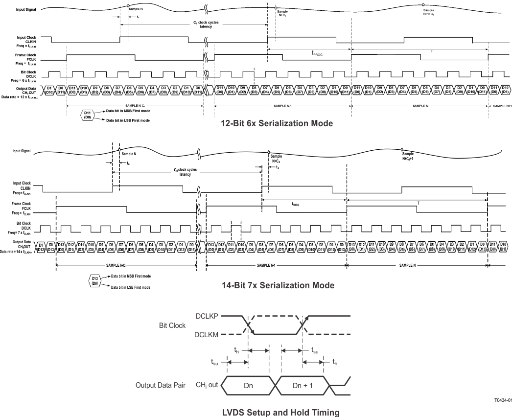 Figure 1. LVDS Timing Diagrams
7.11 Typical Characteristics
AVDD_5 V = 5 V, AVDD = 3.3 V, AVDD_ADC = 1.8 V, DVDD = 1.8 V, AC-coupled with 0.1-µF capacitors at INP and 15-nF capacitors at INM, No active termination, VCNTL = 0 V, FIN = 5 MHz, LNA = 18 dB, PGA = 24 dB, 14 bit, sample rate = 65 MSPS, LPF filter = 15 MHz, low-noise mode, Single-ended VCNTL mode, VCNTLM = GND, ADC is configured in internal reference mode, VOUT = –1 dBFS, 500-Ω CW feedback resistor, CMOS 16× clock, digital demodulator is disabled, at ambient temperature TA = 25°C, unless otherwise noted.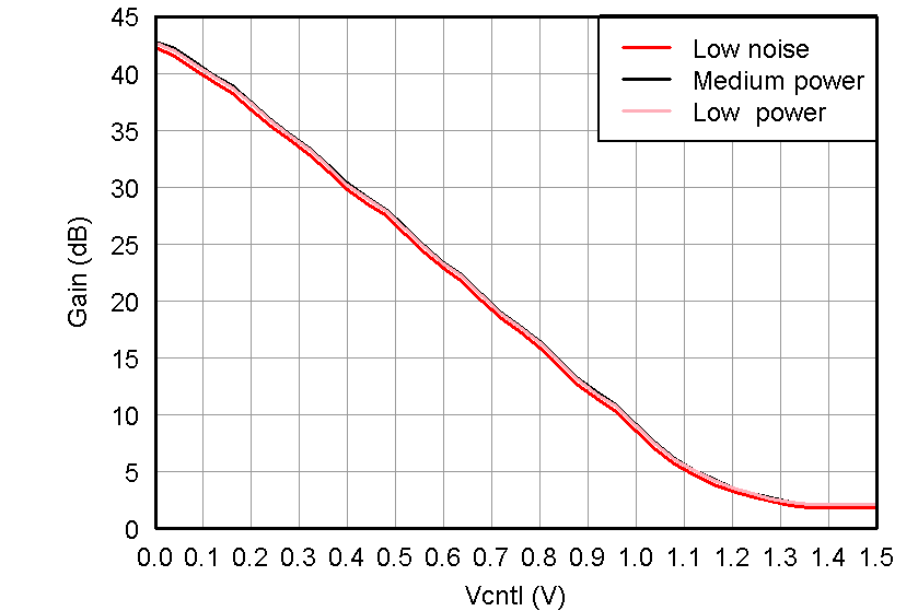 Figure 2. Gain vs VCNTL, LNA = 18 dB and PGA = 24 dB
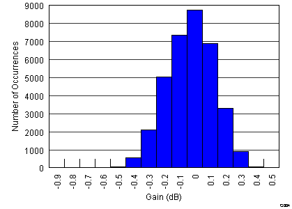 Figure 4. Gain Matching Histogram, VCNTL = 0.3 V (34951 Channels)
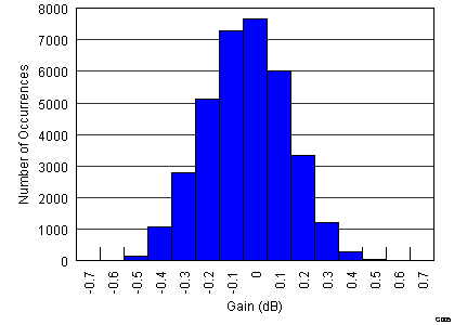 Figure 6. Gain Matching Histogram, VCNTL = 0.9 V (34951 Channels)
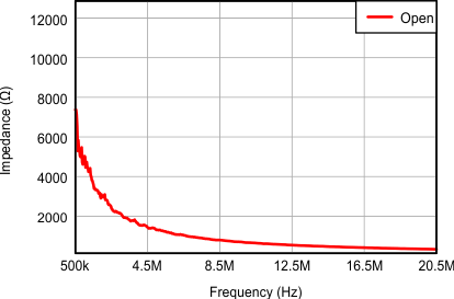 Figure 8. Input Impedance Without Active Termination (Magnitude)
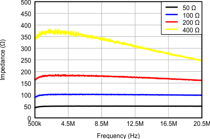 Figure 10. Input Impedance With Active Termination (Magnitude)
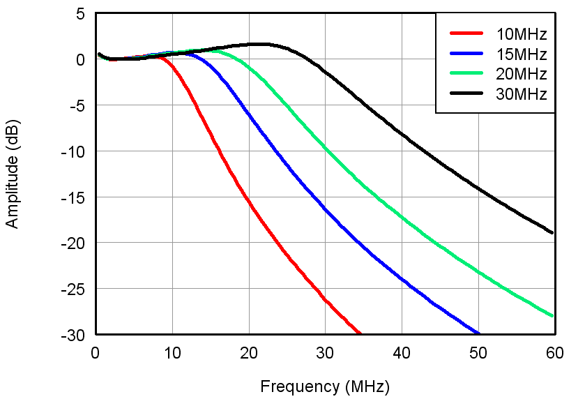 Figure 12. LPF Response
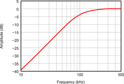 Figure 14. Full Channel HPF Response at Default Register Setting
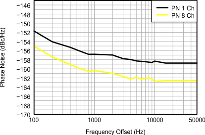 Figure 16. CW Phase Noise, FIN = 2 MHz, 1 Channel vs 8 Channel
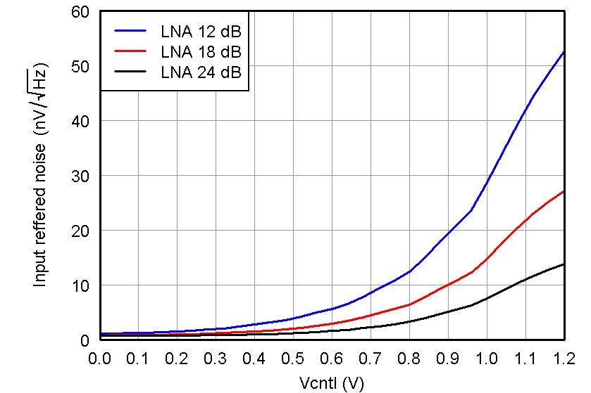 Figure 18. IRN, PGA = 24 dB and Low Noise Mode
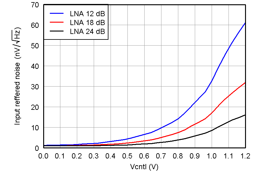 Figure 20. IRN, PGA = 24 dB and Medium-Power Mode
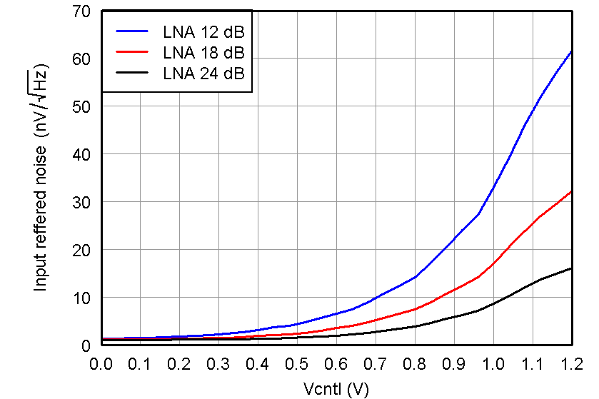 Figure 22. IRN, PGA = 24 dB and Low-Power Mode
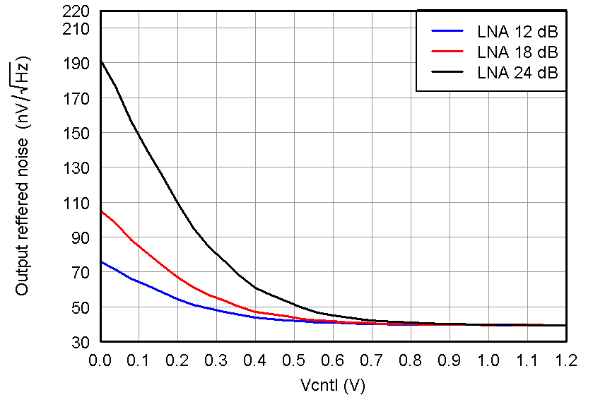 Figure 24. ORN, PGA = 24 dB and Low Noise Mode
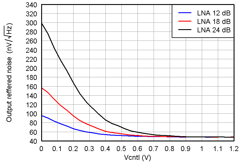 Figure 26. ORN, PGA = 24 dB and Low-Power Mode
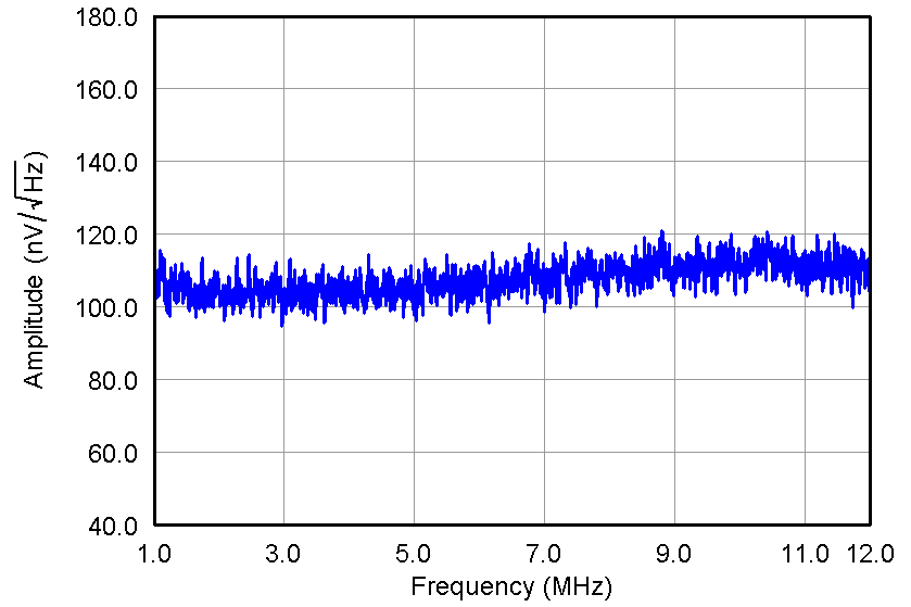 Figure 28. ORN, PGA = 24 dB and Low Noise Mode
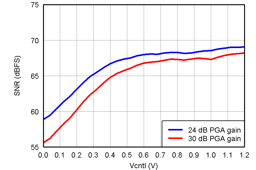 Figure 30. SNR, LNA = 18 dB and Low-Power Mode
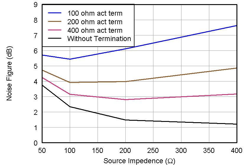 Figure 32. Noise Figure, LNA = 12 dB and Low Noise Mode
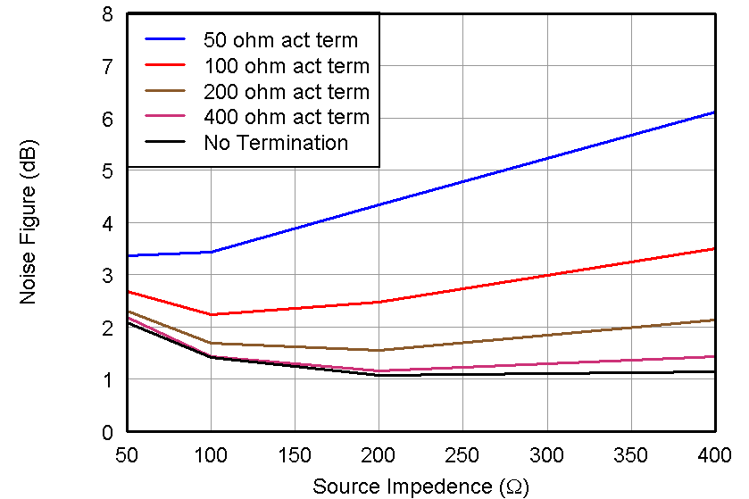 Figure 34. Noise Figure, LNA = 24 dB and Low Noise Mode
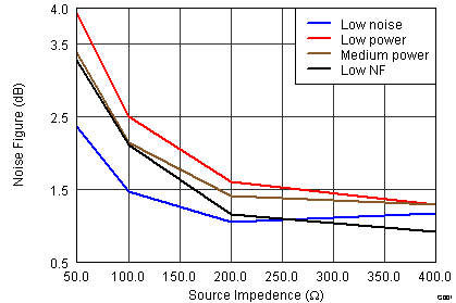 Figure 36. Noise Figure vs Power Modes Without Termination
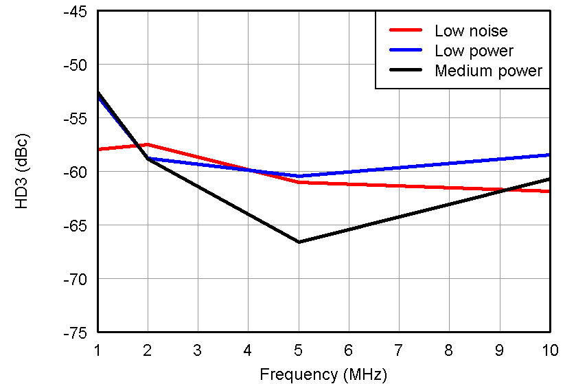 Figure 38. HD3 vs Frequency, VIN = 500 mVpp and
 VOUT = –1 dBFS
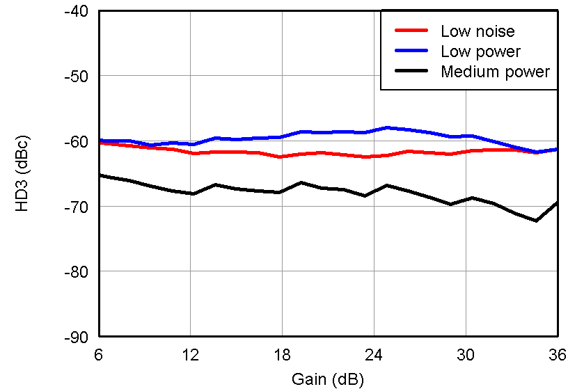 Figure 40. HD3 vs Gain, LNA = 12 dB and PGA = 24 dB and VOUT = –1 dBFS
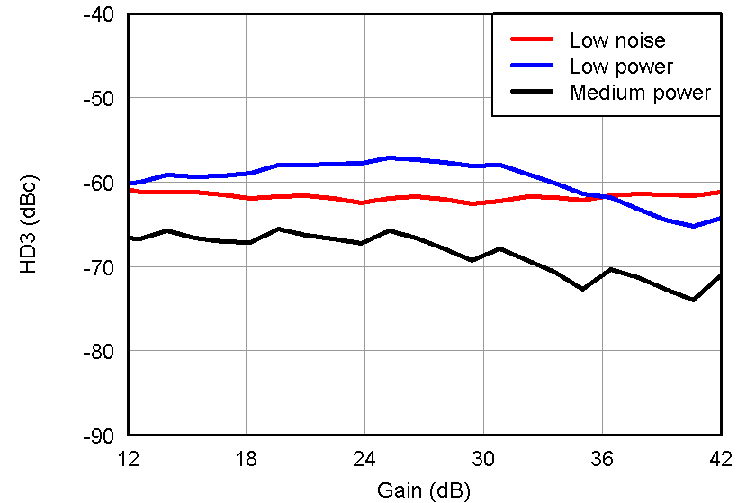 Figure 42. HD3 vs Gain, LNA = 18 dB and PGA = 24 dB and VOUT = –1 dBFS
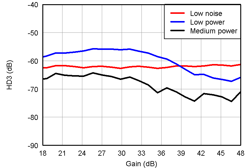 Figure 44. HD3 vs Gain, LNA = 24 dB and PGA = 24 dB and VOUT = –1 dBFS
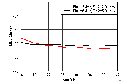 Figure 46. IMD3, Fout1 = –7 dBFS and Fout2 = –7 dBFS
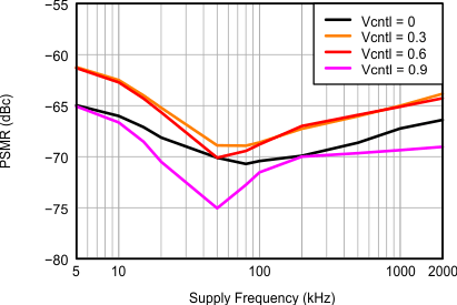 Figure 48. AVDD_5V Power Supply Modulation Ratio,
 100 mVpp Supply Noise With Different Frequencies
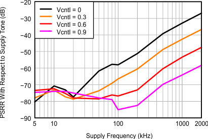 Figure 50. AVDD_5V Power Supply Rejection Ratio,
 100 mVpp Supply Noise With Different Frequencies
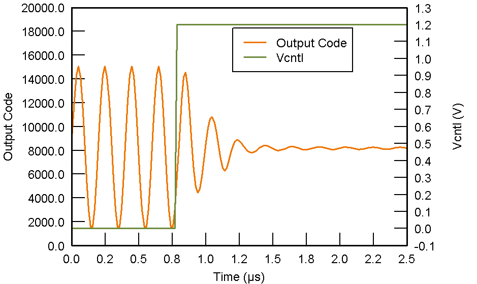
PGA = 24 dB
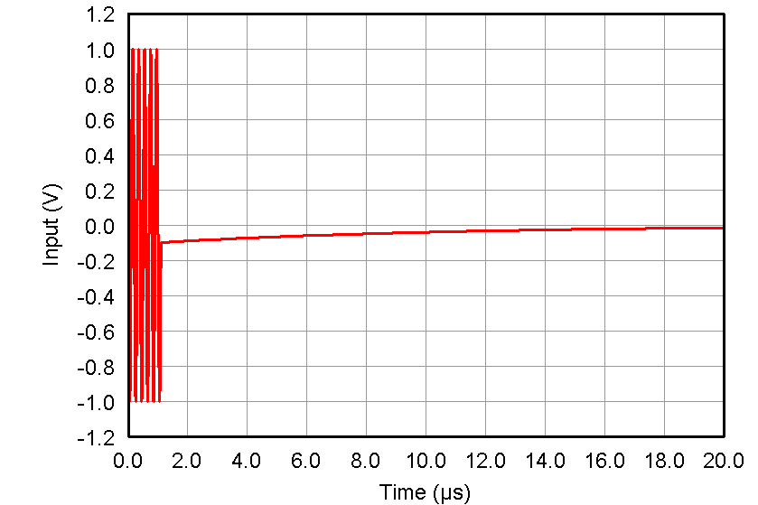 Figure 54. Pulse Inversion Asymmetrical Negative Input
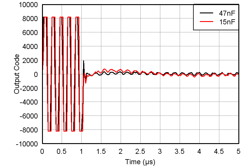 Figure 56. Overload Recovery Response vs INM Capacitor, VIN = 50 mVpp/100 µVpp, Max Gain
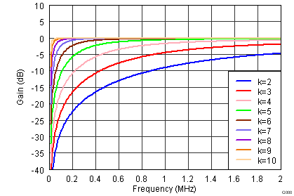 Figure 58. Digital HPF Response
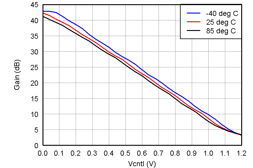 Figure 3. Gain Variation vs Temperature, LNA = 18 dB and PGA = 24 dB
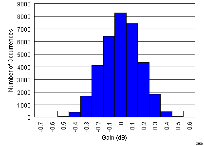 Figure 5. Gain Matching Histogram, VCNTL = 0.6 V (34951 Channels)
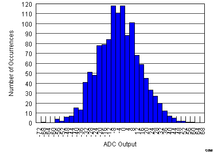 Figure 7. Output Offset Histogram, VCNTL = 0 V (1247 Channels)
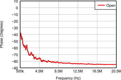 Figure 9. Input Impedance Without Active Termination (Phase)
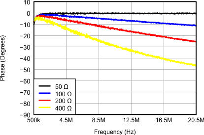 Figure 11. Input Impedance With Active Termination (Phase)
![AFE5809 LNA HPF Response vs
Reg59[3:2] AFE5809 gr_hpf_vcaoff_LOS738.gif](/ods/images/SLOS738E/gr_hpf_vcaoff_LOS738.gif) Figure 13. LNA HPF Response vs Reg59[3:2]
Figure 13. LNA HPF Response vs Reg59[3:2]
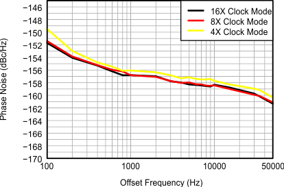 Figure 15. CW Phase Noise, FIN = 2 MHz
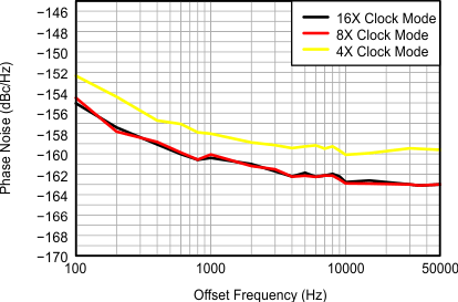 Figure 17. CW Phase Noise vs Clock Modes, FIN= 2 MHz
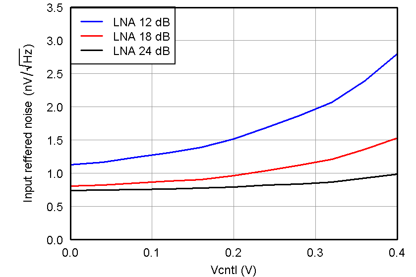 Figure 19. IRN, PGA = 24 dB and Low Noise Mode
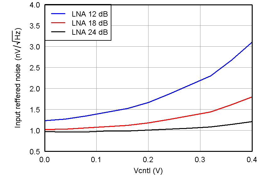 Figure 21. IRN, PGA = 24 dB and Medium-Power Mode
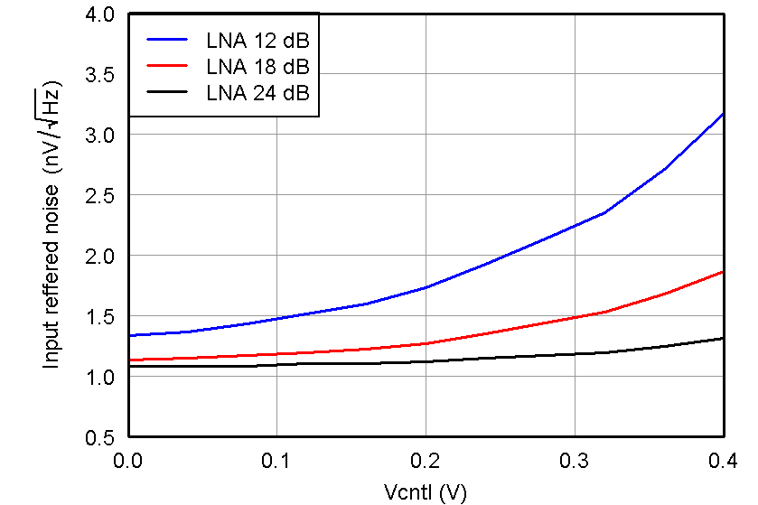 Figure 23. IRN, PGA = 24 dB and Low-Power Mode
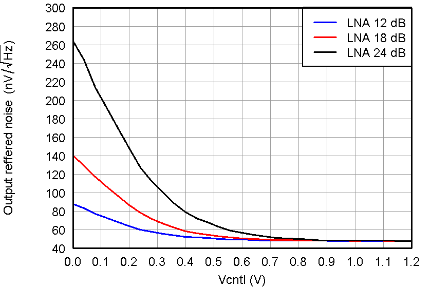 Figure 25. ORN, PGA = 24 dB and Medium-Power Mode
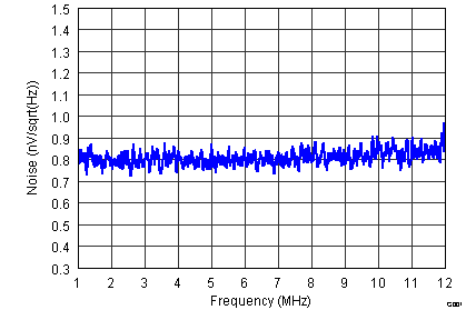 Figure 27. IRN, PGA = 24 dB and Low Noise Mode
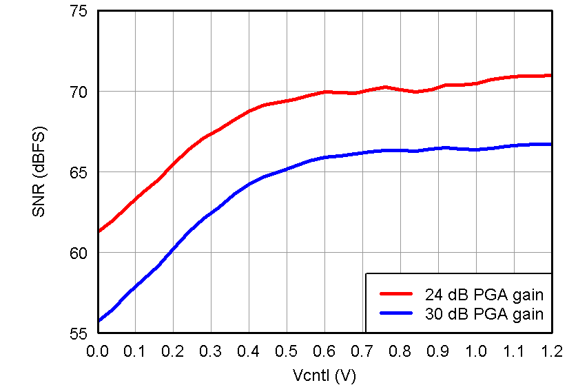 Figure 29. SNR, LNA = 18 dB and Low Noise Mode
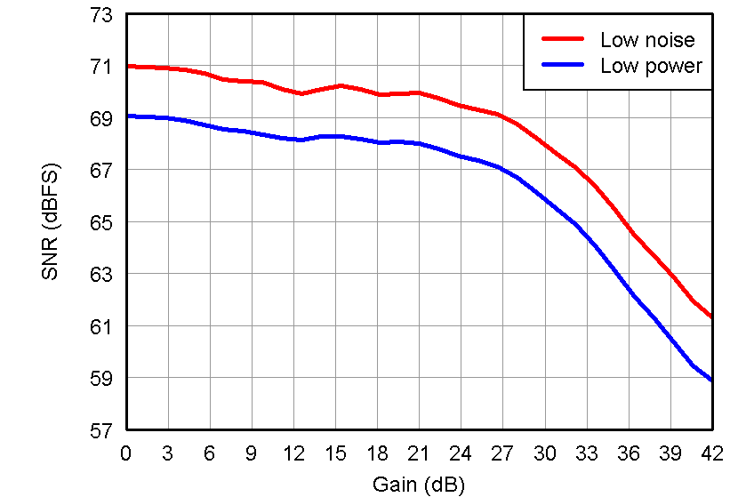 Figure 31. SNR vs Different Power Modes
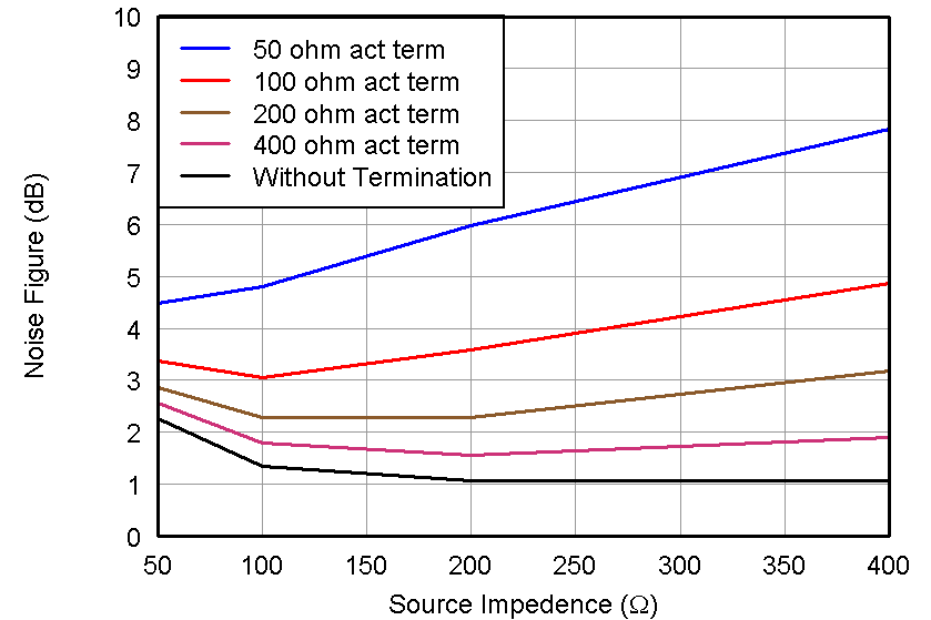 Figure 33. Noise Figure, LNA = 18 dB and Low Noise Mode
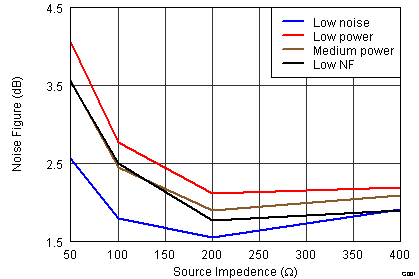 Figure 35. Noise Figure vs Power Modes With 400-Ω Termination
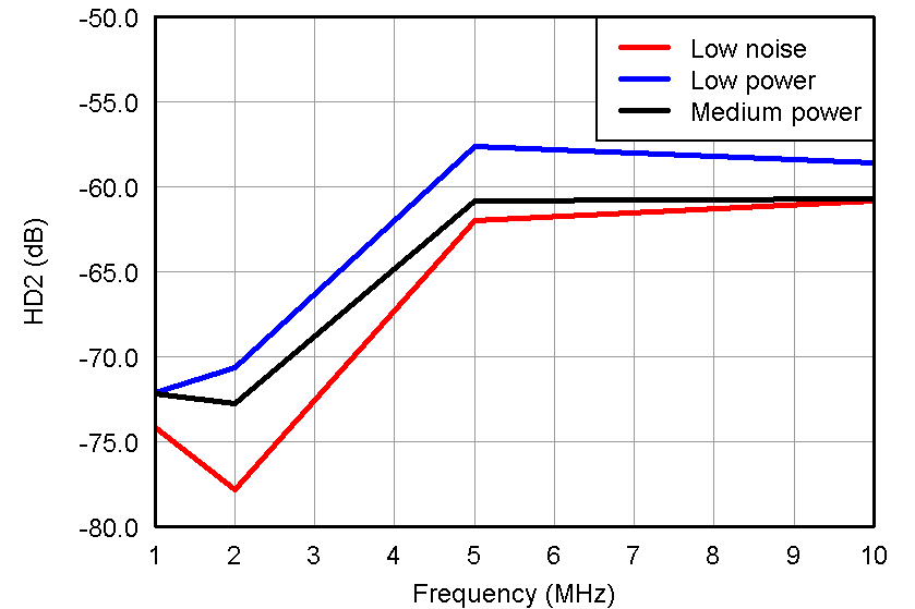 Figure 37. HD2 vs Frequency, VIN = 500 mVpp and
VOUT = –1 dBFS
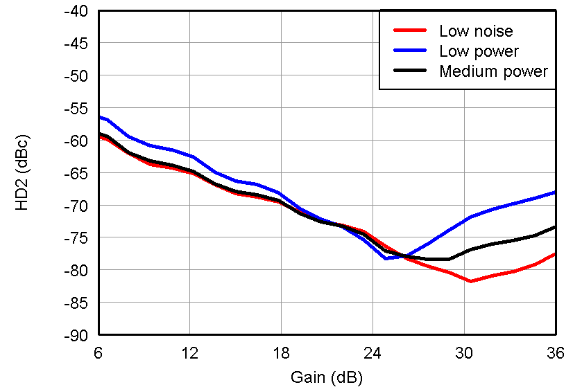 Figure 39. HD2 vs Gain, LNA = 12 dB and PGA = 24 dB and VOUT = –1 dBFS
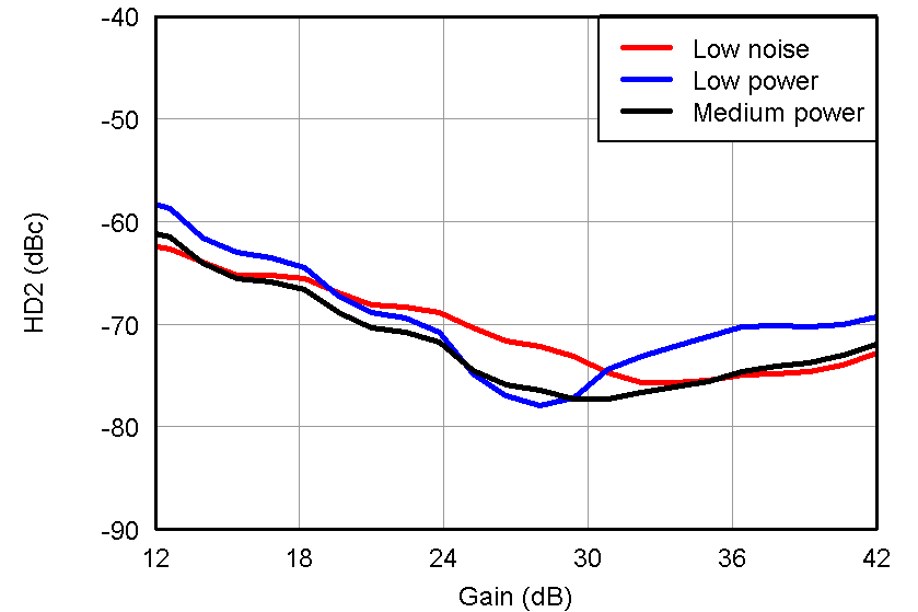 Figure 41. HD2 vs Gain, LNA = 18 dB and PGA = 24 dB and VOUT = –1 dBFS
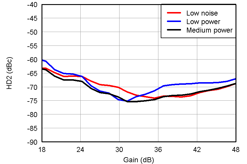 Figure 43. HD2 vs Gain, LNA = 24 dB and PGA = 24 dB and VOUT = –1 dBFS
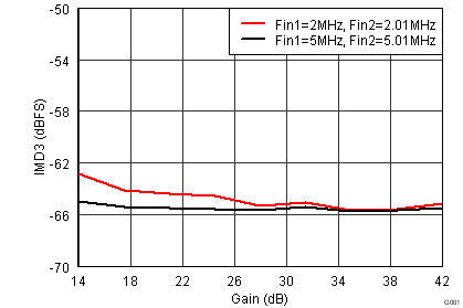 Figure 45. IMD3, Fout1 = –7 dBFS and Fout2 = –21 dBFS
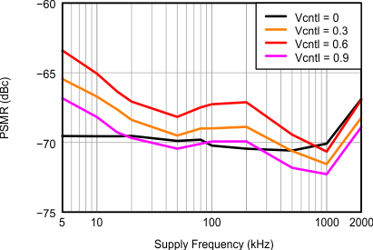 Figure 47. AVDD Power Supply Modulation Ratio, 100 mVpp Supply Noise With Different Frequencies
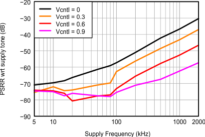 Figure 49. AVDD Power Supply Rejection Ratio, 100 mVpp Supply Noise With Different Frequencies
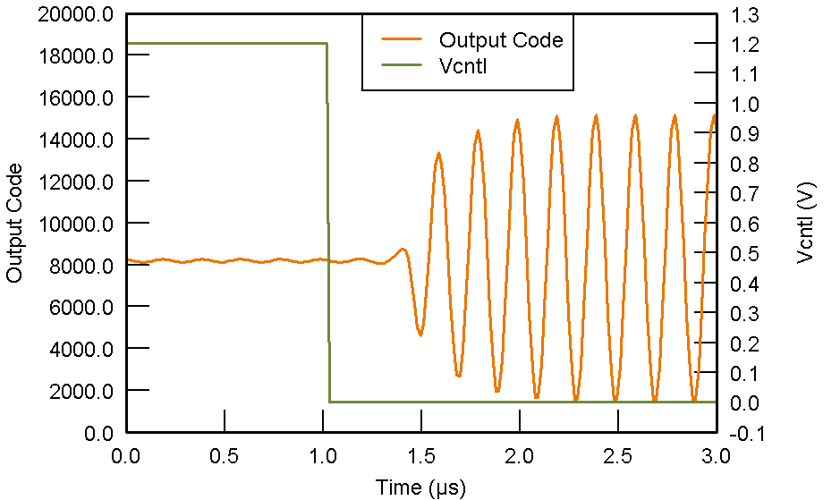
PGA = 24 dB
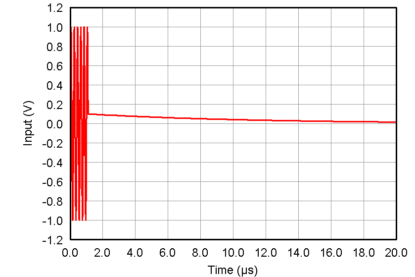 Figure 53. Pulse Inversion Asymmetrical Positive Input
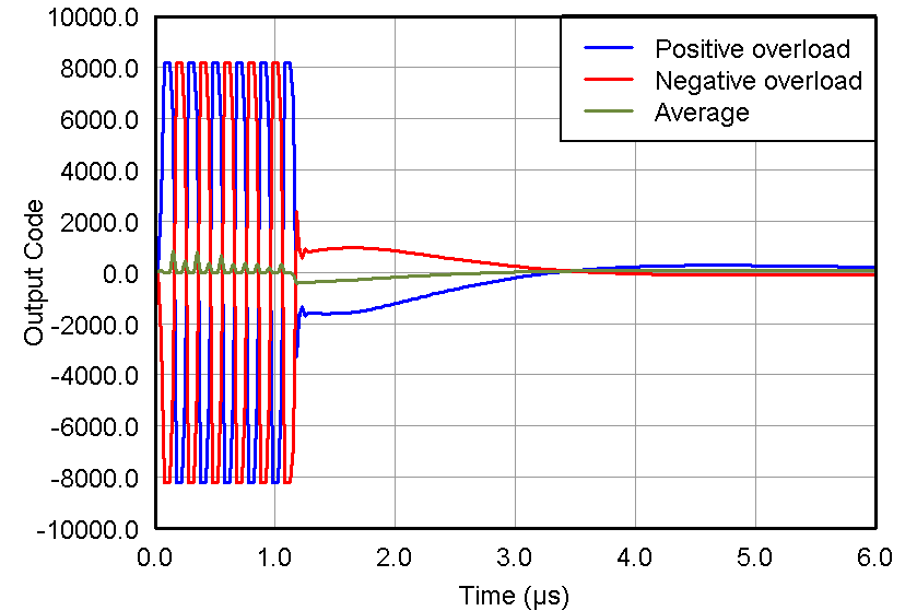 Figure 55. Pulse Inversion, VIN = 2 Vpp, PRF = 1 kHz,
 Gain = 21 dB
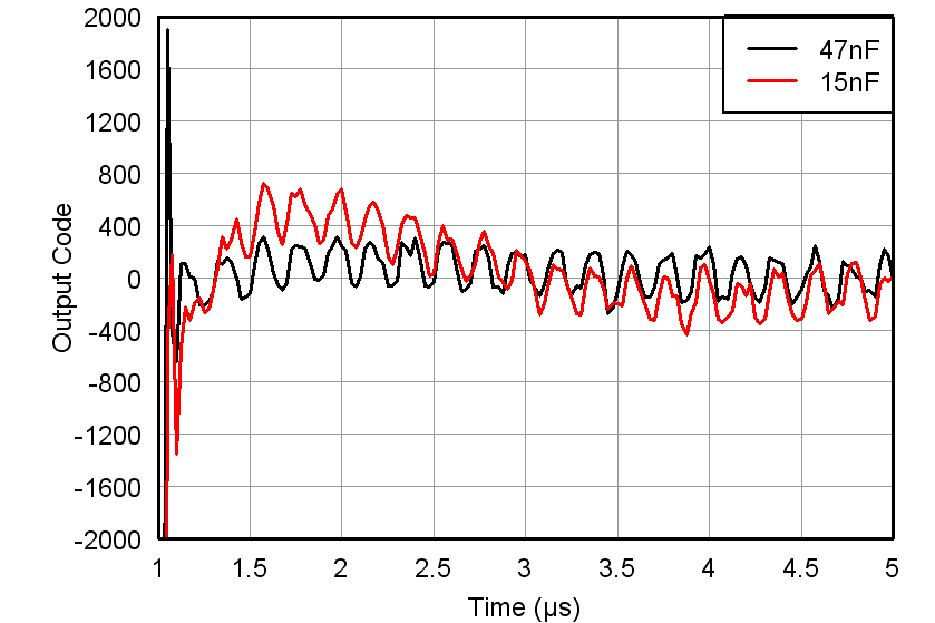 Figure 57. Overload Recovery Response vs INM Capacitor (Zoomed), VIN = 50 mVpp/100 µVpp, Max Gain
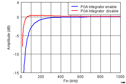 Figure 59. Signal Chain Low Frequency Response With INM Capacitor = 1 µF