SLLS114M January 1979 – March 2024 AM26LS31 , AM26LS31M
PRODUCTION DATA
- 1
- 1 Features
- 2 Applications
- 3 Description
- 4 Pin Configuration and Functions
- 5 Specifications
- 6 Parameter Measurement Information
- 7 Detailed Description
- 8 Application and Implementation
- 9 Device and Documentation Support
- 10Revision History
- 11Mechanical, Packaging, and Orderable Information
Package Options
Mechanical Data (Package|Pins)
Thermal pad, mechanical data (Package|Pins)
Orderable Information
3 Description
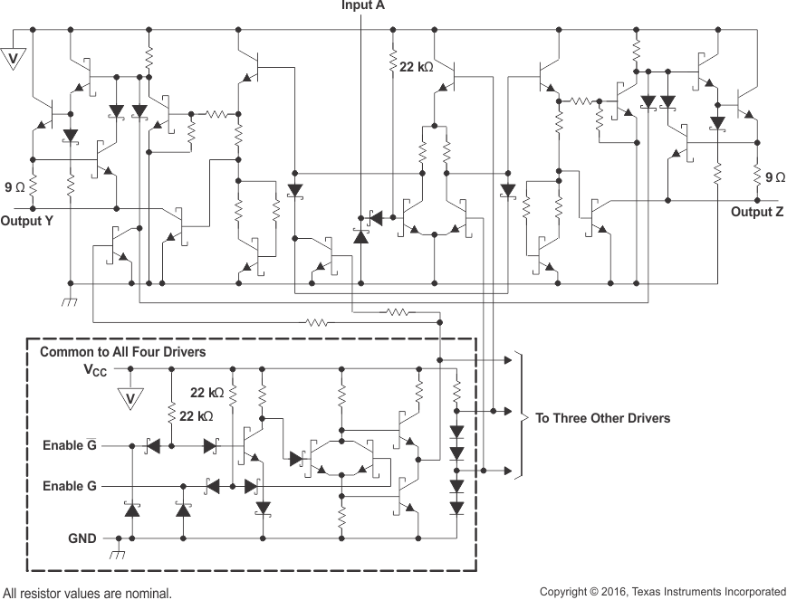
The AM26LS31CN-E family of devices is a quadruple complementary-output line driver designed to meet the requirements of ANSI TIA/EIA-422-B and ITU (formerly CCITT) Recommendation V.11. The 3-state outputs have high-current capability for driving balanced lines such as twisted-pair or parallel-wire transmission lines, and are in the high-impedance state in the power-off condition. The enable function is common to all four drivers and offers the choice of an active-high or active-low enable (G, G) input. Low-power Schottky circuitry reduces power consumption without sacrificing speed.
| PART NUMBER | PACKAGE(1) | PACKAGE SIZE(2) |
|---|---|---|
| AM26LS31MFK | LCCC (20) | 8.89mm × 8.89mm |
| AM26LS31MJ | CDIP (16) | 19.6mm × 6.92mm |
| AM26LS31MW | CFP (16) | 10.3mm × 6.73mm |
| AM26LS31CD | SOIC (16) | 9.9mm × 3.91mm |
| AM26LS31CDB | SSOP (16) | 6.2mm × 5.3mm |
| AM26LS31CN-E | PDIP (16) | 19.3mm × 6.35mm |
| AM26LS31xNS | SO (16) | 10.3mm × 5.3mm |
 Schematic (Each Driver)