SPRS695D September 2011 – January 2016 AM3871 , AM3874
PRODUCTION DATA.
- 1High-Performance System-on-Chip (SoC)
-
2Revision History
- 2.1 Device Comparison
- 2.2 Device Characteristics
- 2.3 Device Compatibility
- 2.4 ARM Cortex-A8 Microprocessor Unit (MPU) Subsystem Overview
- 2.5 Media Controller Overview
- 2.6 SGX530 Overview
- 2.7 Spinlock Module Overview
- 2.8 Mailbox Module Overview
- 2.9 Memory Map Summary
- 2.10 Pin Maps
- 2.11
Terminal Functions
- 2.11.1 Boot Configuration
- 2.11.2 Camera Interface (I/F)
- 2.11.3 Controller Area Network (DCAN) Modules (DCAN0, DCAN1)
- 2.11.4 DDR2/DDR3 Memory Controller
- 2.11.5 EDMA
- 2.11.6 EMAC [(R)(G)MII Modes] and MDIO
- 2.11.7 General-Purpose Input/Outputs (GPIOs)
- 2.11.8 GPMC
- 2.11.9 HDMI
- 2.11.10 I2C
- 2.11.11 McASP
- 2.11.12 McBSP
- 2.11.13 PCI-Express (PCIe)
- 2.11.14 Reset, Interrupts, and JTAG Interface
- 2.11.15 Serial ATA (SATA) Signals
- 2.11.16 SD Signals (MMC/SD/SDIO)
- 2.11.17 SPI
- 2.11.18 Oscillator/PLL, Audio Reference Clocks, and Clock Generator
- 2.11.19 Timer
- 2.11.20 UART
- 2.11.21 USB
- 2.11.22 Video Input (Digital)
- 2.11.23 Video Output (Digital)
- 2.11.24 Video Output (Analog, TV)
- 2.11.25 Reserved Pins
- 2.11.26 Supply Voltages
- 2.11.27 Ground Pins (VSS)
- 3Device Configurations
- 4 System Interconnect
- 5Device Operating Conditions
-
6Power, Reset, Clocking, and Interrupts
- 6.1 Power, Reset and Clock Management (PRCM) Module
- 6.2 Power
- 6.3
Reset
- 6.3.1 System-Level Reset Sources
- 6.3.2 Power-on Reset (POR pin)
- 6.3.3 External Warm Reset (RESET pin)
- 6.3.4 Emulation Warm Reset
- 6.3.5 Watchdog Reset
- 6.3.6 Software Global Cold Reset
- 6.3.7 Software Global Warm Reset
- 6.3.8 Test Reset (TRST pin)
- 6.3.9 Local Reset
- 6.3.10 Reset Priority
- 6.3.11 Reset Status Register
- 6.3.12 PCIE Reset Isolation
- 6.3.13 EMAC Switch Reset Isolation
- 6.3.14 RSTOUT_WD_OUT Pin
- 6.3.15 Effect of Reset on Emulation and Trace
- 6.3.16 Reset During Power Domain Switching
- 6.3.17 Pin Behaviors at Reset
- 6.3.18 Reset Electrical Data/Timing
- 6.4 Clocking
- 6.5 Interrupts
-
7 Peripheral Information and Timings
- 7.1 Parameter Information
- 7.2 Recommended Clock and Control Signal Transition Behavior
- 7.3 Controller Area Network Interface (DCAN)
- 7.4 EDMA
- 7.5 Emulation Features and Capability
- 7.6 Ethernet MAC Switch (EMAC SW)
- 7.7 General-Purpose Input/Output (GPIO)
- 7.8 General-Purpose Memory Controller (GPMC) and Error Location Module (ELM)
- 7.9 High-Definition Multimedia Interface (HDMI)
- 7.10 High-Definition Video Processing Subsystem (HDVPSS)
- 7.11 Inter-Integrated Circuit (I2C)
- 7.12 Imaging Subsystem (ISS)
- 7.13
DDR2/DDR3 Memory Controller
- 7.13.1 DDR2/3 Memory Controller Register Descriptions
- 7.13.2 DDR2/DDR3 PHY Register Descriptions
- 7.13.3 DDR-Related Control Module Registers Description
- 7.13.4
DDR2/DDR3 Memory Controller Electrical Data/Timing
- 7.13.4.1
DDR2 Routing Specifications
- 7.13.4.1.1
DDR2 Interface
- 7.13.4.1.1.1 DDR2 Interface Schematic
- 7.13.4.1.1.2 Compatible JEDEC DDR2 Devices
- 7.13.4.1.1.3 PCB Stackup
- 7.13.4.1.1.4 Placement
- 7.13.4.1.1.5 DDR2 Keepout Region
- 7.13.4.1.1.6 Bulk Bypass Capacitors
- 7.13.4.1.1.7 High-Speed Bypass Capacitors
- 7.13.4.1.1.8 Net Classes
- 7.13.4.1.1.9 DDR2 Signal Termination
- 7.13.4.1.1.10 VREFSSTL_DDR Routing
- 7.13.4.1.2 DDR2 CK and ADDR_CTRL Routing
- 7.13.4.1.1
DDR2 Interface
- 7.13.4.2
DDR3 Routing Specifications
- 7.13.4.2.1 DDR3 versus DDR2
- 7.13.4.2.2 DDR3 EMIFs
- 7.13.4.2.3 DDR3 Device Combinations
- 7.13.4.2.4
DDR3 Interface Schematic
- 7.13.4.2.4.1 Compatible JEDEC DDR3 Devices
- 7.13.4.2.4.2 PCB Stackup
- 7.13.4.2.4.3 Placement
- 7.13.4.2.4.4 DDR3 Keepout Region
- 7.13.4.2.4.5 Bulk Bypass Capacitors
- 7.13.4.2.4.6 High-Speed Bypass Capacitors
- 7.13.4.2.4.7 Net Classes
- 7.13.4.2.4.8 DDR3 Signal Termination
- 7.13.4.2.4.9 VREFSSTL_DDR Routing
- 7.13.4.2.4.10 VTT
- 7.13.4.2.4.11 CK and ADDR_CTRL Topologies and Routing Definition
- 7.13.4.2.4.12 Data Topologies and Routing Definition
- 7.13.4.2.4.13 Routing Specification
- 7.13.4.1
DDR2 Routing Specifications
- 7.14 Multichannel Audio Serial Port (McASP)
- 7.15 Multichannel Buffered Serial Port (McBSP)
- 7.16 MultiMedia Card/Secure Digital/Secure Digital Input Output (MMC/SD/SDIO)
- 7.17 Peripheral Component Interconnect Express (PCIe)
- 7.18 Serial ATA Controller (SATA)
- 7.19 Serial Peripheral Interface (SPI)
- 7.20 Timers
- 7.21 Universal Asynchronous Receiver/Transmitter (UART)
- 7.22 Universal Serial Bus (USB2.0)
- 8Device and Documentation Support
- 9Mechanical, Packaging, and Orderable Information
Package Options
Refer to the PDF data sheet for device specific package drawings
Mechanical Data (Package|Pins)
- CYE|684
Thermal pad, mechanical data (Package|Pins)
Orderable Information
7 Peripheral Information and Timings
7.1 Parameter Information
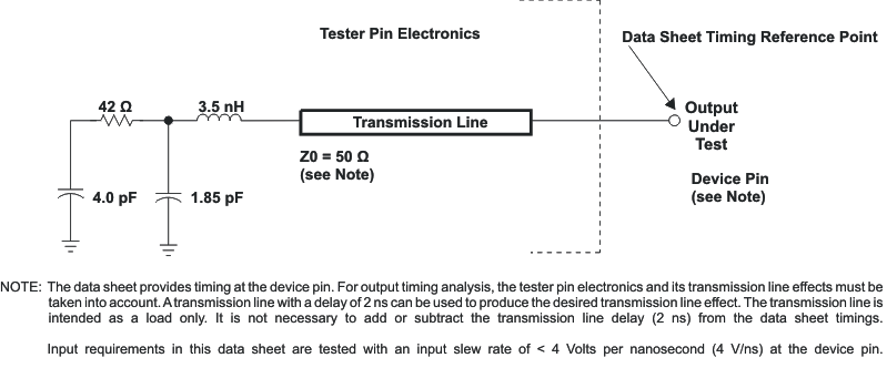 Figure 7-1 Test Load Circuit for AC Timing Measurements
The load capacitance value stated is only for characterization and measurement of AC timing signals. This load capacitance value does not indicate the maximum load the device is capable of driving.
7.1.1 1.8-V and 3.3-V Signal Transition Levels
All input and output timing parameters are referenced to Vref for both "0" and "1" logic levels. For 3.3-V I/O, Vref = 1.5 V. For 1.8-V I/O, Vref = 0.9 V.
 Figure 7-2 Input and Output Voltage Reference Levels for AC Timing Measurements
All rise and fall transition timing parameters are referenced to VIL MAX and VIH MIN for input clocks, VOL MAX and VOH MIN for output clocks.
 Figure 7-3 Rise and Fall Transition Time Voltage Reference Levels
7.1.2 3.3-V Signal Transition Rates
All timings are tested with an input edge rate of 4 volts per nanosecond (4 V/ns).
7.1.3 Timing Parameters and Board Routing Analysis
The timing parameter values specified in this data manual do not include delays by board routings. As a good board design practice, such delays must always be taken into account. Timing values may be adjusted by increasing/decreasing such delays. TI recommends utilizing the available I/O buffer information specification (IBIS) models to analyze the timing characteristics correctly. To properly use IBIS models to attain accurate timing analysis for a given system, see the Using IBIS Models for Timing Analysis application report (Literature Number: SPRA839). If needed, external logic hardware such as buffers may be used to compensate any timing differences.
7.2 Recommended Clock and Control Signal Transition Behavior
All clocks and control signals must transition between VIH and VIL (or between VIL and VIH) in a monotonic manner.
7.3 Controller Area Network Interface (DCAN)
The device provides two DCAN interfaces for supporting distributed realtime control with a high level of security. The DCAN interfaces implement the following features:
- Supports CAN protocol version 2.0 part A, B
- Bit rates up to 1 MBit/s
- 64 message objects
- Individual identifier mask for each message object
- Programmable FIFO mode for message objects
- Programmable loop-back modes for self-test operation
- Suspend mode for debug support
- Software module reset
- Automatic bus on after Bus-Off state by a programmable 32-bit timer
- Message RAM parity check mechanism
- Direct access to Message RAM during test mode
- CAN Rx/Tx pins are configurable as general-purpose IO pins
- Two interrupt lines (plus additional parity-error interrupts line)
- RAM initialization
- DMA support
For more detailed information on the DCAN peripheral, see the DCAN Controller Area Network chapter of the AM387x Sitara™ ARM Processors Technical Reference Manual (Literature Number: SPRUGZ7).
7.3.1 DCAN Peripheral Register Descriptions
7.3.2 DCAN Electrical Data/Timing
Table 7-1 Timing Requirements for DCANx Receive(1) (see Figure 7-4)
| NO. | OPP100/120/166 | UNIT | ||||
|---|---|---|---|---|---|---|
| MIN | NOM | MAX | ||||
| f(baud) | Maximum programmable baud rate | 1 | Mbps | |||
| 1 | tw(DCANRX) | Pulse duration, receive data bit (DCANx_RX) | H - 2 | H + 2 | ns | |
Table 7-2 Switching Characteristics Over Recommended Operating Conditions for DCANx Transmit (1)(see Figure 7-4)
| NO. | PARAMETER | OPP100/120/166 | UNIT | |||
|---|---|---|---|---|---|---|
| MIN | MAX | |||||
| f(baud) | Maximum programmable baud rate | 1 | Mbps | |||
| 2 | tw(DCANTX) | Pulse duration, transmit data bit (DCANx_TX) | H - 2 | H + 2 | ns | |
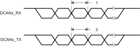 Figure 7-4 DCANx Timings
7.4 EDMA
The EDMA controller handles all data transfers between memories and the device slave peripherals on the device. These data transfers include cache servicing, noncacheable memory accesses, user-programmed data transfers, and host accesses.
7.4.1 EDMA Channel Synchronization Events
The EDMA Channel controller supports up to 64 channels that service peripherals and memory. Each EDMA channel is mapped to a defaul EDMA synchronization event as shown in Table 7-3. By default, each event uses the parameter entry that matches its event number. However, because the device includes a channel mapping feature, each event may be mapped to any of 512 parameter table entries. For more detailed information, see the Enhanced Direct Memory Access Controller chapter of the AM387x Sitara™ ARM Processors Technical Reference Manual (Literature Number: SPRUGZ7).
Table 7-3 EDMA Default Synchronization Events
| EVENT NUMBER |
DEFAULT EVENT NAME |
DEFAULT EVENT DESCRIPTION |
|---|---|---|
| 0-1 | – | Reserved |
| 2 | SDTXEVT1 | SD1 Transmit |
| 3 | SDRXEVT1 | SD1 Receive |
| 4-7 | – | Reserved |
| 8 | AXEVT0 | McASP0 Transmit |
| 9 | AREVT0 | McASP0 Receive |
| 10 | AXEVT1 | McASP1 Transmit |
| 11 | AREVT1 | McASP1 Receive |
| 12 | AXEVT2 | McASP2 Transmit |
| 13 | AREVT2 | McASP2 Receive |
| 14 | BXEVT | McBSP Transmit |
| 15 | BREVT | McBSP Receive |
| 16 | SPI0XEVT0 | SPI0 Transmit 0 |
| 17 | SPI0REVT0 | SPI0 Receive 0 |
| 18 | SPI0XEVT1 | SPI0 Transmit 1 |
| 19 | SPI0REVT1 | SPI0 Receive 1 |
| 20 | SPI0XEVT2 | SPI0 Transmit 2 |
| 21 | SPI0REVT2 | SPI0 Receive 2 |
| 22 | SPI0XEVT3 | SPI0 Transmit 3 |
| 23 | SPI0REVT3 | SPI0 Receive 3 |
| 24 | SDTXEVT0 | SD0 Transmit |
| 25 | SDRXEVT0 | SD0 Receive |
| 26 | UTXEVT0 | UART0 Transmit |
| 27 | URXEVT0 | UART0 Receive |
| 28 | UTXEVT1 | UART1 Transmit |
| 29 | URXEVT1 | UART1 Receive |
| 30 | UTXEVT2 | UART2 Transmit |
| 31 | URXEVT2 | UART2 Receive |
| 32-35 | – | Reserved |
| 36 | ISS_DMA_REQ1 | ISS Event 1 |
| 37 | ISS_DMA_REQ2 | ISS Event 2 |
| 38 | ISS_DMA_REQ3 | ISS Event 3 |
| 39 | ISS_DMA_REQ4 | ISS Event 4 |
| 40 | CAN_IF1DMA | DCAN0 IF1 |
| 41 | CAN_IF2DMA | DCAN0 IF2 |
| 42 | SPI1XEVT0 | SPI1 Transmit 0 |
| 43 | SPI1REVT0 | SPI1 Receive 0 |
| 44 | SPI1XEVT1 | SPI1 Transmit 1 |
| 45 | SPI1REVT1 | SPI1 Receive 1 |
| 46 | – | Reserved |
| 47 | CAN_IF3DMA | DCAN0 IF3 |
| 48 | TINT4 | TIMER4 |
| 49 | TINT5 | TIMER5 |
| 50 | TINT6 | TIMER6 |
| 51 | TINT7 | TIMER7 |
| 52 | GPMCEVT | GPMC |
| 53 | HDMIEVT | HDMI |
| 54 | – | Reserved |
| 55 | – | Reserved |
| 56 | AXEVT3 | McASP3 Transmit |
| 57 | AREVT3 | McASP3 Receive |
| 58 | I2CTXEVT0 | I2C0 Transmit |
| 59 | I2CRXEVT0 | I2C0 Receive |
| 60 | I2CTXEVT1 | I2C1 Transmit |
| 61 | I2CRXEVT1 | I2C1 Receive |
| 62 | AXEVT4 | McASP4 Transmit |
| 63 | AREVT4 | McASP4 Receive |
Table 7-4 EDMA Multiplexed Synchronization Events
| EVT_MUX_x VALUE |
MULTIPLEXED EVENT NAME |
MULTIPLEXED EVENT DESCRIPTION |
|---|---|---|
| 0 | - | Default Event |
| 1 | SDTXEVT2 | SD2 Transmit |
| 2 | SDRXEVT2 | SD2 Receive |
| 3 | I2CTXEVT2 | I2C2 Transmit |
| 4 | I2CRXEVT2 | I2C2 Receive |
| 5 | I2CTXEVT3 | I2C3 Transmit |
| 6 | I2CRXEVT3 | I2C3 Receive |
| 7 | UTXEVT3 | UART3 Transmit |
| 8 | URXEVT3 | UART3 Receive |
| 9 | UTXEVT4 | UART4 Transmit |
| 10 | URXEVT4 | UART4 Receive |
| 11 | UTXEVT5 | UART5 Transmit |
| 12 | URXEVT5 | UART5 Receive |
| 13 | CAN_IF1DMA | DCAN1 IF1 |
| 14 | CAN_IF2DMA | DCAN1 IF2 |
| 15 | CAN_IF3DMA | DCAN1 IF3 |
| 16 | SPI2XEVT0 | SPI2 Transmit 0 |
| 17 | SPI2REVT0 | SPI2 Receive 0 |
| 18 | SPI2XEVT1 | SPI2 Transmit 1 |
| 19 | SPI2REVT1 | SPI2 Receive 1 |
| 20 | SPI3XEVT0 | SPI3 Transmit 0 |
| 21 | SPI3REVT0 | SPI3 Receive 0 |
| 22 | – | Reserved |
| 23 | TINT1 | TIMER1 |
| 24 | TINT2 | TIMER2 |
| 25 | TINT3 | TIMER3 |
| 26 | AXEVT5 | McASP5 Transmit |
| 27 | AREVT5 | McASP5 Receive |
| 28 | EDMAEVT0 | EDMA_EVT0 Pin |
| 29 | EDMAEVT1 | EDMA_EVT1 Pin |
| 30 | EDMAEVT2 | EDMA_EVT2 Pin |
| 31 | EDMAEVT3 | EDMA_EVT3 Pin |
7.4.2 EDMA Peripheral Register Descriptions
Table 7-5 EDMA Channel Controller (EDMA TPCC) Control Registers
| HEX ADDRESS | ACRONYM | REGISTER NAME |
|---|---|---|
| 0x4900 0000 | PID | Peripheral Identification |
| 0x4900 0004 | CCCFG | EDMA3CC Configuration |
| 0x4900 0100 - 0x4900 01FC | DCHMAP0-63 | DMA Channel 0-63 Mappings |
| 0x4900 0200 | QCHMAP0 | QDMA Channel 0 Mapping |
| 0x4900 0204 | QCHMAP1 | QDMA Channel 1 Mapping |
| 0x4900 0208 | QCHMAP2 | QDMA Channel 2 Mapping |
| 0x4900 020C | QCHMAP3 | QDMA Channel 3 Mapping |
| 0x4900 0210 | QCHMAP4 | QDMA Channel 4 Mapping |
| 0x4900 0214 | QCHMAP5 | QDMA Channel 5 Mapping |
| 0x4900 0218 | QCHMAP6 | QDMA Channel 6 Mapping |
| 0x4900 021C | QCHMAP7 | QDMA Channel 7 Mapping |
| 0x4900 0240 | DMAQNUM0 | DMA Queue Number 0 |
| 0x4900 0244 | DMAQNUM1 | DMA Queue Number 1 |
| 0x4900 0248 | DMAQNUM2 | DMA Queue Number 2 |
| 0x4900 024C | DMAQNUM3 | DMA Queue Number 3 |
| 0x4900 0250 | DMAQNUM4 | DMA Queue Number 4 |
| 0x4900 0254 | DMAQNUM5 | DMA Queue Number 5 |
| 0x4900 0258 | DMAQNUM6 | DMA Queue Number 6 |
| 0x4900 025C | DMAQNUM7 | DMA Queue Number 7 |
| 0x4900 0260 | QDMAQNUM | QDMA Queue Number |
| 0x4900 0284 | QUEPRI | Queue Priority |
| 0x4900 0300 | EMR | Event Missed |
| 0x4900 0304 | EMRH | Event Missed High |
| 0x4900 0308 | EMCR | Event Missed Clear |
| 0x4900 030C | EMCRH | Event Missed Clear High |
| 0x4900 0310 | QEMR | QDMA Event Missed |
| 0x4900 0314 | QEMCR | QDMA Event Missed Clear |
| 0x4900 0318 | CCERR | EDMA3CC Error |
| 0x4900 031C | CCERRCLR | EDMA3CC Error Clear |
| 0x4900 0320 | EEVAL | Error Evaluate |
| 0x4900 0340 | DRAE0 | DMA Region Access Enable for Region 0 |
| 0x4900 0344 | DRAEH0 | DMA Region Access Enable High for Region 0 |
| 0x4900 0348 | DRAE1 | DMA Region Access Enable for Region 1 |
| 0x4900 034C | DRAEH1 | DMA Region Access Enable High for Region 1 |
| 0x4900 0350 | DRAE2 | DMA Region Access Enable for Region 2 |
| 0x4900 0354 | DRAEH2 | DMA Region Access Enable High for Region 2 |
| 0x4900 0358 | DRAE3 | DMA Region Access Enable for Region 3 |
| 0x4900 035C | DRAEH3 | DMA Region Access Enable High for Region 3 |
| 0x4900 0360 | DRAE4 | DMA Region Access Enable for Region 4 |
| 0x4900 0364 | DRAEH4 | DMA Region Access Enable High for Region 4 |
| 0x4900 0368 | DRAE5 | DMA Region Access Enable for Region 5 |
| 0x4900 036C | DRAEH5 | DMA Region Access Enable High for Region 5 |
| 0x4900 0370 | DRAE6 | DMA Region Access Enable for Region 6 |
| 0x4900 0374 | DRAEH6 | DMA Region Access Enable High for Region 6 |
| 0x4900 0378 | DRAE7 | DMA Region Access Enable for Region 7 |
| 0x4900 037C | DRAEH7 | DMA Region Access Enable High for Region 7 |
| 0x4900 0380 - 0x4900 039C | QRAE0-7 | QDMA Region Access Enable for Region 0-7 |
| 0x4900 0400 - 0x4900 04FC | Q0E0-Q3E15 | Event Queue Entry Q0E0-Q3E15 |
| 0x4900 0600 - 0x4900 060C | QSTAT0-3 | Queue Status 0-3 |
| 0x4900 0620 | QWMTHRA | Queue Watermark Threshold A |
| 0x4900 0640 | CCSTAT | EDMA3CC Status |
| 0x4900 0800 | MPFAR | Memory Protection Fault Address |
| 0x4900 0804 | MPFSR | Memory Protection Fault Status |
| 0x4900 0808 | MPFCR | Memory Protection Fault Command |
| 0x4900 080C | MPPAG | Memory Protection Page Attribute Global |
| 0x4900 0810 - 0x4900 082C | MPPA0-7 | Memory Protection Page Attribute 0-7 |
| 0x4900 1000 | ER | Event |
| 0x4900 1004 | ERH | Event High |
| 0x4900 1008 | ECR | Event Clear |
| 0x4900 100C | ECRH | Event Clear High |
| 0x4900 1010 | ESR | Event Set |
| 0x4900 1014 | ESRH | Event Set High |
| 0x4900 1018 | CER | Chained Event |
| 0x4900 101C | CERH | Chained Event High |
| 0x4900 1020 | EER | Event Enable |
| 0x4900 1024 | EERH | Event Enable High |
| 0x4900 1028 | EECR | Event Enable Clear |
| 0x4900 102C | EECRH | Event Enable Clear High |
| 0x4900 1030 | EESR | Event Enable Set |
| 0x4900 1034 | EESRH | Event Enable Set High |
| 0x4900 1038 | SER | Secondary Event |
| 0x4900 103C | SERH | Secondary Event High |
| 0x4900 1040 | SECR | Secondary Event Clear |
| 0x4900 1044 | SECRH | Secondary Event Clear High |
| 0x4900 1050 | IER | Interrupt Enable |
| 0x4900 1054 | IERH | Interrupt Enable High |
| 0x4900 1058 | IECR | Interrupt Enable Clear |
| 0x4900 105C | IECRH | Interrupt Enable Clear High |
| 0x4900 1060 | IESR | Interrupt Enable Set |
| 0x4900 1064 | IESRH | Interrupt Enable Set High |
| 0x4900 1068 | IPR | Interrupt Pending |
| 0x4900 106C | IPRH | Interrupt Pending High |
| 0x4900 1070 | ICR | Interrupt Clear |
| 0x4900 1074 | ICRH | Interrupt Clear High |
| 0x4900 1078 | IEVAL | Interrupt Evaluate |
| 0x4900 1080 | QER | QDMA Event |
| 0x4900 1084 | QEER | QDMA Event Enable |
| 0x4900 1088 | QEECR | QDMA Event Enable Clear |
| 0x4900 108C | QEESR | QDMA Event Enable Set |
| 0x4900 1090 | QSER | QDMA Secondary Event |
| 0x4900 1094 | QSECR | QDMA Secondary Event Clear |
| Shadow Region 0 Channel Registers | ||
| 0x4900 2000 | ER | Event |
| 0x4900 2004 | ERH | Event High |
| 0x4900 2008 | ECR | Event Clear |
| 0x4900 200C | ECRH | Event Clear High |
| 0x4900 2010 | ESR | Event Set |
| 0x4900 2014 | ESRH | Event Set High |
| 0x4900 2018 | CER | Chained Event |
| 0x4900 201C | CERH | Chained Event High |
| 0x4900 2020 | EER | Event Enable |
| 0x4900 2024 | EERH | Event Enable High |
| 0x4900 2028 | EECR | Event Enable Clear |
| 0x4900 202C | EECRH | Event Enable Clear High |
| 0x4900 2030 | EESR | Event Enable Set |
| 0x4900 2034 | EESRH | Event Enable Set High |
| 0x4900 2038 | SER | Secondary Event |
| 0x4900 203C | SERH | Secondary Event High |
| 0x4900 2040 | SECR | Secondary Event Clear |
| 0x4900 2044 | SECRH | Secondary Event Clear High |
| 0x4900 2050 | IER | Interrupt Enable |
| 0x4900 2054 | IERH | Interrupt Enable High |
| 0x4900 2058 | IECR | Interrupt Enable Clear |
| 0x4900 205C | IECRH | Interrupt Enable Clear High |
| 0x4900 2060 | IESR | Interrupt Enable Set |
| 0x4900 2064 | IESRH | Interrupt Enable Set High |
| 0x4900 2068 | IPR | Interrupt Pending |
| 0x4900 206C | IPRH | Interrupt Pending High |
| 0x4900 2070 | ICR | Interrupt Clear |
| 0x4900 2074 | ICRH | Interrupt Clear High |
| 0x4900 2078 | IEVAL | Interrupt Evaluate |
| 0x4900 2080 | QER | QDMA Event |
| 0x4900 2084 | QEER | QDMA Event Enable |
| 0x4900 2088 | QEECR | QDMA Event Enable Clear |
| 0x4900 208C | QEESR | QDMA Event Enable Set |
| 0x4900 2090 | QSER | QDMA Secondary Event |
| 0x4900 2094 | QSECR | QDMA Secondary Event Clear |
| 0x4900 2200 - 0x4900 2294 | - | Shadow Region 1 Channels |
| 0x4900 2400 - 0x4900 2494 | - | Shadow Region 2 Channels |
| ... | ... | |
| 0x4900 2E00 - 0x4900 2E94 | - | Shadow Channels for MP Space 7 |
Table 7-6 EDMA Transfer Controller (EDMA TPTC) Control Registers
| TPTC0 HEX ADDRESS | TPTC1 HEX ADDRESS | TPTC2 HEX ADDRESS | TPTC3 HEX ADDRESS | ACRONYM | REGISTER NAME |
|---|---|---|---|---|---|
| 0x4980 0000 | 0x4990 0000 | 0x49A0 0000 | 0x49B0 0000 | PID | Peripheral Identification |
| 0x4980 0004 | 0x4990 0004 | 0x49A0 0004 | 0x49B0 0004 | TCCFG | EDMA3TC Configuration |
| 0x4980 0100 | 0x4990 0100 | 0x49A0 0100 | 0x49B0 0100 | TCSTAT | EDMA3TC Channel Status |
| 0x4980 0120 | 0x4990 0120 | 0x49A0 0120 | 0x49B0 0120 | ERRSTAT | Error Status |
| 0x4980 0124 | 0x4990 0124 | 0x49A0 0124 | 0x49B0 0124 | ERREN | Error Enable |
| 0x4980 0128 | 0x4990 0128 | 0x49A0 0128 | 0x49B0 0128 | ERRCLR | Error Clear |
| 0x4980 012C | 0x4990 012C | 0x49A0 012C | 0x49B0 012C | ERRDET | Error Details |
| 0x4980 0130 | 0x4990 0130 | 0x49A0 0130 | 0x49B0 0130 | ERRCMD | Error Interrupt Command |
| 0x4980 0140 | 0x4990 0140 | 0x49A0 0140 | 0x49B0 0140 | RDRATE | Read Rate Register |
| 0x4980 0240 | 0x4990 0240 | 0x49A0 0240 | 0x49B0 0240 | SAOPT | Source Active Options |
| 0x4980 0244 | 0x4990 0244 | 0x49A0 0244 | 0x49B0 0244 | SASRC | Source Active Source Address |
| 0x4980 0248 | 0x4990 0248 | 0x49A0 0248 | 0x49B0 0248 | SACNT | Source Active Count |
| 0x4980 024C | 0x4990 024C | 0x49A0 024C | 0x49B0 024C | SADST | Source Active Destination Address |
| 0x4980 0250 | 0x4990 0250 | 0x49A0 0250 | 0x49B0 0250 | SABIDX | Source Active Source B-Index |
| 0x4980 0254 | 0x4990 0254 | 0x49A0 0254 | 0x49B0 0254 | SAMPPRXY | Source Active Memory Protection Proxy |
| 0x4980 0258 | 0x4990 0258 | 0x49A0 0258 | 0x49B0 0258 | SACNTRLD | Source Active Count Reload |
| 0x4980 025C | 0x4990 025C | 0x49A0 025C | 0x49B0 025C | SASRCBREF | Source Active Source Address B-Reference |
| 0x4980 0260 | 0x4990 0260 | 0x49A0 0260 | 0x49B0 0260 | SADSTBREF | Source Active Destination Address B-Reference |
| 0x4980 0280 | 0x4990 0280 | 0x49A0 0280 | 0x49B0 0280 | DFCNTRLD | Destination FIFO Set Count Reload |
| 0x4980 0284 | 0x4990 0284 | 0x49A0 0284 | 0x49B0 0284 | DFSRCBREF | Destination FIFO Set Destination Address B Reference |
| 0x4980 0288 | 0x4990 0288 | 0x49A0 0288 | 0x49B0 0288 | DFDSTBREF | Destination FIFO Set Destination Address B Reference |
| 0x4980 0300 | 0x4990 0300 | 0x49A0 0300 | 0x49B0 0300 | DFOPT0 | Destination FIFO Options 0 |
| 0x4980 0304 | 0x4990 0304 | 0x49A0 0304 | 0x49B0 0304 | DFSRC0 | Destination FIFO Source Address 0 |
| 0x4980 0308 | 0x4990 0308 | 0x49A0 0308 | 0x49B0 0308 | DFCNT0 | Destination FIFO Count 0 |
| 0x4980 030C | 0x4990 030C | 0x49A0 030C | 0x49B0 030C | DFDST0 | Destination FIFO Destination Address 0 |
| 0x4980 0310 | 0x4990 0310 | 0x49A0 0310 | 0x49B0 0310 | DFBIDX0 | Destination FIFO BIDX 0 |
| 0x4980 0314 | 0x4990 0314 | 0x49A0 0314 | 0x49B0 0314 | DFMPPRXY0 | Destination FIFO Memory Protection Proxy 0 |
| 0x4980 0340 | 0x4990 0340 | 0x49A0 0340 | 0x49B0 0340 | DFOPT1 | Destination FIFO Options 1 |
| 0x4980 0344 | 0x4990 0344 | 0x49A0 0344 | 0x49B0 0344 | DFSRC1 | Destination FIFO Source Address 1 |
| 0x4980 0348 | 0x4990 0348 | 0x49A0 0348 | 0x49B0 0348 | DFCNT1 | Destination FIFO Count 1 |
| 0x4980 034C | 0x4990 034C | 0x49A0 034C | 0x49B0 034C | DFDST1 | Destination FIFO Destination Address 1 |
| 0x4980 0350 | 0x4990 0350 | 0x49A0 0350 | 0x49B0 0350 | DFBIDX1 | Destination FIFO BIDX 1 |
| 0x4980 0354 | 0x4990 0354 | 0x49A0 0354 | 0x49B0 0354 | DFMPPRXY1 | Destination FIFO Memory Protection Proxy 1 |
| 0x4980 0380 | 0x4990 0380 | 0x49A0 0380 | 0x49B0 0380 | DFOPT2 | Destination FIFO Options 2 |
| 0x4980 0384 | 0x4990 0384 | 0x49A0 0384 | 0x49B0 0384 | DFSRC2 | Destination FIFO Source Address 2 |
| 0x4980 0388 | 0x4990 0388 | 0x49A0 0388 | 0x49B0 0388 | DFCNT2 | Destination FIFO Count 2 |
| 0x4980 038C | 0x4990 038C | 0x49A0 038C | 0x49B0 038C | DFDST2 | Destination FIFO Destination Address 2 |
| 0x4980 0390 | 0x4990 0390 | 0x49A0 0390 | 0x49B0 0390 | DFBIDX2 | Destination FIFO BIDX 2 |
| 0x4980 0394 | 0x4990 0394 | 0x49A0 0394 | 0x49B0 0394 | DFMPPRXY2 | Destination FIFO Memory Protection Proxy 2 |
| 0x4980 03C0 | 0x4990 03C0 | 0x49A0 03C0 | 0x49B0 03C0 | DFOPT3 | Destination FIFO Options 3 |
| 0x4980 03C4 | 0x4990 03C4 | 0x49A0 03C4 | 0x49B0 03C4 | DFSRC3 | Destination FIFO Source Address 3 |
| 0x4980 03C8 | 0x4990 03C8 | 0x49A0 03C8 | 0x49B0 03C8 | DFCNT3 | Destination FIFO Count 3 |
| 0x4980 03CC | 0x4990 03CC | 0x49A0 03CC | 0x49B0 03CC | DFDST3 | Destination FIFO Destination Address 3 |
| 0x4980 03D0 | 0x4990 03D0 | 0x49A0 03D0 | 0x49B0 03D0 | DFBIDX3 | Destination FIFO BIDX 3 |
| 0x4980 03D4 | 0x4990 03D4 | 0x49A0 03D4 | 0x49B0 03D4 | DFMPPRXY3 | Destination FIFO Memory Protection Proxy 3 |
7.5 Emulation Features and Capability
7.5.1 Advanced Event Triggering (AET)
The device supports Advanced Event Triggering (AET). This capability can be used to debug complex problems as well as understand performance characteristics of user applications. AET provides the following capabilities:
- Hardware Program Breakpoints: specify addresses or address ranges that can generate events such as halting the processor or triggering the trace capture.
- Data Watchpoints: specify data variable addresses, address ranges, or data values that can generate events such as halting the processor or triggering the trace capture.
- Counters: count the occurrence of an event or cycles for performance monitoring.
- State Sequencing: allows combinations of hardware program breakpoints and data watchpoints to precisely generate events for complex sequences.
For more information on AET, see the following documents:
7.5.2 Trace
The device supports Trace at the Cortex™-A8 and System levels. Trace is a debug technology that provides a detailed, historical account of application code execution, timing, and data accesses. Trace collects, compresses, and exports debug information for analysis. The debug information can be exported to the Embedded Trace Buffer (ETB), or to the 5-pin Trace Interface (system trace only). Trace works in real-time and does not impact the execution of the system.
For more information on board design guidelines for Trace Advanced Emulation, see the Emulation and Trace Headers Technical Reference Manual (Literature Number: SPRU655).
7.5.3 IEEE 1149.1 JTAG
The JTAG (IEEE Standard 1149.1-1990 Standard-Test-Access Port and Boundary Scan Architecture) interface is used for BSDL testing and emulation of the device. The TRST pin only must be released when it is necessary to use a JTAG controller to debug the device or exercise the boundary scan functionality of the device. For maximum reliability, the device includes an internal pulldown (IPD) on the TRST pin to ensure that TRST is always asserted upon power up and the internal emulation logic of the device is always properly initialized. JTAG controllers from Texas Instruments actively drive TRST high. However, some third-party JTAG controllers may not drive TRST high but expect the use of a pullup resistor on TRST. When using this type of JTAG controller, assert TRST to initialize the device after powerup and externally drive TRST high before attempting any emulation or boundary-scan operations.
The main JTAG features include:
- 32KB embedded trace buffer (ETB)
- 5-pin system trace interface for debug
- Supports Advanced Event Triggering (AET)
- All processors can be emulated via JTAG ports
- All functions on EMU pins of the device:
- EMU[1:0] - cross-triggering, boot mode (WIR), STM trace
- EMU[4:2] - STM trace only (single direction)
7.5.3.1 JTAG ID (JTAGID) Register Description
Table 7-7 JTAG ID Register(1)
| HEX ADDRESS | ACRONYM | REGISTER NAME |
|---|---|---|
| 0x4814 0600 | JTAGID | JTAG Identification Register(2) |
The JTAG ID register is a read-only register that identifies to the customer the JTAG/device ID. For this device, the JTAG ID register resides at address location 0x4814 0600. The register hex value for the device is: 0x0B8F 202F. For the actual register bit names and their associated bit field descriptions, see Figure 7-5 and Table 7-8.
| 31 | 30 | 29 | 28 | 27 | 26 | 25 | 24 | 23 | 22 | 21 | 20 | 19 | 18 | 17 | 16 | 15 | 14 | 13 | 12 | 11 | 10 | 9 | 8 | 7 | 6 | 5 | 4 | 3 | 2 | 1 | 0 |
| VARIANT (4-bit) | PART NUMBER (16-bit) | MANUFACTURER (11-bit) | LSB | ||||||||||||||||||||||||||||
| R-xxxx | R-1011 1000 1111 0010 | R-0000 0010 111 | R-1 | ||||||||||||||||||||||||||||
| LEGEND: R/W = Read/Write; R = Read only; -n = value after reset |
Table 7-8 JTAG ID Register Selection Bit Descriptions
| Bit | Field | Description |
|---|---|---|
| 31:28 | VARIANT | Variant (4-bit) value. Device value: xxxx. This value reflects the device silicon revision [For example, 0x0 (0000) for initial silicon revision (SR) 1.0].
|
| 27:12 | PART NUMBER | Part Number (16-bit) value. Device value: 0xB8F2 (1011 1000 1111 0010) |
| 11:1 | MANUFACTURER | Manufacturer (11-bit) value. Device value: 0x017 (0000 0010 111) |
| 0 | LSB | LSB. This bit is read as a ""1 for this device. |
7.5.3.2 JTAG Electrical Data/Timing
Table 7-9 Timing Requirements for IEEE 1149.1 JTAG
(see Figure 7-6)| NO. | OPP100/120/166 | UNIT | |||
|---|---|---|---|---|---|
| MIN | MAX | ||||
| 1 | tc(TCK) | Cycle time, TCK | 51.15 | ns | |
| 1a | tw(TCKH) | Pulse duration, TCK high (40% of tc) | 20.46 | ns | |
| 1b | tw(TCKL) | Pulse duration, TCK low (40% of tc) | 20.46 | ns | |
| 3 | tsu(TDI-TCK) | Input setup time, TDI valid to TCK high (20% of (tc * 0.5)) | 5.115 | ns | |
| 3 | tsu(TMS-TCK) | Input setup time, TMS valid to TCK high (20% of (tc * 0.5)) | 5.115 | ns | |
| 4 | th(TCK-TDI) | Input hold time, TDI valid from TCK high | 10 | ns | |
| th(TCK-TMS) | Input hold time, TMS valid from TCK high | 10 | ns | ||
Table 7-10 Switching Characteristics Over Recommended Operating Conditions for IEEE 1149.1 JTAG
(see Figure 7-6)| NO. | PARAMETER | OPP100/120/166 | UNIT | ||
|---|---|---|---|---|---|
| MIN | MAX | ||||
| 2 | td(TCKL-TDOV) | Delay time, TCK low to TDO valid | 0 | 23.575(1) | ns |
 Figure 7-6 JTAG Timing
Table 7-11 Timing Requirements for IEEE 1149.1 JTAG With RTCK
(see Figure 7-6)| NO. | OPP100/120/166 | UNIT | |||
|---|---|---|---|---|---|
| MIN | MAX | ||||
| 1 | tc(TCK) | Cycle time, TCK | 51.15 | ns | |
| 1a | tw(TCKH) | Pulse duration, TCK high (40% of tc) | 20.46 | ns | |
| 1b | tw(TCKL) | Pulse duration, TCK low (40% of tc) | 20.46 | ns | |
| 3 | tsu(TDI-TCK) | Input setup time, TDI valid to TCK high (20% of (tc * 0.5)) | 5.115 | ns | |
| 3 | tsu(TMS-TCK) | Input setup time, TMS valid to TCK high (20% of (tc * 0.5)) | 5.115 | ns | |
| 4 | th(TCK-TDI) | Input hold time, TDI valid from TCK high | 10 | ns | |
| th(TCK-TMS) | Input hold time, TMS valid from TCK high | 10 | ns | ||
Table 7-12 Switching Characteristics Over Recommended Operating Conditions for IEEE 1149.1 JTAG With RTCK
(see Figure 7-7)| NO. | PARAMETER | OPP100/120/166 | UNIT | ||
|---|---|---|---|---|---|
| MIN | MAX | ||||
| 5 | td(TCK-RTCK) | Delay time, TCK to RTCK with no selected subpaths (that is, ICEPick is the only tap selected - when the ARM is in the scan chain, the delay time is a function of the ARM functional clock.) | 0 | 21 | ns |
| 6 | tc(RTCK) | Cycle time, RTCK | 51.15 | ns | |
| 7 | tw(RTCKH) | Pulse duration, RTCK high (40% of tc) | 20.46 | ns | |
| 8 | tw(RTCKL) | Pulse duration, RTCK low (40% of tc) | 20.46 | ns | |
 Figure 7-7 JTAG With RTCK Timing
Table 7-13 Switching Characteristics Over Recommended Operating Conditions for STM Trace
(see Figure 7-8)| NO. | PARAMETER | OPP100/120/166 | UNIT | ||
|---|---|---|---|---|---|
| MIN | MAX | ||||
| 1 | tw(EMUH50) | Pulse duration, EMUx high detected at 50% VOH with 60/40 duty cycle | 4(1) | ns | |
| tw(EMUH90) | Pulse duration, EMUx high detected at 90% VOH | 3.5 | ns | ||
| 2 | tw(EMUL50) | Pulse duration, EMUx low detected at 50% VOH with 60/40 duty cycle | 4(1) | ns | |
| tw(EMUL10) | Pulse duration, EMUx low detected at 10% VOH | 3.5 | ns | ||
| 3 | tsko(EMU) | Output skew time, time delay difference between EMUx pins configured as trace. | -2 | 0.5 | ns |
| tskp(EMU) | Pulse skew, magnitude of difference between high-to-low (tPHL) and low-to-high (tPLH) propagation delays | 1(1) | ns | ||
| tsldp_o(EMU) | Output slew rate EMUx | 3.3 | V/ns | ||
 Figure 7-8 STM Trace Timing
7.6 Ethernet MAC Switch (EMAC SW)
The EMAC SW controls the flow of packet data between the device and two external Ethernet PHYs, with hardware flow control and quality-of-service (QOS) support. The EMAC SW contains a 3-port gigabit switch, where one port is internally connected and the other two ports are brought out externally. Each of the external EMAC ports supports 10Base-T (10 Mbits/second [Mbps]), and 100BaseTX (100 Mbps), in either half- or full-duplex mode, and 1000BaseT (1000 Mbps) in full-duplex mode.
The EMAC SW controls the flow of packet data from the device to the external PHYs. The EMAC0/1 ports on the device support four interface modes: Media Independent Interface (MII), Gigabit Media Independent Interface (GMII), Reduced Media Independent Interface (RMII) and Reduced Gigabit Media Independent Interface (RGMII). In addition, a single MDIO interface is pinned out to control the PHY configuration and status monitoring. Multiple external PHYs can be controlled by the MDIO interface.
The EMAC SW module conforms to the IEEE 802.3-2002 standard, describing the “Carrier Sense Multiple Access with Collision Detection (CSMA/CD) Access Method and Physical Layer” specifications. The IEEE 802.3 standard has also been adopted by ISO/IEC and redesignated as ISO/IEC 8802-3:2000(E). Deviating from this standard, the EMAC SW module does not use the Transmit Coding Error signal MTXER. Instead of driving the error pin when an underflow condition occurs on a transmitted frame, the EMAC SW will intentionally generate an incorrect checksum by inverting the frame CRC, so that the transmitted frame will be detected as an error by the network. In addition, the EMAC SW I/Os operate at 3.3 V and are not compatible with 2.5-V I/O signaling. Therefore, only Ethernet PHYs with 3.3-V I/O interface should be used.
In networking systems, packet transmission and reception are critical tasks. The communications port programming interface (CPPI) protocol maximizes the efficiency of interaction between the host software and communications modules. The CPPI block contains 2048 words of 32-bit buffer descriptor memory that holds up to 512 buffer descriptors.
For more detailed information on the EMAC SW module, see the 3PSW Ethernet Subsystem chapter of the AM387x Sitara™ ARM Processors Technical Reference Manual (Literature Number: SPRUGZ7).
7.6.1 EMAC Peripheral Register Descriptions
Table 7-14 Ethernet MAC Switch Registers
| ARM/L3 MASTERS EMAC HEX ADDRESS RANGE |
ACRONYM | REGISTER NAME |
|---|---|---|
| 0x4A10 0000 | CPSW_ID_VER | CPSW ID Version Register |
| 0x4A10 0004 | CPSW_CONTROL | CPSW Switch Control Register |
| 0x4A10 0008 | CPSW_SOFT_RESET | CPSW Soft Reset Register |
| 0x4A10 000C | CPSW_STAT_PORT_EN | CPSW Statistics Port Enable Register |
| 0x4A10 0010 | CPSW_PTYPE | CPSW Transmit Priority Type Register |
| 0x4A10 0014 | CPSW_SOFT_IDLE | CPSW Software Idle |
| 0x4A10 0018 | CPSW_THRU_RATE | CPSW Throughput Rate |
| 0x4A10 001C | CPSW_GAP_THRESH | CPSW CPGMAC_SL Short Gap Threshold |
| 0x4A10 0020 | CPSW_TX_START_WDS | CPSW Transmit Start Words |
| 0x4A10 0024 | CPSW_FLOW_CONTROL | CPSW Flow Control |
| 0x4A10 0028 | P0_MAX_BLKS | CPSW Port 0 Maximum FIFO Blocks Register |
| 0x4A10 002C | P0_BLK_CNT | CPSW Port 0 FIFO Block Usage Count Register (Read Only) |
| 0x4A10 0030 | P0_TX_IN_CTL | CPSW Port 0 Transmit FIFO Control |
| 0x4A10 0034 | P0_PORT_VLAN | CPSW Port 0 VLAN Register |
| 0x4A10 0038 | P0_TX_PRI_MAP | CPSW Port 0 Tx Header Priority to Switch Priority Mapping Register |
| 0x4A10 003C | CPDMA_TX_PRI_MAP | CPSW CPDMA TX (Port 0 Rx) Packet Priority to Header Priority Mapping Register |
| 0x4A10 0040 | CPDMA_RX_CH_Map | CPSW CPDMA RX (Port 0 Tx) Switch Priority to DMA Channel Mapping Register |
| 0x4A10 0050 | P1_MAX_BLKS | CPSW Port 1 Maximum FIFO Blocks Register |
| 0x4A10 0054 | P1_BLK_CNT | CPSW Port 1 FIFO Block Usage Count (Read Only) |
| 0x4A10 0058 | P1_TX_IN_CTL | CPSW Port 1 Transmit FIFO Control |
| 0x4A10 005C | P1_PORT_VLAN | CPSW Port 1 VLAN Register |
| 0x4A10 0060 | P1_TX_PRI_MAP | CPSW Port 1 Tx Header Priority to Switch Priority Mapping Register |
| 0x4A10 0064 | P1_TS_CTL | CPSW_3GF Port 1 Time Sync Control Register |
| 0x4A10 0068 | P1_TS_SEQ_LTYPE | CPSW_3GF Port 1 Time Sync LTYPE (and SEQ_ID_OFFSET) |
| 0x4A10 006C | P1_TS_VLAN | CPSW_3GF Port 1 Time Sync VLAN2 and VLAN2 Register |
| 0x4A10 0070 | SL1_SA_LO | CPSW CPGMAC_SL1 Source Address Low Register |
| 0x4A10 0074 | SL1_SA_HI | CPSW CPGMAC_SL1 Source Address High Register |
| 0x4A10 0078 | P1_SEND_PERCENT | CPSW Port 1 Transmit Queue Send Percentages |
| 0x4A10 007C – 0x4A10 008C | – | Reserved |
| 0x4A10 0090 | P2_MAX_BLKS | CPSW Port 2 Maximum FIFO Blocks Register |
| 0x4A10 0094 | P2_BLK_CNT | CPSW Port 2 FIFO Block Usage Count (Read Only) |
| 0x4A10 0098 | P2_TX_IN_CTL | CPSW Port 2 Transmit FIFO Control |
| 0x4A10 009C | P2_PORT_VLAN | CPSW Port 2 VLAN Register |
| 0x4A10 00A0 | P2_TX_PRI_MAP | CPSW Port 2 Tx Header Priority to Switch Priority Mapping Register |
| 0x4A10 00A4 | P2_TS_CTL | CPSW_3GF Port 2 Time Sync Control Register |
| 0x4A10 00A8 | P2_TS_SEQ_LTYPE | CPSW_3GF Port 2 Time Sync LTYPE (and SEQ_ID_OFFSET) |
| 0x4A10 00AC | P2_TS_VLAN | CPSW_3GF Port 2 Time Sync VLAN2 and VLAN2 Register |
| 0x4A10 00B0 | SL2_SA_LO | CPSW CPGMAC_SL2 Source Address Low Register |
| 0x4A10 00B4 | SL2_SA_HI | CPSW CPGMAC_SL2 Source Address High Register |
| 0x4A10 00B8 | P2_SEND_PERCENT | CPSW Port 2 Transmit Queue Send Percentages |
| 0x4A10 00BC – 0x4A10 00FC | – | Reserved |
| 0x4A10 0100 | TX_IDVER | CPDMA_REGS TX Identification and Version Register |
| 0x4A10 0104 | TX_CONTROL | CPDMA_REGS TX Control Register |
| 0x4A10 0108 | TX_TEARDOWN | CPDMA_REGS TX Teardown Register |
| 0x4A10 010C | – | Reserved |
| 0x4A10 0110 | RX_IDVER | CPDMA_REGS RX Identification and Version Register |
| 0x4A10 0114 | RX_CONTROL | CPDMA_REGS RX Control Register |
| 0x4A10 0118 | RX_TEARDOWN | CPDMA_REGS RX Teardown Register |
| 0x4A10 011C | SOFT_RESET | CPDMA_REGS Soft Reset Register |
| 0x4A10 0120 | DMACONTROL | CPDMA_REGS CPDMA Control Register |
| 0x4A10 0124 | DMASTATUS | CPDMA_REGS CPDMA Status Register |
| 0x4A10 0128 | RX_BUFFER_OFFSET | CPDMA_REGS Receive Buffer Offset |
| 0x4A10 012C | EMCONTROL | CPDMA_REGS Emulation Control |
| 0x4A10 0130 | TX_PRI0_RATE | CPDMA_REGS Transmit (Ingress) Priority 0 Rate |
| 0x4A10 0134 | TX_PRI1_RATE | CPDMA_REGS Transmit (Ingress) Priority 1 Rate |
| 0x4A10 0138 | TX_PRI2_RATE | CPDMA_REGS Transmit (Ingress) Priority 2 Rate |
| 0x4A10 013C | TX_PRI3_RATE | CPDMA_REGS Transmit (Ingress) Priority 3 Rate |
| 0x4A10 0140 | TX_PRI4_RATE | CPDMA_REGS Transmit (Ingress) Priority 4 Rate |
| 0x4A10 0144 | TX_PRI5_RATE | CPDMA_REGS Transmit (Ingress) Priority 5 Rate |
| 0x4A10 0148 | TX_PRI6_RATE | CPDMA_REGS Transmit (Ingress) Priority 6 Rate |
| 0x4A10 014C | TX_PRI7_RATE | CPDMA_REGS Transmit (Ingress) Priority 7 Rate |
| 0x4A10 0150 – 0x4A10 017C | – | Reserved |
| 0x4A10 0180 | TX_INTSTAT_RAW | CPDMA_INT TX Interrupt Status Register (Raw Value) |
| 0x4A10 0184 | TX_INTSTAT_MASKED | CPDMA_INT TX Interrupt Status Register (Masked Value) |
| 0x4A10 0188 | TX_INTMASK_SET | CPDMA_INT TX Interrupt Mask Set Register |
| 0x4A10 018C | TX_INTMASK_CLEAR | CPDMA_INT TX Interrupt Mask Clear Register |
| 0x4A10 0190 | CPDMA_IN_VECTOR | CPDMA_INT Input Vector (Read Only) |
| 0x4A10 0194 | CPDMA_EOI_VECTOR | CPDMA_INT End Of Interrupt Vector |
| 0x4A10 0198 – 0x4A10 019C | – | Reserved |
| 0x4A10 01A0 | RX_INTSTAT_RAW | CPDMA_INT RX Interrupt Status Register (Raw Value) |
| 0x4A10 01A4 | RX_INTSTAT_MASKED | CPDMA_INT RX Interrupt Status Register (Masked Value) |
| 0x4A10 01A8 | RX_INTMASK_SET | CPDMA_INT RX Interrupt Mask Set Register |
| 0x4A10 01AC | RX_INTMASK_CLEAR | CPDMA_INT RX Interrupt Mask Clear Register |
| 0x4A10 01B0 | DMA_INTSTAT_RAW | CPDMA_INT DMA Interrupt Status Register (Raw Value) |
| 0x4A10 01B4 | DMA_INTSTAT_MASKED | CPDMA_INT DMA Interrupt Status Register (Masked Value) |
| 0x4A10 01B8 | DMA_INTMASK_SET | CPDMA_INT DMA Interrupt Mask Set Register |
| 0x4A10 01BC | DMA_INTMASK_CLEAR | CPDMA_INT DMA Interrupt Mask Clear Register |
| 0x4A10 01C0 | RX0_PENDTHRESH | CPDMA_INT Receive Threshold Pending Register Channel 0 |
| 0x4A10 01C4 | RX1_PENDTHRESH | CPDMA_INT Receive Threshold Pending Register Channel 1 |
| 0x4A10 01C8 | RX2_PENDTHRESH | CPDMA_INT Receive Threshold Pending Register Channel 2 |
| 0x4A10 01CC | RX3_PENDTHRESH | CPDMA_INT Receive Threshold Pending Register Channel 3 |
| 0x4A10 01D0 | RX4_PENDTHRESH | CPDMA_INT Receive Threshold Pending Register Channel 4 |
| 0x4A10 01D4 | RX5_PENDTHRESH | CPDMA_INT Receive Threshold Pending Register Channel 5 |
| 0x4A10 01D8 | RX6_PENDTHRESH | CPDMA_INT Receive Threshold Pending Register Channel 6 |
| 0x4A10 01DC | RX7_PENDTHRESH | CPDMA_INT Receive Threshold Pending Register Channel 7 |
| 0x4A10 01E0 | RX0_FREEBUFFER | CPDMA_INT Receive Free Buffer Register Channel 0 |
| 0x4A10 01E4 | RX1_FREEBUFFER | CPDMA_INT Receive Free Buffer Register Channel 1 |
| 0x4A10 01E8 | RX2_FREEBUFFER | CPDMA_INT Receive Free Buffer Register Channel 2 |
| 0x4A10 01EC | RX3_FREEBUFFER | CPDMA_INT Receive Free Buffer Register Channel 3 |
| 0x4A10 01F0 | RX4_FREEBUFFER | CPDMA_INT Receive Free Buffer Register Channel 4 |
| 0x4A10 01F4 | RX5_FREEBUFFER | CPDMA_INT Receive Free Buffer Register Channel 5 |
| 0x4A10 01F8 | RX6_FREEBUFFER | CPDMA_INT Receive Free Buffer Register Channel 6 |
| 0x4A10 01FC | RX7_FREEBUFFER | CPDMA_INT Receive Free Buffer Register Channel 7 |
| 0x4A10 0200 | TX0_HDP | CPDMA_STATERAM TX Channel 0 Head Desc Pointer (1) |
| 0x4A10 0204 | TX1_HDP | CPDMA_STATERAM TX Channel 1 Head Desc Pointer (1) |
| 0x4A10 0208 | TX2_HDP | CPDMA_STATERAM TX Channel 2 Head Desc Pointer (1) |
| 0x4A10 020C | TX3_HDP | CPDMA_STATERAM TX Channel 3 Head Desc Pointer (1) |
| 0x4A10 0210 | TX4_HDP | CPDMA_STATERAM TX Channel 4 Head Desc Pointer (1) |
| 0x4A10 0214 | TX5_HDP | CPDMA_STATERAM TX Channel 5 Head Desc Pointer (1) |
| 0x4A10 0218 | TX6_HDP | CPDMA_STATERAM TX Channel 6 Head Desc Pointer (1) |
| 0x4A10 021C | TX7_HDP | CPDMA_STATERAM TX Channel 7 Head Desc Pointer (1) |
| 0x4A10 0220 | RX0_HDP | CPDMA_STATERAM RX 0 Channel 0 Head Desc Pointer (1) |
| 0x4A10 0224 | RX1_HDP | CPDMA_STATERAM RX 1 Channel 1 Head Desc Pointer (1) |
| 0x4A10 0228 | RX2_HDP | CPDMA_STATERAM RX 2 Channel 2 Head Desc Pointer (1) |
| 0x4A10 022C | RX3_HDP | CPDMA_STATERAM RX 3 Channel 3 Head Desc Pointer (1) |
| 0x4A10 0230 | RX4_HDP | CPDMA_STATERAM RX 4 Channel 4 Head Desc Pointer (1) |
| 0x4A10 0234 | RX5_HDP | CPDMA_STATERAM RX 5 Channel 5 Head Desc Pointer (1) |
| 0x4A10 0238 | RX6_HDP | CPDMA_STATERAM RX 6 Channel 6 Head Desc Pointer (1) |
| 0x4A10 023C | RX7_HDP | CPDMA_STATERAM RX 7 Channel 7 Head Desc Pointer (1) |
| 0x4A10 0240 | TX0_CP | CPDMA_STATERAM TX Channel 0 Completion Pointer Register(1) |
| 0x4A10 0244 | TX1_CP | CPDMA_STATERAM TX Channel 1 Completion Pointer Register (1) |
| 0x4A10 0248 | TX2_CP | CPDMA_STATERAM TX Channel 2 Completion Pointer Register (1) |
| 0x4A10 024C | TX3_CP | CPDMA_STATERAM TX Channel 3 Completion Pointer Register (1) |
| 0x4A10 0250 | TX4_CP | CPDMA_STATERAM TX Channel 4 Completion Pointer Register (1) |
| 0x4A10 0254 | TX5_CP | CPDMA_STATERAM TX Channel 5 Completion Pointer Register (1) |
| 0x4A10 0258 | TX6_CP | CPDMA_STATERAM TX Channel 6 Completion Pointer Register (1) |
| 0x4A10 025C | TX7_CP | CPDMA_STATERAM TX Channel 7 Completion Pointer Register (1) |
| 0x4A10 0260 | RX0_CP | CPDMA_STATERAM RX Channel 0 Completion Pointer Register (1) |
| 0x4A10 0264 | RX1_CP | CPDMA_STATERAM RX Channel 1 Completion Pointer Register (1) |
| 0x4A10 0268 | RX2_CP | CPDMA_STATERAM RX Channel 2 Completion Pointer Register (1) |
| 0x4A10 026C | RX3_CP | CPDMA_STATERAM RX Channel 3 Completion Pointer Register (1) |
| 0x4A10 0270 | RX4_CP | CPDMA_STATERAM RX Channel 4 Completion Pointer Register (1) |
| 0x4A10 0274 | RX5_CP | CPDMA_STATERAM RX Channel 5 Completion Pointer Register (1) |
| 0x4A10 0278 | Rx6_CP | CPDMA_STATERAM RX Channel 6 Completion Pointer Register (1) |
| 0x4A10 027C | Rx7_CP | CPDMA_STATERAM RX Channel 7 Completion Pointer Register (1) |
| 0x4A10 02C0 - 0x4A10 03FC | – | Reserved |
| 0x4A10 0400 | RXGOODFRAMES | CPSW_STATS Total Number of Good Frames Received |
| 0x4A10 0404 | RXBROADCASTFRAMES | CPSW_STATS Total Number of Good Broadcast Frames Received |
| 0x4A10 0408 | RXMULTICASTFRAMES | CPSW_STATS Total Number of Good Multicast Frames Received |
| 0x4A10 040C | RXPAUSEFRAMES | CPSW_STATS PauseRxFrames |
| 0x4A10 0410 | RXCRCERRORS | CPSW_STATS Total Number of CRC Errors Frames Received |
| 0x4A10 0414 | RXALIGNCODEERRORS | CPSW_STATS Total Number of Alignment/Code Errors Received |
| 0x4A10 0418 | RXOVERSIZEDFRAMES | CPSW_STATS Total Number of Oversized Frames Received |
| 0x4A10 041C | RXJABBERFRAMES | CPSW_STATS Total number of Jabber Frames Received |
| 0x4A10 0420 | RXUNDERSIZEDFRAMES | CPSW_STATS Total Number of Undersized Frames Received |
| 0x4A10 0424 | RXFRAGMENTS | CPSW_STATS RxFragments Received |
| 0x4A10 0428 - 0x4A10 042C | – | Reserved. Read as Zero |
| 0x4A10 0430 | RXOCTETS | CPSW_STATS Total Number of Received Bytes in Good Frames |
| 0x4A10 0434 | TXGOODFRAMES | CPSW_STATS GoodTxFrames |
| 0x4A10 0438 | TXBROADCASTFRAMES | CPSW_STATS BroadcastTxFrames |
| 0x4A10 043C | TXMULTICASTFRAMES | CPSW_STATS MulticastTxFrames |
| 0x4A10 0440 | TXPAUSEFRAMES | CPSW_STATS PauseTxFrames |
| 0x4A10 0444 | TXDEFERREDFRAMES | CPSW_STATS Deferred Frames |
| 0x4A10 0448 | TXCOLLISIONFRAMES | CPSW_STATS Collisions |
| 0x4A10 044C | TXSINGLECOLLFRAMES | CPSW_STATS SingleCollisionTxFrames |
| 0x4A10 0450 | TXMULTCOLLFRAMES | CPSW_STATS MultipleCollisionTxFrames |
| 0x4A10 0454 | TXEXCESSIVECOLLISIONS | CPSW_STATS ExcessiveCollisions |
| 0x4A10 0458 | TXLATECOLLISIONS | CPSW_STATS LateCollisions |
| 0x4A10 045C | TXUNDERRUN | CPSW_STATS Transmit Underrun Error |
| 0x4A10 0460 | TXCARRIERSENSEERRORS | CPSW_STATS CarrierSenseErrors |
| 0x4A10 0464 | TXOCTETS | CPSW_STATS TxOctets |
| 0x4A10 0468 | 64OCTETFRAMES | CPSW_STATS 64octetFrames |
| 0x4A10 046C | 65T127OCTETFRAMES | CPSW_STATS 65-127octetFrames |
| 0x4A10 0470 | 128T255OCTETFRAMES | CPSW_STATS 128-255octetFrames |
| 0x4A10 0474 | 256T511OCTETFRAMES | CPSW_STATS 256-511octetFrames |
| 0x4A10 0478 | 512T1023OCTETFRAMES | CPSW_STATS 512-1023octetFrames |
| 0x4A10 047C | 1024TUPOCTETFRAMES | CPSW_STATS 1023-1518octetFrames |
| 0x4A10 0480 | NETOCTETS | CPSW_STATS NetOctets |
| 0x4A10 0484 | RXSOFOVERRUNS | CPSW_STATS Receive FIFO or DMA Start of Frame Overruns |
| 0x4A10 0488 | RXMOFOVERRUNS | CPSW_STATS Receive FIFO or DMA Mid of Frame Overruns |
| 0x4A10 048C | RXDMAOVERRUNS | CPSW_STATS Receive DMA Start of Frame and Middle of Frame Overruns |
| 0x4A10 0490 - 0x4A10 04FC | – | Reserved |
| 0x4A10 0500 | CPTS_IDVER | Identification and Version Register |
| 0x4A10 0504 | CPTS_CONTROL | Time Sync Control Register |
| 0x4A10 0508 | CPTS_RFTCLK_SEL | Reference Clock Select Register |
| 0x4A10 050C | CPTS_TS_PUSH | Time Stamp Event Push Register |
| 0x4A10 0510 | CPTS_TS_LOAD_VAL | Time Stamp Load Value Register |
| 0x4A10 0514 | CPTSTS_LOAD_EN | Time Stamp Load Enable Register |
| 0x4A10 0518 - 0x4A10 051C | – | Reserved |
| 0x4A10 0520 | CPTS_INTSTAT_RAW | Time Sync Interrupt Status Raw Register |
| 0x4A10 0524 | CPTS_INTSTAT_MASKED | Time Sync Interrupt Status Masked Register |
| 0x4A10 0528 | CPTS_INT_ENABLE | Time Sync Interrupt Enable Register |
| 0x4A10 052C | – | Reserved |
| 0x4A10 0530 | CPTS_EVENT_POP | Event Interrupt Pop Register |
| 0x4A10 0534 | CPTS_EVENT_LOW | Lower 32-Bits of the Event Value |
| 0x4A10 0538 | CPTS_EVENT_HIGH | Upper 32-Bits of the Event Value |
| 0x4A10 053C - 0x4A10 05FC | – | Reserved |
| 0x4A10 0600 | ALE_IDVER | Address Lookup Engine ID/Version Register |
| 0x4A10 0604 | – | Reserved |
| 0x4A10 0608 | ALE_CONTROL | Address Lookup Engine Control Register |
| 0x4A10 060C | – | Reserved |
| 0x4A10 0610 | ALE_PRESCALE | Address Lookup Engine Prescale Register |
| 0x4A10 0614 | – | Reserved |
| 0x4A10 0618 | ALE_UNKNOWN_VLAN | Address Lookup Engine Unknown VLAN Register |
| 0x4A10 061C | – | Reserved |
| 0x4A10 0620 | ALE_TBLCTL | Address Lookup Engine Table Control |
| 0x4A10 0624 - 0x4A10 0630 | – | Reserved |
| 0x4A10 0634 | ALE_TBLW2 | Address Lookup Engine Table Word 2 Register |
| 0x4A10 0638 | ALE_TBLW1 | Address Lookup Engine Table Word 1 Register |
| 0x4A10 063C | ALE_TBLW0 | Address Lookup Engine Table Word 0 Register |
| 0x4A10 0640 | ALE_PORTCTL0 | Address Lookup Engine Port 0 Control Register |
| 0x4A10 0644 | ALE_PORTCTL1 | Address Lookup Engine Port 1 Control Register |
| 0x4A10 0648 | ALE_PORTCTL2 | Address Lookup Engine Port 2 Control Register |
| 0x4A10 064C | – | Reserved |
| 0x4A10 0650 | – | Reserved |
| 0x4A10 0654 | – | Reserved |
| 0x4A10 0658 - 0x4A10 06FF | – | Reserved |
| 0x4A10 0700 | SL1_IDVER | CPGMAC_SL1 ID/Version Register |
| 0x4A10 0704 | SL1_MACCONTROL | CPGMAC_SL1 Mac Control Register |
| 0x4A10 0708 | SL1_MACSTATUS | CPGMAC_SL1 Mac Status Register |
| 0x4A10 070C | SL1_SOFT_RESET | CPGMAC_SL1 Soft Reset Register |
| 0x4A10 0710 | SL1_RX_MAXLEN | CPGMAC_SL1 RX Maximum Length Register |
| 0x4A10 0714 | SL1_BOFFTEST | CPGMAC_SL1 Backoff Test Register |
| 0x4A10 0718 | SL1_RX_PAUSE | CPGMAC_SL1 Receive Pause Timer Register |
| 0x4A10 071C | SL1_TX_PAUSE | CPGMAC_SL1 Transmit Pause Timer Register |
| 0x4A10 0720 | SL1_EMCONTROL | CPGMAC_SL1 Emulation Control Register |
| 0x4A10 0724 | SL1_RX_PRI_MAP | CPGMAC_SL1 Rx Pkt Priority to Header Priority Mapping Register |
| 0x4A10 0728 - 0x4A10 073C | – | Reserved |
| 0x4A10 0740 | SL2_IDVER | CPGMAC_SL2 ID/Version Register |
| 0x4A10 0744 | SL2_MACCONTROL | CPGMAC_SL2 Mac Control Register |
| 0x4A10 0748 | SL2_MACSTATUS | CPGMAC_SL2 Mac Status Register |
| 0x4A10 074C | SL2_SOFT_RESET | CPGMAC_SL2 Soft Reset Register |
| 0x4A10 0750 | SL2_RX_MAXLEN | CPGMAC_SL2 RX Maximum Length Register |
| 0x4A10 0754 | SL2_BOFFTEST | CPGMAC_SL2 Backoff Test Register |
| 0x4A10 0758 | SL2_RX_PAUSE | CPGMAC_SL2 Receive Pause Timer Register |
| 0x4A10 075C | SL2_TX_PAUSE | CPGMAC_SL2 Transmit Pause Timer Register |
| 0x4A10 0760 | SL2_EMCONTROL | CPGMAC_SL2 Emulation Control |
| 0x4A10 0764 | SL2_RX_PRI_MAP | CPGMAC_SL2 Rx Pkt Priority to Header Priority Mapping Register |
| 0x4A10 0768 - 0x4A10 07FF | – | Reserved |
| 0x4A10 0800 - 0x4A10 08FF | see Table 7-27 | MDIO Registers |
| 0x4A10 0900 | IDVER | Subsystem ID Version Register |
| 0x4A10 0904 | SOFT_RESET | Subsystem Soft Reset Register |
| 0x4A10 0908 | CONTROL | Subsystem Control Register |
| 0x4A10 090C | INT_CONTROL | Subsystem Interrupt Control |
| 0x4A10 0910 | C0_RX_THRESH_EN | Subsystem Core 0 Receive Threshold Int Enable Register |
| 0x4A10 0914 | C0_RX_EN | Subsystem Core 0 Receive Interrupt Enable Register |
| 0x4A10 0918 | C0_TX_EN | Subsystem Core 0 Transmit Interrupt Enable Register |
| 0x4A10 091C | C0_MISC_EN | Subsystem Core 0 Misc Interrupt Enable Register |
| 0x4A10 0920 | C1_RX_THRESH_EN | Subsystem Core 1 Receive Threshold Int Enable Register |
| 0x4A10 0924 | C1_RX_EN | Subsystem Core 1 Receive Interrupt Enable Register |
| 0x4A10 0928 | C1_TX_EN | Subsystem Core 1 Transmit Interrupt Enable Register |
| 0x4A10 092C | C1_MISC_EN | Subsystem Core 1 Misc Interrupt Enable Register |
| 0x4A10 0930 | C2_RX_THRESH_EN | Subsystem Core 2 Receive Threshold Int Enable Register |
| 0x4A10 0934 | C2_RX_EN | Subsystem Core 2 Receive Interrupt Enable Register |
| 0x4A10 0938 | C2_TX_EN | Subsystem Core 2 Transmit Interrupt Enable Register |
| 0x4A10 093C | C2_MISC_EN | Subsystem Core 2 Misc Interrupt Enable Register |
| 0x4A10 0940 | C0_RX_THRESH_STAT | Subsystem Core 0 Rx Threshold Masked Int Status Register |
| 0x4A10 0944 | C0_RX_STAT | Subsystem Core 0 Rx Interrupt Masked Int Status Register |
| 0x4A10 0948 | C0_TX_STAT | Subsystem Core 0 Tx Interrupt Masked Int Status Register |
| 0x4A10 094C | C0_MISC_STAT | Subsystem Core 0 Misc Interrupt Masked Int Status Register |
| 0x4A10 0950 | C1_RX_THRESH_STAT | Subsystem Core 1 Rx Threshold Masked Int Status Register |
| 0x4A10 0954 | C1_RX_STAT | Subsystem Core 1 Receive Masked Interrupt Status Register |
| 0x4A10 0958 | C1_TX_STAT | Subsystem Core 1 Transmit Masked Interrupt Status Register |
| 0x4A10 095C | C1_MISC_STAT | Subsystem Core 1 Misc Masked Interrupt Status Register |
| 0x4A10 0960 | C2_RX_THRESH_STAT | Subsystem Core 2 Rx Threshold Masked Int Status Register |
| 0x4A10 0964 | C2_RX_STAT | Subsystem Core 2 Receive Masked Interrupt Status Register |
| 0x4A10 0968 | C2_TX_STAT | Subsystem Core 2 Transmit Masked Interrupt Status Register |
| 0x4A10 096C | C2_MISC_STAT | Subsystem Core 2 Misc Masked Interrupt Status Register |
| 0x4A10 0970 | C0_RX_IMAX | Subsystem Core 0 Receive Interrupts Per Millisecond |
| 0x4A10 0974 | C0_TX_IMAX | Subsystem Core 0 Transmit Interrupts Per Millisecond |
| 0x4A10 0978 | C1_RX_IMAX | Subsystem Core 1 Receive Interrupts Per Millisecond |
| 0x4A10 097C | C1_TX_IMAX | Subsystem Core 1 Transmit Interrupts Per Millisecond |
| 0x4A10 0980 | C2_RX_IMAX | Subsystem Core 2 Receive Interrupts Per Millisecond |
| 0x4A10 0984 | C2_TX_IMAX | Subsystem Core 2 Transmit Interrupts Per Millisecond |
| 0x4A10 2000 -0x4A10 3FFF | CPPI_RAM | CPPI RAM(1) |
7.6.2 EMAC Electrical Data/Timing
7.6.2.1 EMAC MII and GMII Electrical Data/Timing
Table 7-15 Timing Requirements for EMAC[x]_MRCLK - [G]MII Operation
(see Figure 7-9)| NO. | OPP100/120/166 | UNIT | |||||||
|---|---|---|---|---|---|---|---|---|---|
| 1000 Mbps (1 Gbps) (GMII Only) | 100 Mbps | 10 Mbps | |||||||
| MIN | MAX | MIN | MAX | MIN | MAX | ||||
| 1 | tc(MRCLK) | Cycle time, EMAC[x]_MRCLK | 8 | 40 | 400 | ns | |||
| 2 | tw(MRCLKH) | Pulse duration, EMAC[x]_MRCLK high | 2.8 | 14 | 140 | ns | |||
| 3 | tw(MRCLKL) | Pulse duration, EMAC[x]_MRCLK low | 2.8 | 14 | 140 | ns | |||
| 4 | tt(MRCLK) | Transition time, EMAC[x]_MRCLK | 1 | 3 | 3 | ns | |||
![AM3874 AM3871 EMAC[x]_MRCLK Timing
(EMAC Receive) - [G]MII Operation AM3874 AM3871 td_emac_mrclk_sprs647.gif](/ods/images/SPRS695D/td_emac_mrclk_sprs647.gif) Figure 7-9 EMAC[x]_MRCLK Timing (EMAC Receive) - [G]MII Operation
Figure 7-9 EMAC[x]_MRCLK Timing (EMAC Receive) - [G]MII Operation
Table 7-16 Timing Requirements for EMAC[x]_MTCLK - [G]MII Operation
(see Figure 7-14)| NO. | OPP100/120/166 | UNIT | |||||||
|---|---|---|---|---|---|---|---|---|---|
| 1000 Mbps (1 Gbps) (GMII Only) | 100 Mbps | 10 Mbps | |||||||
| MIN | MAX | MIN | MAX | MIN | MAX | ||||
| 1 | tc(MTCLK) | Cycle time, EMAC[x]_MTCLK | 8 | 40 | 400 | ns | |||
| 2 | tw(MTCLKH) | Pulse duration, EMAC[x]_MTCLK high | 2.8 | 14 | 140 | ns | |||
| 3 | tw(MTCLKL) | Pulse duration, EMAC[x]_MTCLK low | 2.8 | 14 | 140 | ns | |||
| 4 | tt(MTCLK) | Transition time, EMAC[x]_MTCLK | 1 | 3 | 3 | ns | |||
![AM3874 AM3871 EMAC[x]_MTCLK Timing
(EMAC Transmit) - [G]MII Operation AM3874 AM3871 td_emac_mtclk_sprs647.gif](/ods/images/SPRS695D/td_emac_mtclk_sprs647.gif) Figure 7-10 EMAC[x]_MTCLK Timing (EMAC Transmit) - [G]MII Operation
Figure 7-10 EMAC[x]_MTCLK Timing (EMAC Transmit) - [G]MII Operation
Table 7-17 Timing Requirements for EMAC [G]MII Receive 10/100/1000 Mbit/s
(see Figure 7-11)| NO. | OPP100/120/166 | UNIT | |||||
|---|---|---|---|---|---|---|---|
| 1000 Mbps (1 Gbps) | 100/10 Mbps | ||||||
| MIN | MAX | MIN | MAX | ||||
| 1 | tsu(MRXD-MRCLK) | Setup time, receive selected signals valid before EMAC[1:0]_MRCLK | 2 | 8 | ns | ||
| tsu(MRXDV-MRCLK) | |||||||
| tsu(MRXER-MRCLK) | |||||||
| 2 | th(MRCLK-MRXD) | Hold time, receive selected signals valid after EMAC[1:0]_MRCLK | 0 | 8 | ns | ||
| th(MRCLK-MRXDV) | |||||||
| th(MRCLK-MRXER) | |||||||
![AM3874 AM3871 EMAC Receive Interface
Timing [G]MII Operation AM3874 AM3871 td_emac_rcv_sprs647.gif](/ods/images/SPRS695D/td_emac_rcv_sprs647.gif) Figure 7-11 EMAC Receive Interface Timing [G]MII Operation
Figure 7-11 EMAC Receive Interface Timing [G]MII Operation
Table 7-18 Switching Characteristics Over Recommended Operating Conditions for EMAC [G]MII Transmit 10/100 Mbits/s
(see Figure 7-12)| NO. | PARAMETER | OPP100/120/166 | UNIT | ||
|---|---|---|---|---|---|
| 100/10 Mbps | |||||
| MIN | MAX | ||||
| 1 | td(MTXCLK-MTXD) | Delay time, EMAC[x]_MTCLK to transmit selected signals valid | 2.5 | 25 | ns |
| td(MTCLK-MTXEN) | |||||
Table 7-19 Switching Characteristics Over Recommended Operating Conditions for EMAC [G]MII Transmit 1000 Mbits/s
(see Figure 7-12)| NO. | PARAMETER | OPP100/120/166 | UNIT | ||
|---|---|---|---|---|---|
| 1000 Mbps (1 Gbps) | |||||
| MIN | MAX | ||||
| 1 | td(GMTCLK-MTXD) | Delay time, EMAC[x]_GMTCLK to transmit selected signals valid | 0 | 5 | ns |
| td(GMTCLK-MTXEN) | |||||
![AM3874 AM3871 EMAC Transmit Interface
Timing [G]MII Operation AM3874 AM3871 td_emac_xmit_sprs647.gif](/ods/images/SPRS695D/td_emac_xmit_sprs647.gif) Figure 7-12 EMAC Transmit Interface Timing [G]MII Operation
Figure 7-12 EMAC Transmit Interface Timing [G]MII Operation
7.6.2.2 EMAC RMII Electrical Data/Timing
Table 7-20 Timing Requirements for EMAC[x]_RMREFCLK - RMII Operation
(see Figure 7-13)| NO. | OPP100/120/166 | UNIT | |||
|---|---|---|---|---|---|
| MIN | MAX | ||||
| 1 | tc(RMREFCLK) | Cycle time, EMAC[x]_RMREFCLK | 19.999 | 20.001 | ns |
| 2 | tw(RMREFCLKH) | Pulse duration, EMAC[x]_RMREFCLK high | 7 | 13 | ns |
| 3 | tw(RMREFCLKL) | Pulse duration, EMAC[x]_RMREFCLK low | 7 | 13 | ns |
| 4 | tt(RMREFCLK) | Transition time, EMAC[x]_RMREFCLK | 3 | ns | |
 Figure 7-13 RMREFCLK Timing RMII Operation
Table 7-21 Timing Requirements for EMAC RMII Receive
(see Figure 7-13)| NO. | OPP100/120/166 | UNIT | |||
|---|---|---|---|---|---|
| MIN | MAX | ||||
| 1 | tsu(RMRXD-RMREFCLK) | Setup time, receive selected signals valid before EMAC[x]_RMREFCLK | 4 | ns | |
| tsu(RMCRSDV-RMREFCLK) | |||||
| tsu(RMRXER-RMREFCLK) | |||||
| 2 | th(RMREFCLK-RMRXD) | Hold time, receive selected signals valid after EMAC[x]_RMREFCLK | 2 | ns | |
| th(RMREFCLK-RMCRSDV) | |||||
| th(RMREFCLK-RMRXER) | |||||
 Figure 7-14 EMAC Receive Interface Timing RMII Operation
Table 7-22 Switching Characteristics Over Recommended Operating Conditions for EMAC RMII Transmit 10/100 Mbits/s
(see Figure 7-15)| NO. | PARAMETER | OPP100/120/166 | UNIT | ||
|---|---|---|---|---|---|
| MIN | MAX | ||||
| 1 | td(RMREFCLK-RMTXD) | Delay time, EMAC[x]_RMREFCLK high to EMAC[x]_RMTXD[x] valid | 2.5 | 13 | ns |
| 2 | tdd(RMREFCLK-RMTXEN) | Delay time, EMAC[x]_RMREFCLK high to EMAC[x]_RMTXEN valid | 2.5 | 13 | |
 Figure 7-15 EMAC Transmit Interface Timing RMII Operation
7.6.2.3 EMAC RGMII Electrical Data/Timing
Table 7-23 Timing Requirements for EMAC[x]_RGRXC - RGMII Operation
(see Figure 7-16)| NO. | OPP100/120/166 | UNIT | ||||
|---|---|---|---|---|---|---|
| MIN | MAX | |||||
| 1 | tc(RGRXC) | Cycle time, EMAC[x]_RGRXC | 10 Mbps | 360 | 440 | ns |
| 100 Mbps | 36 | 44 | ||||
| 1000 Mbps | 7.2 | 8.8 | ||||
| 2 | tw(RGRXCH) | Pulse duration, EMAC[x]_RGRXC high | 10 Mbps | 0.40*tc(RGRXC) | 0.60*tc(RGRXC) | ns |
| 100 Mbps | 0.40*tc(RGRXC) | 0.60*tc(RGRXC) | ||||
| 1000 Mbps | 0.45*tc(RGRXC) | 0.55*tc(RGRXC) | ||||
| 3 | tw(RGRXCL) | Pulse duration, EMAC[x]_RGRXC low | 10 Mbps | 0.40*tc(RGRXC) | 0.60*tc(RGRXC) | ns |
| 100 Mbps | 0.40*tc(RGRXC) | 0.60*tc(RGRXC) | ||||
| 1000 Mbps | 0.45*tc(RGRXC) | 0.55*tc(RGRXC) | ||||
| 4 | tt(RGRXC) | Transition time, EMAC[x]_RGRXC | 10 Mbps | 0.75 | ns | |
| 100 Mbps | 0.75 | |||||
| 1000 Mbps | 0.75 | |||||
Table 7-24 Timing Requirements for EMAC RGMII Input Receive for 10/100/1000 Mbps(1)
(see Figure 7-16)| NO. | OPP100/120/166 | UNIT | ||||
|---|---|---|---|---|---|---|
| MIN | MAX | |||||
| 5 | tsu(RGRXD-RGRXCH) | Setup time, receive selected signals valid before EMAC[x]_RGRXC (at device) high/low | 1.0 | ns | ||
| 6 | th(RGRXCH-RGRXD) | Hold time, receive selected signals valid after EMAC[x]_RGRXC (at device) high/low | 1.0 | ns | ||
![AM3874 AM3871 EMAC Receive
Interface Timing [RGMII Operation] AM3874 AM3871 td_rgmii_rcv_prs647.gif](/ods/images/SPRS695D/td_rgmii_rcv_prs647.gif)
Table 7-25 Switching Characteristics Over Recommended Operating Conditions for RGTXC - RGMII Operation for 10/100/1000 Mbit/s
(see Figure 7-17)| NO. | OPP100/120/166 | UNIT | ||||
|---|---|---|---|---|---|---|
| MIN | MAX | |||||
| 1 | tc(RGTXC) | Cycle time, EMAC[x]_RGTXC | 10 Mbps | 360 | 440 | ns |
| 100 Mbps | 36 | 44 | ||||
| 1000 Mbps | 7.2 | 8.8 | ||||
| 2 | tw(RGTXCH) | Pulse duration, EMAC[x]_RGTXC high | 10 Mbps | 0.40*tc(RGTXC) | 0.60*tc(RGTXC) | ns |
| 100 Mbps | 0.40*tc(RGTXC) | 0.60*tc(RGTXC) | ||||
| 1000 Mbps | 0.45*tc(RGTXC) | 0.55*tc(RGTXC) | ||||
| 3 | tw(RGTXCL) | Pulse duration, EMAC[x]_RGTXC low | 10 Mbps | 0.40*tc(RGTXC) | 0.60*tc(RGTXC) | ns |
| 100 Mbps | 0.40*tc(RGTXC) | 0.60*tc(RGTXC) | ||||
| 1000 Mbps | 0.45*tc(RGTXC) | 0.55*tc(RGTXC) | ||||
| 4 | tt(RGTXC) | Transition time, EMAC[x]_RGTXC | 10 Mbps | 0.75 | ns | |
| 100 Mbps | 0.75 | |||||
| 1000 Mbps | 0.75 | |||||
Table 7-26 Switching Characteristics Over Recommended Operating Conditions for EMAC RGMII Transmit(1)
(see Figure 7-17)| NO. | PARAMETER | OPP100/120/166 | UNIT | |||
|---|---|---|---|---|---|---|
| MIN | MAX | |||||
| 5 | tsu(RGTXD-RGTXCH) | Setup time, transmit selected signals valid before EMAC[x]_RGTXC (at device) high/low | Internal delay enabled | 1.2 | ns | |
| 6 | th(RGTXCH-RGTXD) | Hold time, transmit selected signals valid after EMAC[x]_RGTXC (at device) high/low | Internal delay enabled | 1.2 | ns | |
| 7 | tsk(RGTXD-RGTXCH) | Transmit selected signals to EMAC[x]_RGTXC (at device) output skew | Internal delay disabled | -0.5 | 0.5 | ns |
![AM3874 AM3871 EMAC Transmit
Interface Timing [RGMII Operation] AM3874 AM3871 td_rgmii_xmit_prs647.gif](/ods/images/SPRS695D/td_rgmii_xmit_prs647.gif)
7.6.3 Management Data Input/Output (MDIO)
The Management Data Input/Output (MDIO) module continuously polls all 32 MDIO addresses in order to enumerate all PHY devices in the system.
The MDIO module implements the 802.3 serial management interface to interrogate and control Ethernet PHYs using a shared two-wire bus. Host software uses the MDIO module to configure the auto-negotiation parameters of each PHY attached to the EMAC SW, retrieve the negotiation results, and configure required parameters in the EMAC SW module for correct operation. The module is designed to allow almost transparent operation of the MDIO interface, with very little maintenance from the core processor. A single MDIO interface is pinned out to control the PHY configuration and status monitoring. Multiple external PHYs can be controlled by the MDIO interface.
For more detailed information on the MDIO peripheral, see the 3PSW Ethernet Subsystem chapter of the AM387x Sitara™ ARM Processors Technical Reference Manual (Literature Number: SPRUGZ7).
7.6.3.1 MDIO Peripheral Register Descriptions
Table 7-27 MDIO Registers
| HEX ADDRESS | ACRONYM | REGISTER NAME |
|---|---|---|
| 0x4A10 0800 | VERSION | MDIO Version |
| 0x4A10 0804 | CONTROL | MDIO Control |
| 0x4A10 0808 | ALIVE | PHY Alive Status |
| 0x4A10 080C | LINK | PHY Link Status |
| 0x4A10 0810 | LINKINTRAW | MDIO Link Status Change Interrupt (Unmasked) |
| 0x4A10 0814 | LINKINTMASKED | MDIO Link Status Change Interrupt (Masked) |
| 0x4A10 0818 - 0x4A10 081C | - | Reserved |
| 0x4A10 0820 | USERINTRAW | MDIO User Command Complete Interrupt (Unmasked) |
| 0x4A10 0824 | USERINTMASKED | MDIO User Command Complete Interrupt (Masked) |
| 0x4A10 0828 | USERINTMASKSET | MDIO User Command Complete Interrupt Mask Set |
| 0x4A10 082C | USERINTMASKCLEAR | MDIO User Command Complete Interrupt Mask Clear |
| 0x4A10 0830 - 0x4A10 087C | - | Reserved |
| 0x4A10 0880 | USERACCESS0 | MDIO User Access 0 |
| 0x4A10 0884 | USERPHYSEL0 | MDIO User PHY Select 0 |
| 0x4A10 0888 | USERACCESS1 | MDIO User Access 1 |
| 0x4A10 088C | USERPHYSEL1 | MDIO User PHY Select 1 |
| 0x4A10 0990 - 0x4A10 08FF | - | Reserved |
7.6.3.2 MDIO Electrical Data/Timing
Table 7-28 Timing Requirements for MDIO Input
(see Figure 7-18)| NO. | OPP100/122/166 | UNIT | |||
|---|---|---|---|---|---|
| MIN | MAX | ||||
| 1 | tc(MDCLK) | Cycle time, MDCLK | 400 | ns | |
| tw(MDCLK) | Pulse duration, MDCLK high or low | 180 | ns | ||
| 4 | tsu(MDIO-MDCLKH) | Setup time, MDIO data input valid before MDCLK high | 20 | ns | |
| 5 | th(MDCLKH-MDIO) | Hold time, MDIO data input valid after MDCLK high | 0 | ns | |
 Figure 7-18 MDIO Input Timing
Table 7-29 Switching Characteristics Over Recommended Operating Conditions for MDIO Output
(see Figure 7-19)| NO. | PARAMETER | OPP100/122/1166 | UNIT | ||
|---|---|---|---|---|---|
| MIN | MAX | ||||
| 7 | td(MDCLKL-MDIO) | Delay time, MDCLK low to MDIO data output valid | 100 | ns | |
 Figure 7-19 MDIO Output Timing
7.7 General-Purpose Input/Output (GPIO)
The GPIO peripheral provides general-purpose pins that can be configured as either inputs or outputs. When configured as an output, a write to an internal register controls the state driven on the output pin. When configured as an input, the state of the input is detectable by reading the state of an internal register. In addition, the GPIO peripheral can produce CPU interrupts in different interrupt generation modes. The GPIO peripheral provides generic connections to external devices.
The device contains four GPIO modules and each GPIO module is made up of 32 identical channels.
The device GPIO peripheral supports the following:
- Up to 128 1.8-V/3.3-V GPIO pins, GP0[0:31], GP1[0:31], GP2[0:31], and GP3[0:31] (the exact number available varies as a function of the device configuration). Each channel can be configured to be used in the following applications:
- Data input/output
- Keyboard interface with a debouncing cell
- Synchronous interrupt generation (in active mode) upon the detection of external events (signal transitions and/or signal levels).
- Synchronous interrupt requests from each channel are processed by four identical interrupt generation sub-modules to be used independently by the ARM or Media Controller. Interrupts can be triggered by rising and/or falling edge, specified for each interrupt-capable GPIO signal.
- Shared registers can be accessed through "Set and Clear" protocol. Software writes 1 to corresponding bit position or positions to set or to clear the GPIO signal. This allows multiple software processes to toggle GPIO output signals without critical section protection (disable interrupts, program GPIO, re-enable interrupts, to prevent context switching to another process during GPIO programming).
- Separate input/output registers.
- Output register in addition to set/clear so that, if preferred by software, some GPIO output signals can be toggled by direct write to the output register.
- Output register, when read, reflects output drive status. This, in addition to the input register reflecting pin status and open-drain I/O cell, allows wired logic to be implemented.
For more detailed information on GPIOs, see the General-Purpose I/O (GPIO) Interface chapter of the AM387x Sitara™ ARM Processors Technical Reference Manual (Literature Number: SPRUGZ7).
7.7.1 GPIO Peripheral Register Descriptions
Table 7-30 GPIO Registers
| HEX ADDRESS | |||||
|---|---|---|---|---|---|
| GPIO0 | GPIO1 | GPIO2 | GPIO3 | ACRONYM | REGISTER NAME |
| 0x4803 2000 | 0x4804 C000 | 0x481A C000 | 0x481A E000 | GPIO_REVISION | GPIO Revision |
| 0x4803 2010 | 0x4804 C010 | 0x481A C010 | 0x481A E010 | GPIO_SYSCONFIG | System Configuration |
| 0x4803 2020 | 0x4804 C020 | 0x481A C020 | 0x481A E020 | GPIO_EOI | End of Interrupt |
| 0x4803 2024 | 0x4804 C024 | 0x481A C024 | 0x481A E024 | GPIO_IRQSTATUS_RAW_0 | Status Raw for Interrupt 1 |
| 0x4803 2028 | 0x4804 C028 | 0x481A C028 | 0x481A E028 | GPIO_IRQSTATUS_RAW_1 | Status Raw for Interrupt 2 |
| 0x4803 202C | 0x4804 C02C | 0x481A C02C | 0x481A E02C | GPIO_IRQSTATUS_0 | Status for Interrupt 1 |
| 0x4803 2030 | 0x4804 C030 | 0x481A C030 | 0x481A E030 | GPIO_IRQSTATUS_1 | Status for Interrupt 2 |
| 0x4803 2034 | 0x4804 C034 | 0x481A C034 | 0x481A E034 | GPIO_IRQSTATUS_SET_0 | Enable Set for Interrupt 1 |
| 0x4803 2038 | 0x4804 C038 | 0x481A C038 | 0x481A E038 | GPIO_IRQSTATUS_SET_1 | Enable Set for Interrupt 2 |
| 0x4803 203C | 0x4804 C03C | 0x481A C03C | 0x481A E03C | GPIO_IRQSTATUS_CLR_0 | Enable Clear for Interrupt 1 |
| 0x4803 2040 | 0x4804 C040 | 0x481A C040 | 0x481A E040 | GPIO_IRQSTATUS_CLR_1 | Enable Clear for Interrupt 2 |
| 0x4803 2044 | 0x4804 C044 | 0x481A C044 | 0x481A E044 | GPIO_IRQWAKEN_0 | Wakeup Enable for Interrupt 1 |
| 0x4803 2048 | 0x4804 C048 | 0x481A C048 | 0x481A E048 | GPIO_IRQWAKEN_1 | Wakeup Enable for Interrupt 2 |
| 0x4803 2114 | 0x4804 C114 | 0x481A C114 | 0x481A E114 | GPIO_SYSSTATUS | System Status |
| 0x4803 2130 | 0x4804 C130 | 0x481A C130 | 0x481A E130 | GPIO_CTRL | Module Control |
| 0x4803 2134 | 0x4804 C134 | 0x481A C134 | 0x481A E134 | GPIO_OE | Output Enable |
| 0x4803 2138 | 0x4804 C138 | 0x481A C138 | 0x481A E138 | GPIO_DATAIN | Data Input |
| 0x4803 213C | 0x4804 C13C | 0x481A C13C | 0x481A E13C | GPIO_DATAOUT | Data Output |
| 0x4803 2140 | 0x4804 C140 | 0x481A C140 | 0x481A E140 | GPIO_LEVELDETECT0 | Detect Low Level |
| 0x4803 2144 | 0x4804 C144 | 0x481A C144 | 0x481A E144 | GPIO_LEVELDETECT1 | Detect High Level |
| 0x4803 2148 | 0x4804 C148 | 0x481A C148 | 0x481A E148 | GPIO_RISINGDETECT | Detect Rising Edge |
| 0x4803 214C | 0x4804 C14C | 0x481A C14C | 0x481A E14C | GPIO_FALLINGDETECT | Detect Falling Edge |
| 0x4803 2150 | 0x4804 C150 | 0x481A C150 | 0x481A E150 | GPIO_DEBOUNCENABLE | Debouncing Enable |
| 0x4803 2154 | 0x4804 C154 | 0x481A C154 | 0x481A E154 | GPIO_DEBOUNCINGTIME | Debouncing Value |
| 0x4803 2190 | 0x4804 C190 | 0x481A C190 | 0x481A E190 | GPIO_CLEARDATAOUT | Clear Data Output |
| 0x4803 2194 | 0x4804 C194 | 0x481A C194 | 0x481A E194 | GPIO_SETDATAOUT | Set Data Output |
7.7.2 GPIO Electrical Data/Timing
Table 7-31 Timing Requirements for GPIO Inputs
(see Figure 7-20)| NO. | OPP100/122/166 | UNIT | |||
|---|---|---|---|---|---|
| MIN | MAX | ||||
| 1 | tw(GPIH) | Pulse duration, GPx[31:0] input high | 12P(1) | ns | |
| 2 | tw(GPIL) | Pulse duration, GPx[31:0] input low | 12P(1) | ns | |
Table 7-32 Switching Characteristics Over Recommended Operating Conditions for GPIO Outputs
(see Figure 7-20)| NO. | PARAMETER | OPP100/122/166 | UNIT | ||
|---|---|---|---|---|---|
| MIN | MAX | ||||
| 3 | tw(GPOH) | Pulse duration, GPx[31:0] output high | 36P-8(1) | ns | |
| 4 | tw(GPOL) | Pulse duration, GPx[31:0] output low | 36P-8(1) | ns | |
 Figure 7-20 GPIO Port Timing
7.8 General-Purpose Memory Controller (GPMC) and Error Location Module (ELM)
The GPMC is a device memory controller used to provide a glueless interface to external memory devices such as NOR Flash, NAND Flash (with BCH and Hamming Error Code Detection for 8-bit or 16-bit NAND Flash), SRAM, and Pseudo-SRAM. The GPMC includes flexible asynchronous protocol control for interface to SRAM-like memories and custom logic (FPGA, CPLD, ASICs, etc.).
Other supported features include:
- 8-/16-bit wide multiplexed address/data bus
- 512 MBytes maximum addressing capability divided among up to eight chip selects
- Nonmultiplexed address/data mode
- Prefetch and write posting engine associated with system DMA to get full performance from NAND device with minimum impact on NOR/SRAM concurrent access.
The device also contains an Error Locator Module (ELM) which is used to extract error addresses from syndrome polynomials generated using a BCH algorithm. Each of these polynomials gives a status of the read operations for a 512 bytes block from a NAND flash and its associated BCH parity bits, plus optionally spare area information. The ELM has the following features:
- 4-bit, 8-bit and 16-bit per 512byte block error location based on BCH algorithms
- Eight simultaneous processing contexts
- Page-based and continuous modes
- Interrupt generation on error location process completion
- When the full page has been processed in page mode
- For each syndrome polynomial in continuous mode
7.8.1 GPMC and ELM Peripherals Register Descriptions
Table 7-33 GPMC Registers
| HEX ADDRESS | ACRONYM | REGISTER NAME |
|---|---|---|
| 0x5000 0000 | GPMC_REVISION | GPMC Revision |
| 0x5000 0010 | GPMC_SYSCONFIG | System Configuration |
| 0x5000 0014 | GPMC_SYSSTATUS | System Status |
| 0x5000 0018 | GPMC_IRQSTATUS | Status for Interrupt |
| 0x5000 001C | GPMC_IRQENABLE | Interrupt Enable |
| 0x5000 0040 | GPMC_TIMEOUT_CONTROL | Timeout Counter Start Value |
| 0x5000 0044 | GPMC_ERR_ADDRESS | Error Address |
| 0x5000 0048 | GPMC_ERR_TYPE | Error Type |
| 0x5000 0050 | GPMC_CONFIG | GPMC Global Configuration |
| 0x5000 0054 | GPMC_STATUS | GPMC Global Status |
| 0x5000 0060 + (0x0000 0030 * i)(1) | GPMC_CONFIG1_0 - GPMC_CONFIG1_7 | Parameter Configuration 1_0-7 |
| 0x5000 0064 + (0x0000 0030 * i)(1) | GPMC_CONFIG2_0 - GPMC_CONFIG2_7 | Parameter Configuration 2_0-7 |
| 0x5000 0068 + (0x0000 0030 * i)(1) | GPMC_CONFIG3_0 - GPMC_CONFIG3_7 | Parameter Configuration 3_0-7 |
| 0x5000 006C + (0x0000 0030 * i)(1) | GPMC_CONFIG4_0 - GPMC_CONFIG4_7 | Parameter Configuration 4_0-7 |
| 0x5000 0070 + (0x0000 0030 * i)(1) | GPMC_CONFIG5_0 - GPMC_CONFIG5_7 | Parameter Configuration 5_0-7 |
| 0x5000 0074 + (0x0000 0030 * i)(1) | GPMC_CONFIG6_0 - GPMC_CONFIG6_7 | Parameter Configuration 6_0-7 |
| 0x5000 0078 + (0x0000 0030 * i)(1) | GPMC_CONFIG7_0 - GPMC_CONFIG7_7 | Parameter Configuration 7_0-7 |
| 0x5000 007C + (0x0000 0030 * i)(1) | GPMC_NAND_COMMAND_0 - GPMC_NAND_COMMAND_7 | NAND Command 0-7 |
| 0x5000 0080 + (0x0000 0030 * i)(1) | GPMC_NAND_ADDRESS_0 - GPMC_NAND_ADDRESS_7 | NAND Address 0-7 |
| 0x5000 0084 + (0x0000 0030 * i)(1) | GPMC_NAND_DATA_0 - GPMC_NAND_DATA_7 | NAND Data 0-7 |
| 0x5000 01E0 | GPMC_PREFETCH_CONFIG1 | Prefetch Configuration 1 |
| 0x5000 01E4 | GPMC_PREFETCH_CONFIG2 | Prefetch Configuration 2 |
| 0x5000 01EC | GPMC_PREFETCH_CONTROL | Prefetch Control |
| 0x5000 01F0(1) | GPMC_PREFETCH_STATUS | Prefetch Status |
| 0x5000 01F4 | GPMC_ECC_CONFIG | ECC Configuration |
| 0x5000 01F8 | GPMC_ECC_CONTROL | ECC Control |
| 0x5000 01FC | GPMC_ECC_SIZE_CONFIG | ECC Size Configuration |
| 0x5000 0200 + (0x0000 0004 * j)(2) | GPMC_ECC0_RESULT - GPMC_ECC8_RESULT | ECC0-8 Result |
| 0x5000 0240 + (0x0000 0010 * i)(1) | GPMC_BCH_RESULT0_0 - GPMC_BCH_RESULT0_7 | BCH Result 0_0-7 |
| 0x5000 0244 + (0x0000 0010 * i)(1) | GPMC_BCH_RESULT1_0 - GPMC_BCH_RESULT1_7 | BCH Result 1_0-7 |
| 0x5000 0248 + (0x0000 0010 * i)(1) | GPMC_BCH_RESULT2_0 - GPMC_BCH_RESULT2_7 | BCH Result 2_0-7 |
| 0x5000 024C + (0x0000 0010 * i)(1) | GPMC_BCH_RESULT3_0 - GPMC_BCH_RESULT3_7 | BCH Result 3_0-7 |
| 0x5000 0300 + (0x0000 0010 * i)(1) | GPMC_BCH_RESULT4_0 - GPMC_BCH_RESULT4_7 | BCH Result 4_0-7 |
| 0x5000 0304 + (0x0000 0010 * i)(1) | GPMC_BCH_RESULT5_0 - GPMC_BCH_RESULT5_7 | BCH Result 5_0-7 |
| 0x5000 0308 + (0x0000 0010 * i)(1) | GPMC_BCH_RESULT6_0 - GPMC_BCH_RESULT6_7 | BCH Result 6_0-7 |
| 0x5000 02D0 | GPMC_BCH_SWDATA | BCH Data |
7.8.2 GPMC Electrical Data/Timing
7.8.2.1 GPMC/NOR Flash Interface Synchronous Mode Timing (Nonmultiplexed and Multiplexed Modes)
Table 7-34 Timing Requirements for GPMC/NOR Flash Interface - Synchronous Mode
(see Figure 7-21, Figure 7-22, Figure 7-23 for Nonmultiplexed Modes)(see Figure 7-24, Figure 7-25, Figure 7-26 for Multiplexed Modes)
| NO. | OPP100/120/166 | UNIT | |||
|---|---|---|---|---|---|
| MIN | MAX | ||||
| 13 | tsu(DV-CLKH) | Setup time, read GPMC_D[15:0] valid before GPMC_CLK high | 4 | ns | |
| 14 | th(CLKH-DV) | Hold time, read GPMC_D[15:0] valid after GPMC_CLK high | 3 | ns | |
| 22 | tsu(WAITV-CLKH) | Setup time, GPMC_WAIT[x] valid before GPMC_CLK high | 4 | ns | |
| 23 | th(CLKH-WAITV) | Hold time, GPMC_WAIT[x] valid after GPMC_CLK high | 3 | ns | |
Table 7-35 Switching Characteristics Over Recommended Operating Conditions for GPMC/NOR Flash Interface - Synchronous Mode
(see Figure 7-21, Figure 7-22, Figure 7-23 for Nonmultiplexed Modes)(see Figure 7-24, Figure 7-25, Figure 7-26 for Multiplexed Modes)
| NO. | PARAMETER | OPP100/120/166 | UNIT | |||
|---|---|---|---|---|---|---|
| MIN | MAX | |||||
| 1 | tc(CLK) | Cycle time, output clock GPMC_CLK period | 20(1) | ns | ||
| 2 | tw(CLKH) | Pulse duration, output clock GPMC_CLK high | 0.5P(2) | ns | ||
| tw(CLKL) | Pulse duration, output clock GPMC_CLK low | 0.5P(2) | ||||
| 3 | td(CLKH-nCSV) | Delay time, GPMC_CLK rising edge to GPMC_CS[x] transition | F - 3(3) | F + 6(3) | ns | |
| 4 | td(CLKH-nCSIV) | Delay time, GPMC_CLK rising edge to GPMC_CS[x] invalid | E - 3(4) | E + 6(4) | ns | |
| 5 | td(ADDV-CLK) | Delay time, GPMC_A[27:0] address bus valid to GPMC_CLK first edge | MUX0 and Nonmulti Muxed pins | B - 6(5) | B + 6(5) | ns |
| MUX1 for GPMC_A[15:0] | B - 10(5) | B + 6(5) | ||||
| MUX1/2 for GPMC_A[27:20] | B - 10(5) | B + 6(5) | ||||
| GPMC_AD[15:0] | B - 10(5) | B + 6(5) | ||||
| 6 | td(CLKH-ADDIV) | Delay time, GPMC_CLK rising edge to GPMC_A[27:0] GPMC address bus invalid | MUX0 and Nonmulti Muxed pins | -3 | ns | |
| MUX1 for GPMC_A[15:0] | -6 | |||||
| MUX1/2 for GPMC_A[27:20] | -6 | |||||
| GPMC_AD[15:0] | -6 | |||||
| 7 | td(nBEV-CLK) | Delay time, GPMC_BE0_CLE, GPMC_BE1 valid to GPMC_CLK first edge | B - 3(5) | B + 3(5) | ns | |
| 8 | td(CLKH-nBEIV) | Delay time, GPMC_CLK rising edge to GPMC_BE0_CLE, GPMC_BE1 invalid | D - 3(6) | D + 3(6) | ns | |
| 9 | td(CLKH-nADV) | Delay time, GPMC_CLK rising edge to GPMC_ADV_ALE transition | G - 3(7) | G + 6(7) | ns | |
| 10 | td(CLKH-nADVIV) | Delay time, GPMC_CLK rising edge to GPMC_ADV_ALE invalid | D - 3(6) | D + 6(6) | ns | |
| 11 | td(CLKH-nOE) | Delay time, GPMC_CLK rising edge to GPMC_OE_RE transition | H - 3(8) | H + 5(8) | ns | |
| 12 | td(CLKH-nOEIV) | Delay time, GPMC_CLK rising edge to GPMC_OE_RE invalid | E - 3(4) | E + 5(4) | ns | |
| 15 | td(CLKH-nWE) | Delay time, GPMC_CLK rising edge to GPMC_WE transition | I - 3(9) | I + 6(9) | ns | |
| 16 | td(CLKH-Data) | Delay time, GPMC_CLK rising edge to GPMC_D[15:0] data bus transition | J - 3(10) | J + 3(10) | ns | |
| 18 | td(CLKH-nBE) | Delay time, GPMC_CLK rising edge to GPMC_BE0_CLE, GPMC_BE1 transition | J - 3(10) | J + 3(10) | ns | |
| 19 | tw(nCSV) | Pulse duration, GPMC_CS[x] low | A(11) | ns | ||
| 20 | tw(nBEV) | Pulse duration, GPMC_BE0_CLE, GPMC_BE1 low | C(12) | ns | ||
| 21 | tw(nADVV) | Pulse duration, GPMC_ADV_ALE low | K(13) | ns | ||
- For GpmcFCLKDivider = 0:
F = 0.5 * CSExtraDelay * GPMC_FCLK - For GpmcFCLKDivider = 1:
F = 0.5 * CSExtraDelay * GPMC_FCLK if (ClkActivationTime and CSOnTime are odd) or (ClkActivationTime and CSOnTime are even)
F = (1 + 0.5 * CSExtraDelay) * GPMC_FCLK otherwise - For GpmcFCLKDivider = 2:
F = 0.5 * CSExtraDelay * GPMC_FCLK if ((CSOnTime – ClkActivationTime) is a multiple of 3)
F = (1 + 0.5 * CSExtraDelay) * GPMC_FCLK if ((CSOnTime – ClkActivationTime – 1) is a multiple of 3)
F = (2 + 0.5 * CSExtraDelay) * GPMC_FCLK if ((CSOnTime – ClkActivationTime – 2) is a multiple of 3)
For burst read: E = (CSRdOffTime – AccessTime) * (TimeParaGranularity + 1) * GPMC_FCLK
For burst write: E = (CSWrOffTime – AccessTime) * (TimeParaGranularity + 1) * GPMC_FCLK
For burst read: D = (RdCycleTime – AccessTime) * (TimeParaGranularity + 1) * GPMC_FCLK
For burst write: D = (WrCycleTime – AccessTime) * (TimeParaGranularity + 1) * GPMC_FCLK
- Case GpmcFCLKDivider = 0:
G = 0.5 * ADVExtraDelay * GPMC_FCLK - Case GpmcFCLKDivider = 1:
G = 0.5 * ADVExtraDelay * GPMC_FCLK if (ClkActivationTime and ADVOnTime are odd) or (ClkActivationTime and ADVOnTime are even)
G = (1 + 0.5 * ADVExtraDelay) * GPMC_FCLK otherwise - Case GpmcFCLKDivider = 2:
G = 0.5 * ADVExtraDelay * GPMC_FCLK if ((ADVOnTime – ClkActivationTime) is a multiple of 3)
G = (1 + 0.5 * ADVExtraDelay) * GPMC_FCLK if ((ADVOnTime – ClkActivationTime – 1) is a multiple of 3)
G = (2 + 0.5 * ADVExtraDelay) * GPMC_FCLK if ((ADVOnTime – ClkActivationTime – 2) is a multiple of 3)
- Case GpmcFCLKDivider = 0:
G = 0.5 * ADVExtraDelay * GPMC_FCLK - Case GpmcFCLKDivider = 1:
G = 0.5 * ADVExtraDelay * GPMC_FCLK if (ClkActivationTime and ADVRdOffTime are odd) or (ClkActivationTime and ADVRdOffTime are even)
G = (1 + 0.5 * ADVExtraDelay) * GPMC_FCLK otherwise - Case GpmcFCLKDivider = 2:
G = 0.5 * ADVExtraDelay * GPMC_FCLK if ((ADVRdOffTime – ClkActivationTime) is a multiple of 3)
G = (1 + 0.5 * ADVExtraDelay) * GPMC_FCLK if ((ADVRdOffTime – ClkActivationTime – 1) is a multiple of 3)
G = (2 + 0.5 * ADVExtraDelay) * GPMC_FCLK if ((ADVRdOffTime – ClkActivationTime – 2) is a multiple of 3)
- Case GpmcFCLKDivider = 0:
G = 0.5 * ADVExtraDelay * GPMC_FCLK - Case GpmcFCLKDivider = 1:
G = 0.5 * ADVExtraDelay * GPMC_FCLK if (ClkActivationTime and ADVWrOffTime are odd) or (ClkActivationTime and ADVWrOffTime are even)
G = (1 + 0.5 * ADVExtraDelay) * GPMC_FCLK otherwise - Case GpmcFCLKDivider = 2:
G = 0.5 * ADVExtraDelay * GPMC_FCLK if ((ADVWrOffTime – ClkActivationTime) is a multiple of 3)
G = (1 + 0.5 * ADVExtraDelay) * GPMC_FCLK if ((ADVWrOffTime – ClkActivationTime – 1) is a multiple of 3)
G = (2 + 0.5 * ADVExtraDelay) * GPMC_FCLK if ((ADVWrOffTime – ClkActivationTime – 2) is a multiple of 3)
- Case GpmcFCLKDivider = 0:
H = 0.5 * OEExtraDelay * GPMC_FCLK - Case GpmcFCLKDivider = 1:
H = 0.5 * OEExtraDelay * GPMC_FCLK if (ClkActivationTime and OEOnTime are odd) or (ClkActivationTime and OEOnTime are even)
H = (1 + 0.5 * OEExtraDelay) * GPMC_FCLK otherwise - Case GpmcFCLKDivider = 2:
H = 0.5 * OEExtraDelay * GPMC_FCLK if ((OEOnTime – ClkActivationTime) is a multiple of 3)
H = (1 + 0.5 * OEExtraDelay) * GPMC_FCLK if ((OEOnTime – ClkActivationTime – 1) is a multiple of 3)
H = (2 + 0.5 * OEExtraDelay) * GPMC_FCLK if ((OEOnTime – ClkActivationTime – 2) is a multiple of 3)
- Case GpmcFCLKDivider = 0:
H = 0.5 * OEExtraDelay * GPMC_FCLK - Case GpmcFCLKDivider = 1:
H = 0.5 * OEExtraDelay * GPMC_FCLK if (ClkActivationTime and OEOffTime are odd) or (ClkActivationTime and OEOffTime are even)
H = (1 + 0.5 * OEExtraDelay) * GPMC_FCLK otherwise - Case GpmcFCLKDivider = 2:
H = 0.5 * OEExtraDelay * GPMC_FCLK if ((OEOffTime – ClkActivationTime) is a multiple of 3)
H = (1 + 0.5 * OEExtraDelay) * GPMC_FCLK if ((OEOffTime – ClkActivationTime – 1) is a multiple of 3)
H = (2 + 0.5 * OEExtraDelay) * GPMC_FCLK if ((OEOffTime – ClkActivationTime – 2) is a multiple of 3)
- Case GpmcFCLKDivider = 0:
I = 0.5 * WEExtraDelay * GPMC_FCLK - Case GpmcFCLKDivider = 1:
I = 0.5 * WEExtraDelay * GPMC_FCLK if (ClkActivationTime and WEOnTime are odd) or (ClkActivationTime and WEOnTime are even)
I = (1 + 0.5 * WEExtraDelay) * GPMC_FCLK otherwise - Case GpmcFCLKDivider = 2:
I = 0.5 * WEExtraDelay * GPMC_FCLK if ((WEOnTime – ClkActivationTime) is a multiple of 3)
I = (1 + 0.5 * WEExtraDelay) * GPMC_FCLK if ((WEOnTime – ClkActivationTime – 1) is a multiple of 3)
I = (2 + 0.5 * WEExtraDelay) * GPMC_FCLK if ((WEOnTime – ClkActivationTime – 2) is a multiple of 3)
- Case GpmcFCLKDivider = 0:
I = 0.5 * WEExtraDelay * GPMC_FCLK - Case GpmcFCLKDivider = 1:
I = 0.5 * WEExtraDelay * GPMC_FCLK if (ClkActivationTime and WEOffTime are odd) or (ClkActivationTime and WEOffTime are even)
I = (1 + 0.5 * WEExtraDelay) * GPMC_FCLK otherwise - Case GpmcFCLKDivider = 2:
I = 0.5 * WEExtraDelay * GPMC_FCLK if ((WEOffTime – ClkActivationTime) is a multiple of 3)
I = (1 + 0.5 * WEExtraDelay) * GPMC_FCLK if ((WEOffTime – ClkActivationTime – 1) is a multiple of 3)
I = (2 + 0.5 * WEExtraDelay) * GPMC_FCLK if ((WEOffTime – ClkActivationTime – 2) is a multiple of 3)
For burst read: A = (CSRdOffTime - CSOnTime + (n - 1) * PageBurstAccessTime) * (TimeParaGranularity + 1) * GPMC_FCLK period [n = page burst access number]
For burst write: A = (CSWrOffTime - CSOnTime + (n - 1) * PageBurstAccessTime) * (TimeParaGranularity + 1) * GPMC_FCLK period [n = page burst access number]
For burst read: C = (RdCycleTime + (n – 1) * PageBurstAccessTime) * (TimeParaGranularity + 1) * GPMC_FCLK [n = page burst access number]
For Burst write: C = (WrCycleTime + (n – 1) * PageBurstAccessTime) * (TimeParaGranularity + 1) * GPMC_FCLK [n = page burst access number]
For write: K = (ADVWrOffTime - ADVOnTime) * (TimeParaGranularity + 1) * GPMC_FCLK
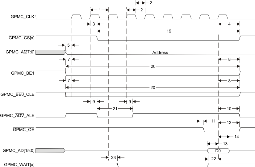 Figure 7-21 GPMC Nonmultiplexed NOR Flash - Synchronous Single Read (GPMCFCLKDIVIDER = 0)
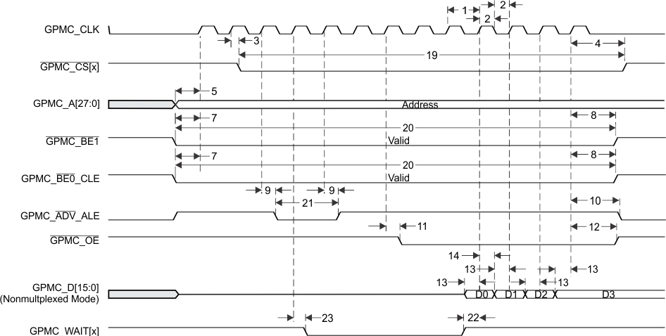 Figure 7-22 GPMC Nonmultiplexed NOR Flash - 14x16-bit Synchronous Burst Read (GPMCFCLKDIVIDER = 0)
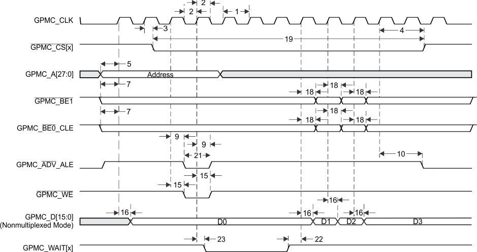 Figure 7-23 GPMC Nonmultiplexed NOR Flash - Synchronous Burst Write (GPMCFCLKDIVIDER = 0)
 Figure 7-24 GPMC Multiplexed NOR Flash - Synchronous Single Read (GPMCFCLKDIVIDER = 0)
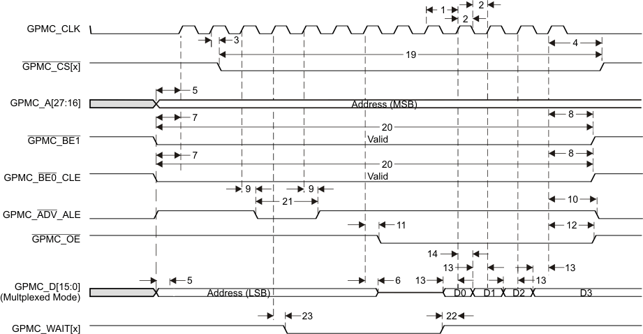 Figure 7-25 GPMC Multiplexed NOR Flash - 14x16-bit Synchronous Burst Read (GPMCFCLKDIVIDER = 0)
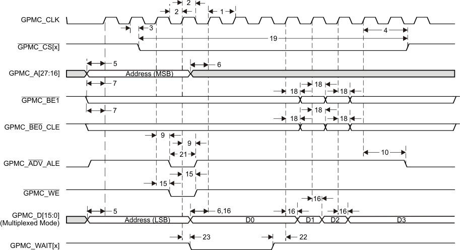 Figure 7-26 GPMC Nonmultiplexed NOR Flash - Synchronous Burst Write (GPMCFCLKDIVIDER = 0)
7.8.2.2 GPMC/NOR Flash Interface Asynchronous Mode Timing (Nonmultiplexed and Multiplexed Modes)
Table 7-36 Timing Requirements for GPMC/NOR Flash Interface - Asynchronous Mode(1)
(see Figure 7-27, Figure 7-28 for Nonmultiplexed Mode )(see Figure 7-29, Figure 7-31 for Multiplexed Mode)
| NO. | OPP100/120/166 | UNIT | |||
|---|---|---|---|---|---|
| MIN | MAX | ||||
| 6 | tacc(DAT) | Data maximum access time (GPMC_FCLK cycles) | H(2) | cycles | |
| 21 | tacc1-pgmode(DAT) | Page mode successive data maximum access time (GPMC_FCLK cycles) | P(3) | cycles | |
| 22 | tacc2-pgmode(DAT) | Page mode first data maximum access time (GPMC_FCLK cycles) | H(2) | cycles | |
Table 7-37 Switching Characteristics Over Recommended Operating Conditions for GPMC/NOR Flash Interface - Asynchronous Mode
(see Figure 7-27, Figure 7-28, Figure 7-29, Figure 7-30 for Nonmultiplexed Modes)(see Figure 7-31, Figure 7-32 for Multiplexed Modes)
| NO. | PARAMETER | OPP100/120/166 | UNIT | |||
|---|---|---|---|---|---|---|
| MIN | MAX | |||||
| 1 | tw(nBEV) | Pulse duration, GPMC_BE0_CLE, GPMC_BE1 valid time | N(1) | ns | ||
| 2 | tw(nCSV) | Pulse duration, GPMC_CS[x] low | A(2) | ns | ||
| 4 | td(nCSV-nADVIV) | Delay time, GPMC_CS[x] valid to GPMC_NADV_ALE invalid | B - 2(3) | B + 4(3) | ns | |
| 5 | td(nCSV-nOEIV) | Delay time, GPMC_CS[x] valid to GPMC_OE_RE invalid (single read) | C - 2(4) | C + 4(4) | ns | |
| 10 | td(AV-nCSV) | Delay time, GPMC_A[27:0] address bus valid to GPMC_CS[x] valid | MUX0 and Nonmulti Muxed pins | J - 2(5) | J + 4(5) | ns |
| MUX1 for GPMC_A[15:0] | J - 2(5) | J + 4(5) | ||||
| MUX1/2 for GPMC_A[27:20] | J - 2(5) | J + 4(5) | ||||
| 11 | td(nBEV-nCSV) | Delay time, GPMC_BE0_CLE, GPMC_BE1 valid to GPMC_CS[x] valid | J - 2(5) | J + 4(5) | ns | |
| 13 | td(nCSV-nADVV) | Delay time, GPMC_CS[x] valid to GPMC_ADV_ALE valid | K - 2(6) | K + 4(6) | ns | |
| 14 | td(nCSV-nOEV) | Delay time, GPMC_CS[x] valid to GPMC_OE_RE valid | L - 2(7) | L + 4(7) | ns | |
| 17 | tw(AIV) | Pulse duration, GPMC_A[27:0] address bus invalid between 2 successive R/W accesses | MUX0 and Nonmulti Muxed pins | G(8) | ns | |
| MUX1 for GPMC_A[15:0] | G(8) | |||||
| MUX1/2 for GPMC_A[27:20] | G(8) | |||||
| GPMC_D[15:0] | G(8) | |||||
| 19 | td(nCSV-nOEIV) | Delay time, GPMC_CS[x] valid to GPMC_OE_RE invalid (burst read) | I - 2(9) | I + 4(9) | ns | |
| 21 | tw(AV) | Pulse duration, GPMC_A[27:0] address bus valid: second, third and fourth accesses | MUX0 and Nonmulti Muxed pins | D(10) | ns | |
| MUX1 for GPMC_A[15:0] | D(10) | |||||
| MUX1/2 for GPMC_A[27:20] | D(10) | |||||
| GPMC_D[15:0] | D(10) | |||||
| 26 | td(nCSV-nWEV) | Delay time, GPMC_CS[x] valid to GPMC_WE valid | E - 2(11) | E + 4(11) | ns | |
| 28 | td(nCSV-nWEIV) | Delay time, GPMC_CS[x] valid to GPMC_WE invalid | F - 2(12) | F + 4(12) | ns | |
| 29 | td(nWEV-DV) | Delay time, GPMC_WE valid to GPMC_D[15:0] data bus valid | 2.0 | ns | ||
| 30 | td(DV-nCSV) | Delay time, GPMC_D[15:0] data bus valid to GPMC_CS[x] valid | J - 2(5) | J + 4(5) | ns | |
| 37 | td(ADVV-AIV) | Delay time, GPMC_ADV_ALE valid to GPMC_D[15:0] address invalid | MUX0 and Nonmulti Muxed pins | 2.0 | ns | |
| 38 | td(nOEV-AIV) | Delay time, GPMC_OE_RE valid to GPMC_D[15:0] address/data busses phase end | MUX0 and Nonmulti Muxed pins | 2.0 | ns | |
| MUX1 for GPMC_A[15:0] | 2.0 | |||||
| MUX1/2 for GPMC_A[27:20] | 2.0 | |||||
| GPMC_D[15:0] | 2.0 | |||||
| 39 | td(AIV-ADVV) | Delay time, GPMC_D[15:0] address valid to GPMC_ADV_ALE invalid | MUX0 and Nonmulti Muxed pins | 2.0 | ns | |
For single write: N = WrCycleTime * (TimeParaGranularity + 1) * GPMC_FCLK
For burst read: N = (RdCycleTime + (n - 1) * PageBurstAccessTime) * (TimeParaGranularity + 1) * GPMC_FCLK
For burst write: N = (WrCycleTime + (n - 1) * PageBurstAccessTime) * (TimeParaGranularity + 1) * GPMC_FCLK
For single write: A = (CSWrOffTime - CSOnTime) * (TimeParaGranularity + 1) * GPMC_FCLK
For burst read: A = (CSRdOffTime - CSOnTime + (n - 1) * PageBurstAccessTime) * (TimeParaGranularity + 1) * GPMC_FCLK
For burst write: A = (CSWrOffTime - CSOnTime + (n - 1) * PageBurstAccessTime) * (TimeParaGranularity + 1) * GPMC_FCLK
For reading: B = ((ADVRdOffTime - CSOnTime) * (TimeParaGranularity + 1) + 0.5 * (ADVExtraDelay - CSExtraDelay)) * GPMC_FCLK
For writing: B = ((ADVWrOffTime - CSOnTime) * (TimeParaGranularity + 1) + 0.5 * (ADVExtraDelay - CSExtraDelay)) * GPMC_FCLK
C = ((OEOffTime - CSOnTime) * (TimeParaGranularity + 1) + 0.5 * (OEExtraDelay - CSExtraDelay)) * GPMC_FCLK
J = (CSOnTime * (TimeParaGranularity + 1) + 0.5 * CSExtraDelay) * GPMC_FCLK
K = ((ADVOnTime - CSOnTime) * (TimeParaGranularity + 1) + 0.5 * (ADVExtraDelay - CSExtraDelay)) * GPMC_FCLK
L = ((OEOnTime - CSOnTime) * (TimeParaGranularity + 1) + 0.5 * (OEExtraDelay - CSExtraDelay)) * GPMC_FCLK
I = ((OEOffTime + (n - 1) * PageBurstAccessTime - CSOnTime) * (TimeParaGranularity + 1) + 0.5 * (OEExtraDelay - CSExtraDelay)) * GPMC_FCLK
E = ((WEOnTime - CSOnTime) * (TimeParaGranularity + 1) + 0.5 * (WEExtraDelay - CSExtraDelay)) * GPMC_FCLK
F = ((WEOffTime - CSOnTime) * (TimeParaGranularity + 1) + 0.5 * (WEExtraDelay - CSExtraDelay)) * GPMC_FCLK
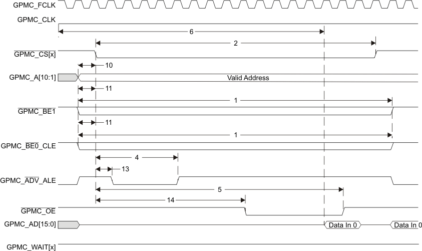 Figure 7-27 GPMC/Nonmultiplexed NOR Flash - Asynchronous Read - Single Word Timing
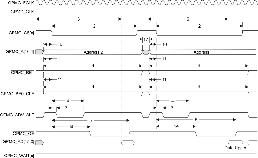 Figure 7-28 GPMC/Nonmultiplexed NOR Flash - Asynchronous Read - 32-Bit Access Timing
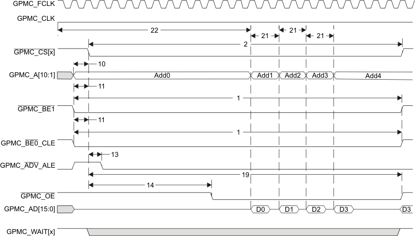 Figure 7-29 GPMC/Nonmultiplexed Only NOR Flash - Asynchronous Read - Page Mode 4x16-Bit Timing
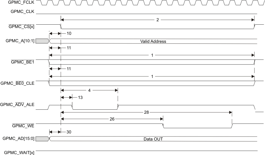 Figure 7-30 GPMC/Nonmultiplexed NOR Flash - Asynchronous Write - Single Word Timing
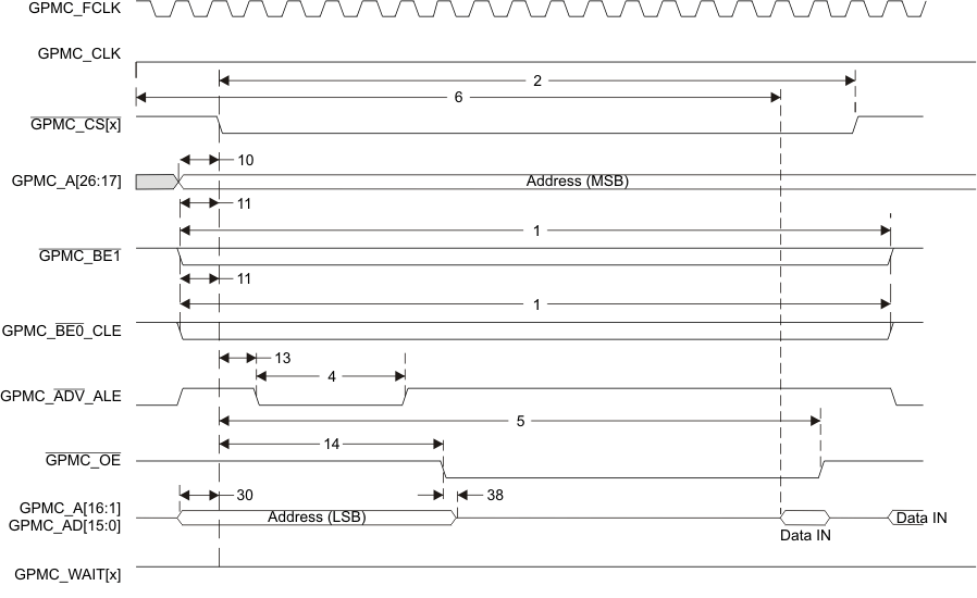 Figure 7-31 GPMC/Multiplexed NOR Flash - Asynchronous Read - Single Word Timing
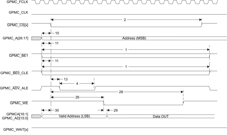 Figure 7-32 GPMC/Multiplexed NOR Flash - Asynchronous Write - Single Word Timing
7.8.2.3 GPMC/NAND Flash and ELM Interface Timing
Table 7-38 Timing Requirements for GPMC/NAND Flash Interface
(see Figure 7-35)| NO. | OPP100/120/166 | UNIT | |||
|---|---|---|---|---|---|
| MIN | MAX | ||||
| 13 | tacc(DAT) | Data maximum access time (GPMC_FCLK cycles) | J(1) | cycles | |
Table 7-39 Switching Characteristics Over Recommended Operating Conditions for GPMC/NAND Flash Interface
(see Figure 7-33, Figure 7-34, Figure 7-35, Figure 7-36)| NO. | PARAMETER | OPP100/120/166 | UNIT | ||
|---|---|---|---|---|---|
| MIN | MAX | ||||
| 1 | tw(nWEV) | Pulse duration, GPMC_WE valid time | A(1) | ns | |
| 2 | td(nCSV-nWEV) | Delay time, GPMC_CS[X] valid to GPMC_WE valid | B - 2(2) | B + 4(2) | ns |
| 3 | td(CLEH-nWEV) | Delay time, GPMC_BE0_CLE high to GPMC_WE valid | C - 2(3) | C + 4(3) | ns |
| 4 | td(nWEV-DV) | Delay time, GPMC_D[15:0] valid to GPMC_WE valid | D - 2(4) | D + 4(4) | ns |
| 5 | td(nWEIV-DIV) | Delay time, GPMC_WE invalid to GPMC_AD[15:0] invalid | E - 2(5) | E + 4(5) | ns |
| 6 | td(nWEIV-CLEIV) | Delay time, GPMC_WE invalid to GPMC_BE0_CLE invalid | F - 2(6) | F + 4(6) | ns |
| 7 | td(nWEIV-nCSIV) | Delay time, GPMC_WE invalid to GPMC_CS[X] invalid | G - 2(7) | G + 4(7) | ns |
| 8 | td(ALEH-nWEV) | Delay time, GPMC_ADV_ALE High to GPMC_WE valid | C - 2(3) | C + 4(3) | ns |
| 9 | td(nWEIV-ALEIV) | Delay time, GPMC_WE invalid to GPMC_ADV_ALE invalid | F - 2(6) | F + 4(6) | ns |
| 10 | tc(nWE) | Cycle time, write cycle time | H(8) | ns | |
| 11 | td(nCSV-nOEV) | Delay time, GPMC_CS[X] valid to GPMC_OE_RE valid | I - 2(9) | I + 4(9) | ns |
| 12 | tw(nOEV) | Pulse duration, GPMC_OE_RE valid time | K(10) | ns | |
| 13 | tc(nOE) | Cycle time, read cycle time | L(11) | ns | |
| 14 | td(nOEIV-nCSIV) | Delay time, GPMC_OE_RE invalid to GPMC_CS[X] invalid | M - 2(12) | M + 4(12) | ns |
B = ((WEOnTime - CSOnTime) * (TimeParaGranularity + 1) + 0.5 * (WEExtraDelay - CSExtraDelay)) * GPMC_FCLK
C = ((WEOnTime - ADVOnTime) * (TimeParaGranularity + 1) + 0.5 * (WEExtraDelay - ADVExtraDelay)) * GPMC_FCLK
D = (WEOnTime * (TimeParaGranularity + 1) + 0.5 * WEExtraDelay ) * GPMC_FCLK
E = ((WrCycleTime - WEOffTime) * (TimeParaGranularity + 1) - 0.5 * WEExtraDelay ) * GPMC_FCLK
F = ((ADVWrOffTime - WEOffTime) * (TimeParaGranularity + 1) + 0.5 * (ADVExtraDelay - WEExtraDelay )) * GPMC_FCLK
G = ((CSWrOffTime - WEOffTime) * (TimeParaGranularity + 1) + 0.5 * (CSExtraDelay - WEExtraDelay )) * GPMC_FCLK
I = ((OEOnTime - CSOnTime) * (TimeParaGranularity + 1) + 0.5 * (OEExtraDelay - CSExtraDelay)) * GPMC_FCLK
M = ((CSRdOffTime - OEOffTime) * (TimeParaGranularity + 1) + 0.5 * (CSExtraDelay - OEExtraDelay ))* GPMC_FCLK
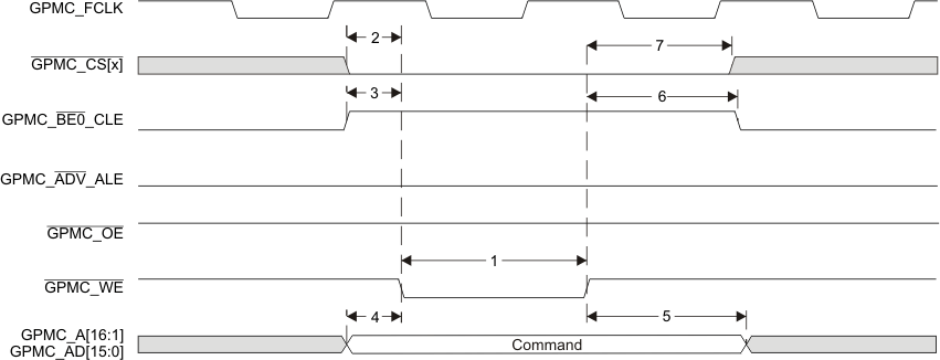 Figure 7-33 GPMC/NAND Flash - Command Latch Cycle Timing
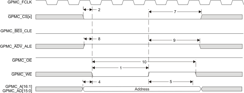 Figure 7-34 GPMC/NAND Flash - Address Latch Cycle Timing
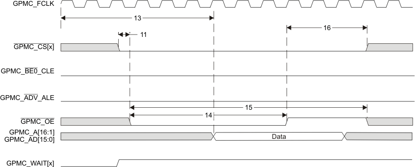 Figure 7-35 GPMC/NAND Flash - Data Read Cycle Timing
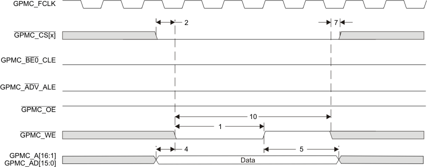 Figure 7-36 GPMC/NAND Flash - Data Write Cycle Timing
7.9 High-Definition Multimedia Interface (HDMI)
The device includes an HDMI 1.3a-compliant transmitter for digital video and audio data to display devices. The HDMI interface consists of a digital HDMI transmitter core with TMDS encoder, a core wrapper with interface logic and control registers, and a transmit PHY, with the following features:
- Hot-plug detection
- Consumer electronics control (CEC) messages
- DVI 1.0 compliant (only RGB pixel format)
- CEA 861-D and VESA DMT formats
- Supports up to 165-MHz pixel clock
- 1920 x 1080p @75 Hz with 8-bit/component color depth
- 1600 x 1200 @60 Hz with 8-bit/component color depth
- Support for deep-color mode:
- 10-bit/component color depth up to 1080p @60 Hz (Max pixel clock = 148.5 MHz)
- 12-bit/component color depth up to 720p/1080i @60 Hz (Max pixel clock = 123.75 MHz)
- TMDS clock to the HDMI-PHY is up to 185.625 MHz
- Maximum supported pixel clock:
- 165 MHz for 8-bit color depth
- 148.5 MHz for 10-bit color depth
- 123.75 MHz for 12-bit color depth
- Uncompressed multichannel (up to eight channels) audio (L-PCM) support
- Master I2C interface for display data channel (DDC) connection
For more details on the HDMI, see the High-Definition Multimedia Interface (HDMI) chapter of the AM387x Sitara™ ARM Processors Technical Reference Manual (Literature Number: SPRUGZ7).
7.9.1 HDMI Design Guidelines
This section provides PCB design and layout guidelines for the HDMI interface. The design rules constrain PCB trace length, PCB trace skew, signal integrity, cross-talk, and signal timing. Simulation and system design work has been done to ensure the HDMI interface requirements are met.
7.9.1.1 HDMI Interface Schematic
The HDMI bus is separated into three main sections:
- Transition Minimized Differential Signaling (TMDS) high-speed digital video interface
- Display Data Channel (I2C bus for configuration and status exchange between two devices)
- Consumer Electronics Control (optional) for remote control of connected devices.
The DDC and CEC are low-speed interfaces, so nothing special is required for PCB layout of these signals. Their connection is shown in Figure 7-37, HDMI Interface High-Level Schematic.
The TMDS channels are high-speed differential pairs and, therefore, require the most care in layout. Specifications for TMDS layout are below.
Figure 7-37 shows the HDMI interface schematic. The specific pin numbers can be obtained from Table 2-15, HDMI Terminal Functions.
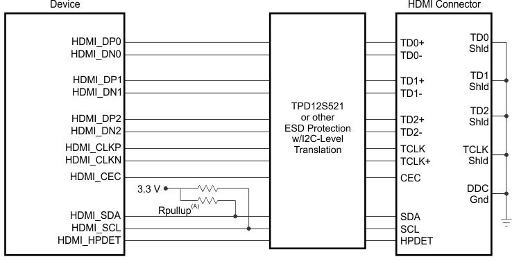
7.9.1.2 TMDS Routing
The TMDS signals are high-speed differential pairs. Care must be taken in the PCB layout of these signals to ensure good signal integrity.
The TMDS differential signal traces must be routed to achieve 100 Ω (±10%) differential impedance and 60 Ω (±10%) single-ended impedance. Single-ended impedance control is required because differential signals are extremely difficult to closely couple on PCBs and, therefore, single-ended impedance becomes important.
These impedances are impacted by trace width, trace spacing, distance to reference planes, and dielectric material. Verify with a PCB design tool that the trace geometry for both data signal pairs results in as close to 60 Ω impedance traces as possible. For best accuracy, work with your PCB fabricator to ensure this impedance is met.
In general, closely coupled differential signal traces are not an advantage on PCBs. When differential signals are closely coupled, tight spacing and width control is necessary. Very small width and spacing variations affect impedance dramatically, so tight impedance control can be more problematic to maintain in production.
Loosely coupled PCB differential signals make impedance control much easier. Wider traces and spacing make obstacle avoidance easier, and trace width variations do not affect impedance as much; therefore, it is easier to maintain an accurate impedance over the length of the signal. The wider traces also show reduced skin effect and, therefore, often result in better signal integrity.
Table 7-40 shows the routing specifications for the TMDS signals.
Table 7-40 TMDS Routing Specifications
| PARAMETER | MIN | TYP | MAX | UNIT |
|---|---|---|---|---|
| MPU-to-HDMI header trace length | 7000 | Mils | ||
| Number of stubs allowed on TMDS traces | 0 | Stubs | ||
| TX/RX pair differential impedance | 90 | 100 | 110 | Ω |
| TX/RX single ended impedance | 54 | 60 | 66 | Ω |
| Number of vias on each TMDS trace | 2 | Vias(1) | ||
| TMDS differential pair to any other trace spacing | 2*DS(2) |
7.9.1.3 DDC Signals
As shown in Figure 7-37, HDMI Interface High-Level Schematic, the DDC connects just like a standard I2C bus. As such, resistor pullups must be used to pull up the open drain buffer signals unless they are integrated into the ESD protection chip used. If used, these pullup resistors should be connected to a 3.3-V supply.
7.9.1.4 HDMI ESD Protection Device (Required)
Interfaces that connect to a cable such as HDMI generally require more ESD protection than can be built into the outputs of the processor. Therefore, this HDMI interface requires the use of an ESD protection chip to provide adequate ESD protection and to translate I2C voltage levels from the 3.3 V supplied by the device to the 5 volts required by the HDMI specification.
When selecting an ESD protection chip, choose the lowest capacitance ESD protection available to minimize signal degradation. In no case should the ESD protection circuit capacitance be more than 5 pF.
TI manufactures devices that provide ESD protection for HDMI signals such as the TPD12S521. For more information see the www.ti.com website.
7.9.1.5 PCB Stackup Specifications
Table 7-41 shows the stackup and feature sizes required for HDMI.
Table 7-41 HDMI PCB Stackup Specifications
| PARAMETER | MIN | TYP | MAX | UNIT |
|---|---|---|---|---|
| PCB routing/plane layers | 4 | 6 | - | Layers |
| Signal routing layers | 2 | 3 | - | Layers |
| Number of ground plane cuts allowed within HDMI routing region | - | - | 0 | Cuts |
| Number of layers between HDMI routing region and reference ground plane | - | - | 0 | Layers |
| PCB trace width | - | 4 | - | Mils |
| PCB BGA escape via pad size | - | 20 | - | Mils |
| PCB BGA escape via hole size | - | 10 | Mils | |
| MPU device BGA pad size(1)(2) | 0.4 | mm |
7.9.1.6 Grounding
Each TMDS channel has its own shield pin which should be grounded to provide a return current path for the TMDS signal.
7.10 High-Definition Video Processing Subsystem (HDVPSS)
The device High-Definition Video Processing Subsystem (HDVPSS) provides a video input interface for external imaging peripherals (that is, image sensors, video decoders, and so on) and a video output interface for display devices, such as analog SDTV displays, digital HDTV displays, digital LCD panels, and so on. The HDVPSS includes HD and SD video encoders and an HDMI transmitter interface.
The device HDVPSS features include:
- Two display processing pipelines with de-interlacing, scaling, alpha blending, chroma keying, color space conversion, flicker filtering, and pixel format conversion.
- HD/SD compositor features for PIP support.
- Format conversions (up to 1080p 60 Hz) include scan format conversion, scan rate conversion, aspect-ratio conversion, and frame size conversion.
- Supports additional video processing capabilities by using the memory-to-memory feature of the subsystem.
- Two parallel video processing pipelines support HD (up to 1080p60) and SD (NTSC/PAL) simultaneous outputs.
- SD analog output with OSD with embedded timing codes (BT.656)
- S-video or Composite output
- 2-channel SD-DAC with 10-bit resolution
- Options available to support MacroVision and CGMS-A (contact local TI Sales rep for information).
- Digital HDMI 1.3a-compliant transmitter (for details, see Section 7.9, High-Definition Multimedia Interface (HDMI)).
- One digital video output supporting up to 30-bits @ 165 MHz
- One digital video output supporting up to 24-bits @ 165 MHz
- SD analog output with OSD with embedded timing codes (BT.656)
- Two independently configurable external video input capture ports (up to 165 MHz).
- 16/24-bit HD digital video input or dual clock independent 8-bit SD inputs on each capture port.
- 8/16/24-bit digital video input
- 8-bit digital video input
- Embedded sync and external sync modes are supported for all input configurations (VIN1 Port B supports embedded sync only).
- Demultiplexing of both pixel-to-pixel and line-to-line multiplexed streams, effectively supporting up to 16 simultaneous SD inputs with a glueless interface to an external multiplexer such as the TVP5158.
- Additional features include: programmable color space conversion, scaler and chroma downsampler, ancillary VANC/VBI data capture (decoded by software).
- Graphics features:
- Three independently-generated graphics layers.
- Each supports full-screen resolution graphics in HD, SD or both.
- Up/down scaler optimized for graphics.
- Global and pixel-level alpha blending supported.
For more detailed information on specific features and registers, see the High Definition Video Processing Subsystem chapter of the AM387x Sitara™ ARM Processors Technical Reference Manual (Literature Number: SPRUGZ7).
7.10.1 HDVPSS Electrical Data/Timing
Table 7-42 Timing Requirements for HDVPSS Input
(see Figure 7-38 and Figure 7-39)| NO. | OPP100/120/166 | UNIT | |||
|---|---|---|---|---|---|
| MIN | MAX | ||||
| VIN[X]A_CLK | |||||
| 1 | tc(CLK) | Cycle time, VIN[x]A_CLK | 6.06(1) | ns | |
| 2 | tw(CLKH) | Pulse duration, VIN[x]A_CLK high (45% of tc) | 2.73 | ns | |
| 3 | tw(CLKH) | Pulse duration, VIN[x]A_CLK low (45% of tc) | 2.73 | ns | |
| 4 | tsu(DE-CLK) | Input setup time, control valid to VIN[x]A_CLK high/low | 3 | ns | |
| tsu(VSYNC-CLK) | |||||
| tsu(FLD-CLK) | |||||
| tsu(HSYNC-CLK) | |||||
| tsu(D-CLK) | Input setup time, data valid to VIN[x]A_CLK high/low | 3 | |||
| 5 | th(CLK-DE) | Input hold time, control valid from VIN[x]A_CLK high/low | 0.1 | ns | |
| th(CLK-VSYNC) | |||||
| th(CLK-FLD) | |||||
| th(CLK-HSYNC) | |||||
| th(CLK-D) | Input hold time, data valid from VIN[x]A_CLK high/low | 0.1 | |||
| VIN[x]B_CLK | |||||
| 1 | tc(CLK) | Cycle time, VIN[x]B_CLK | 6.06(1) | ns | |
| 2 | tw(CLKH) | Pulse duration, VIN[x]B_CLK high (45% of tc) | 2.73 | ns | |
| 3 | tw(CLKH) | Pulse duration, VIN[x]B_CLK low (45% of tc) | 2.73 | ns | |
| 4 | tsu(DE-CLK) | Input setup time, control valid to VIN[x]B_CLK high/low | 3 | ns | |
| tsu(VSYNC-CLK) | |||||
| tsu(FLD-CLK) | |||||
| tsu(HSYNC-CLK) | |||||
| tsu(D-CLK) | Input setup time, data valid to VIN[x]B_CLK high/low | 3 | |||
| 5 | th(CLK-DE) | Input hold time, control valid from VIN[x]B_CLK high/low | 0.1 | ns | |
| th(CLK-VSYNC) | |||||
| th(CLK-FLD) | |||||
| th(CLK-HSYNC) | |||||
| th(CLK-D) | Input hold time, data valid from VIN[x]B_CLK high/low | 0.1 | |||
Table 7-43 Switching Characteristics Over Recommended Operating Conditions for HDVPSS Output
(see Figure 7-38 and Figure 7-40)| NO. | PARAMETER | OPP100/120/166 | UNIT | ||
|---|---|---|---|---|---|
| MIN | MAX | ||||
| 1 | tc(CLK) | Cycle time, VOUT[x]_CLK | 6.06(1) | ns | |
| 2 | tw(CLKH) | Pulse duration, VOUT[x]_CLK high (45% of tc) | 2.73 | ns | |
| 3 | tw(CLKL) | Pulse duration, VOUT[x]_CLK low (45% of tc) | 2.73 | ns | |
| 7 | tt(CLK) | Transition time, VOUT[x]_CLK (10%-90%) | 2.64 | ns | |
| 6 | td(CLK-AVID) | Delay time, VOUT[x]_CLK low (falling) to control valid | -1.2 | 2 | ns |
| td(CLK-FLD) | |||||
| td(CLK-VSYNC) | |||||
| td(CLK-HSYNC) | |||||
| td(CLK-RCR) | Delay time, VOUT[0]_CLK low (falling) to data valid | -1.2 | 2 | ns | |
| td(CLK-GYYC) | |||||
| td(CLK-BCBC) | |||||
| td(CLK-YYC) | Delay time, VOUT[1]_CLK low (falling) to data valid | ||||
| td(CLK-C) | |||||
 Figure 7-38 HDVPSS Clock Timing
 Figure 7-39 HDVPSS Input Timing
 Figure 7-40 HDVPSS Output Timing
7.10.2 Video DAC Guidelines and Electrical Data/Timing
The analog video DAC outputs of the device can be operated in one of two modes: Normal mode and TVOUT Bypass mode. In Normal mode, the device’s internal video amplifier is used. In TVOUT Bypass mode, the internal video amplifier is bypassed and an external amplifier is required.
Figure 7-41 shows a typical circuit that permits connecting the analog video output from the device to standard 75-Ω impedance video systems in Normal mode. Figure 7-42 shows a typical circuit that permits connecting the analog video output from the device to standard 75-Ω impedance video systems in TVOUT Bypass mode.
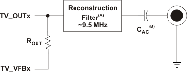

During board design, the onboard traces and parasitics must be matched for the channel. The video DAC output pins (TV_OUTx/TV_VFBx) are very high-frequency analog signals and must be routed with extreme care. As a result, the paths of these signals must be as short as possible, and as isolated as possible from other interfering signals. In TVOUT Bypass mode, the load resistor and amplifier/buffer should be placed as close as possible to the TV_VFBx pins. Other layout guidelines include:
- Take special care to bypass the VDDA_VDAC_1P8 power supply pin with a capacitor. For more information, see Section 6.2.9, Power-Supply Decoupling.
- In TVOUT Bypass mode, place the RLOAD resistor as close as possible to the Reconstruction Filter and Amplifier. In addition, place the 75-Ω resistor as close as possible (< 0.5 ") to the Amplifier/buffer output pin. To maintain a high-quality video signal, the onboard traces after the 75-Ω resistor should have a characteristic impedance of 75 Ω (± 20%).
- In Normal mode, TV_VFBx is the most sensitive pin in the TV out system. The ROUT resistor should be placed as close as possible to the device pins. To maintain a high-quality video signal, the onboard traces leading to the TV_OUTx pin should have a characteristic impedance of 75 Ω (± 20%) starting from the closest possible place to the device pin output.
- Minimize input trace lengths to the device to reduce parasitic capacitance.
- Include solid ground return paths.
- Match trace lengths as close as possible within a video format group (that is, Y and C for S-Video output should match each other).
For additional Video DAC Design guidelines, see the High Definition Video Processing Subsystem chapter of the AM387x Sitara™ ARM Processors Technical Reference Manual (Literature Number: SPRUGZ7).
Table 7-44 Static and Dynamic DAC Specifications
| VDAC STATIC SPECIFICATIONS | |||||
|---|---|---|---|---|---|
| PARAMETER | TEST CONDITIONS | MIN | TYP | MAX | UNIT |
| Reference Current Setting Resistor (RSET) | Normal Mode | 4653 | 4700 | 4747 | Ω |
| TVOUT Bypass Mode | 9900 | 10000 | 10100 | Ω | |
| Output resistor between TV_OUTx and TV_VFBx pins (ROUT) | Normal Mode | 2673 | 2700 | 2727 | Ω |
| TVOUT Bypass Mode | N/A | ||||
| Load Resistor (RLOAD) | Normal Mode | 75-Ω Inside the Display | |||
| TVOUT Bypass Mode | 1485 | 1500 | 1515 | Ω | |
| AC-Coupling Capacitor (Optional) [CAC] | Normal Mode | 220 | uF | ||
| TVOUT Bypass Mode | See External Amplifier Specification | ||||
| Total Capacitance from TV_OUTx to VSSA_VDAC_1P8 | Normal Mode | 300 | pF | ||
| TVOUT Bypass Mode | N/A | ||||
| Resolution | 10 | Bits | |||
| Integral Nonlinearity (INL), Best Fit | Normal Mode | -4 | 4 | LSB | |
| TVOUT Bypass Mode | -1 | 1 | LSB | ||
| Differential Nonlinearity (DNL) | Normal Mode | -2.5 | 2.5 | LSB | |
| TVOUT Bypass Mode | -1 | 1 | LSB | ||
| Full-Scale Output Voltage | Normal Mode (RLOAD = 75 Ω) | 1.3 | V | ||
| TVOUT Bypass Mode (RLOAD = 1.5 kΩ) | 0.7 | V | |||
| Full-Scale Output Current | Normal Mode | N/A | |||
| TVOUT Bypass Mode | 470 | uA | |||
| Gain Error | Normal Mode (Composite) and TVOUT Bypass Mode | -10 | 10 | %FS | |
| Normal Mode (S-Video) | -20 | 20 | %FS | ||
| Gain Mismatch (Luma-to-Chroma) | Normal Mode (Composite) | N/A | |||
| Normal Mode (S-Video) | -10 | 10 | % | ||
| Output Impedance | Looking into TV_OUTx nodes | 75 | Ω | ||
| VDAC DYNAMIC SPECIFICATIONS | |||||
| PARAMETER | TEST CONDITIONS | MIN | TYP | MAX | UNIT |
| Output Update Rate (FCLK) | 54 | 60 | MHz | ||
| Signal Bandwidth | 3 dB | 6 | MHz | ||
| Spurious-Free Dynamic Range (SFDR) within bandwidth | FCLK = 54 MHz, FOUT = 1 MHz | 50 | dBc | ||
| Signal-to-Noise Ration (SNR) | FCLK = 54 MHz, FOUT = 1 MHz | 54 | dB | ||
| Power Supply Rejection (PSR) | Normal Mode, 100 mVpp @ 6 MHz on VDDA_VDAC_1P8 | 6 | dB | ||
| TVOUT Bypass Mode, 100 mVpp @ 6 MHz on VDDA_VDAC_1P8 | 20 | ||||
7.11 Inter-Integrated Circuit (I2C)
The device includes four inter-integrated circuit (I2C) modules which provide an interface to other devices compliant with Philips Semiconductors Inter-IC bus (I2C-bus™) specification version 2.1. External components attached to this 2-wire serial bus can transmit/receive 8-bit data to/from the device through the I2C module. The I2C port does not support CBUS compatible devices.
The I2C port supports the following features:
- Compatible with Philips I2C Specification Revision 2.1 (January 2000)
- Standard and fast modes from 10 - 400 Kbps (no fail-safe I/O buffers)
- Noise filter to remove noise 50 ns or less
- Seven- and ten-bit device addressing modes
- Multimaster transmitter/slave receiver mode
- Multimaster receiver/slave transmitter mode
- Combined master transmit/receive and receive/transmit modes
- Two DMA channels, one interrupt line
- Built-in FIFO (32 byte) for buffered read or write.
For more detailed information on the I2C peripheral, see the Inter-Integrated Circuit (I2C) Controller Module chapter of the AM387x Sitara™ ARM Processors Technical Reference Manual (Literature Number: SPRUGZ7).
7.11.1 I2C Peripheral Register Descriptions
Table 7-45 I2C Registers
| HEX ADDRESS | |||||
|---|---|---|---|---|---|
| I2C0 | I2C1 | I2C2 | I2C3 | ACRONYM | REGISTER NAME |
| 0x4802 8000 | 0x4802 A000 | 0x4819 C000 | 0x4819 E000 | I2C_REVNB_LO | Module Revision (LOW BYTES) |
| 0x4802 8004 | 0x4802 A004 | 0x4819 C004 | 0x4819 E004 | I2C_REVNB_HI | Module Revision (HIGH BYTES) |
| 0x4802 8010 | 0x4802 A010 | 0x4819 C010 | 0x4819 E010 | I2C_SYSC | System configuration |
| 0x4802 8020 | 0x4802 A020 | 0x4819 C020 | 0x4819 E020 | I2C_EOI | I2C End of Interrupt |
| 0x4802 8024 | 0x4802 A024 | 0x4819 C024 | 0x4819 E024 | I2C_IRQSTATUS_RAW | I2C Status Raw |
| 0x4802 8028 | 0x4802 A028 | 0x4819 C028 | 0x4819 E028 | I2C_IRQSTATUS | I2C Status |
| 0x4802 802C | 0x4802 A02C | 0x4819 C02C | 0x4819 E02C | I2C_IRQENABLE_SET | I2C Interrupt Enable Set |
| 0x4802 8030 | 0x4802 A030 | 0x4819 C030 | 0x4819 E030 | I2C_IRQENABLE_CLR | I2C Interrupt Enable Clear |
| 0x4802 8034 | 0x4802 A034 | 0x4819 C034 | 0x4819 E034 | I2C_WE | I2C Wakeup Enable |
| 0x4802 8038 | 0x4802 A038 | 0x4819 C038 | 0x4819 E038 | I2C_DMARXENABLE_SET | Receive DMA Enable Set |
| 0x4802 803C | 0x4802 A03C | 0x4819 C03C | 0x4819 E03C | I2C_DMATXENABLE_SET | Transmit DMA Enable Set |
| 0x4802 8040 | 0x4802 A040 | 0x4819 C040 | 0x4819 E040 | I2C_DMARXENABLE_CLR | Receive DMA Enable Clear |
| 0x4802 8044 | 0x4802 A044 | 0x4819 C044 | 0x4819 E044 | I2C_DMATXENABLE_CLR | Transmit DMA Enable Clear |
| 0x4802 8048 | 0x4802 A048 | 0x4819 C048 | 0x4819 E048 | I2C_DMARXWAKE_EN | Receive DMA Wakeup |
| 0x4802 804C | 0x4802 A04C | 0x4819 C04C | 0x4819 E04C | I2C_DMATXWAKE_EN | Transmit DMA Wakeup |
| 0x4802 8090 | 0x4802 A090 | 0x4819 C090 | 0x4819 E090 | I2C_SYSS | System Status |
| 0x4802 8094 | 0x4802 A094 | 0x4819 C094 | 0x4819 E094 | I2C_BUF | Buffer Configuration |
| 0x4802 8098 | 0x4802 A098 | 0x4819 C098 | 0x4819 E098 | I2C_CNT | Data Counter |
| 0x4802 809C | 0x4802 A09C | 0x4819 C09C | 0x4819 E09C | I2C_DATA | Data Access |
| 0x4802 80A4 | 0x4802 A0A4 | 0x4819 C0A4 | 0x4819 E0A4 | I2C_CON | I2C Configuration |
| 0x4802 80A8 | 0x4802 A0A8 | 0x4819 C0A8 | 0x4819 E0A8 | I2C_OA | I2C Own Address |
| 0x4802 80AC | 0x4802 A0AC | 0x4819 C0AC | 0x4819 E0AC | I2C_SA | I2C Slave Address |
| 0x4802 80B0 | 0x4802 A0B0 | 0x4819 C0B0 | 0x4819 E0B0 | I2C_PSC | I2C Clock Prescaler |
| 0x4802 80B4 | 0x4802 A0B4 | 0x4819 C0B4 | 0x4819 E0B4 | I2C_SCLL | I2C SCL Low Time |
| 0x4802 80B8 | 0x4802 A0B8 | 0x4819 C0B8 | 0x4819 E0B8 | I2C_SCLH | I2C SCL High Time |
| 0x4802 80BC | 0x4802 A0BC | 0x4819 C0BC | 0x4819 E0BC | I2C_SYSTEST | System Test |
| 0x4802 80C0 | 0x4802 A0C0 | 0x4819 C0C0 | 0x4819 E0C0 | I2C_BUFSTAT | I2C Buffer Status |
| 0x4802 80C4 | 0x4802 A0C4 | 0x4819 C0C4 | 0x4819 E0C4 | I2C_OA1 | I2C Own Address 1 |
| 0x4802 80C8 | 0x4802 A0C8 | 0x4819 C0C8 | 0x4819 E0C8 | I2C_OA2 | I2C Own Address 2 |
| 0x4802 80CC | 0x4802 A0CC | 0x4819 C0CC | 0x4819 E0CC | I2C_OA3 | I2C Own Address 3 |
| 0x4802 80D0 | 0x4802 A0D0 | 0x4819 C0D0 | 0x4819 E0D0 | I2C_ACTOA | Active Own Address |
| 0x4802 80D4 | 0x4802 A0D4 | 0x4819 C0D4 | 0x4819 E0D4 | I2C_SBLOCK | I2C Clock Blocking Enable |
7.11.2 I2C Electrical Data/Timing
Table 7-46 Timing Requirements for I2C Input Timings(1)
(see Figure 7-43)| NO. | OPP100/120/166 | UNIT | ||||||
|---|---|---|---|---|---|---|---|---|
| STANDARD MODE | FAST MODE | |||||||
| MIN | MAX | MIN | MAX | |||||
| 1 | tc(SCL) | Cycle time, SCL | 10 | 2.5 | µs | |||
| 2 | tsu(SCLH-SDAL) | Setup time, SCL high before SDA low (for a repeated START condition) | 4.7 | 0.6 | µs | |||
| 3 | th(SDAL-SCLL) | Hold time, SCL low after SDA low (for a START and a repeated START condition) | 4 | 0.6 | µs | |||
| 4 | tw(SCLL) | Pulse duration, SCL low | 4.7 | 1.3 | µs | |||
| 5 | tw(SCLH) | Pulse duration, SCL high | 4 | 0.6 | µs | |||
| 6 | tsu(SDAV-SCLH) | Setup time, SDA valid before SCL high | 250 | 100(2) | ns | |||
| 7 | th(SCLL-SDAV) | Hold time, SDA valid after SCL low | 0(3) | 3.45(4) | 0(3) | 0.9(4) | µs | |
| 8 | tw(SDAH) | Pulse duration, SDA high between STOP and START conditions | 4.7 | 1.3 | µs | |||
| 9 | tr(SDA) | Rise time, SDA | 1000 | 20 + 0.1Cb (5) | 300 | ns | ||
| 10 | tr(SCL) | Rise time, SCL | 1000 | 20 + 0.1Cb (5) | 300 | ns | ||
| 11 | tf(SDA) | Fall time, SDA | 300 | 20 + 0.1Cb (5) | 300 | ns | ||
| 12 | tf(SCL) | Fall time, SCL | 300 | 20 + 0.1Cb (5) | 300 | ns | ||
| 13 | tsu(SCLH-SDAH) | Setup time, SCL high before SDA high (for STOP condition) | 4 | 0.6 | µs | |||
| 14 | tw(SP) | Pulse duration, spike (must be suppressed) | 0 | 50 | ns | |||
| 15 | Cb (5) | Capacitive load for each bus line | 400 | 400 | pF | |||
 Figure 7-43 I2C Receive Timing
Table 7-47 Switching Characteristics Over Recommended Operating Conditions for I2C Output Timings
(see Figure 7-44)| NO. | PARAMETER | OPP100/120/166 | UNIT | |||||
|---|---|---|---|---|---|---|---|---|
| STANDARD MODE | FAST MODE | |||||||
| MIN | MAX | MIN | MAX | |||||
| 16 | tc(SCL) | Cycle time, SCL | 10 | 2.5 | µs | |||
| 17 | tsu(SCLH-SDAL) | Setup time, SCL high before SDA low (for a repeated START condition) | 4.7 | 0.6 | µs | |||
| 18 | th(SDAL-SCLL) | Hold time, SCL low after SDA low (for a START and a repeated START condition) | 4 | 0.6 | µs | |||
| 19 | tw(SCLL) | Pulse duration, SCL low | 4.7 | 1.3 | µs | |||
| 20 | tw(SCLH) | Pulse duration, SCL high | 4 | 0.6 | µs | |||
| 21 | tsu(SDAV-SCLH) | Setup time, SDA valid before SCL high | 250 | 100 | ns | |||
| 22 | th(SCLL-SDAV) | Hold time, SDA valid after SCL low (for I2C bus devices) | 0 | 3.45 | 0 | 0.9 | µs | |
| 23 | tw(SDAH) | Pulse duration, SDA high between STOP and START conditions | 4.7 | 1.3 | µs | |||
| 24 | tr(SDA) | Rise time, SDA | 1000 | 20 + 0.1Cb (1) | 300 | ns | ||
| 25 | tr(SCL) | Rise time, SCL | 1000 | 20 + 0.1Cb (1) | 300 | ns | ||
| 26 | tf(SDA) | Fall time, SDA | 300 | 20 + 0.1Cb (1) | 300 | ns | ||
| 27 | tf(SCL) | Fall time, SCL | 300 | 20 + 0.1Cb (1) | 300 | ns | ||
| 28 | tsu(SCLH-SDAH) | Setup time, SCL high before SDA high (for STOP condition) | 4 | 0.6 | µs | |||
| 29 | Cp | Capacitance for each I2C pin | 10 | 10 | pF | |||
 Figure 7-44 I2C Transmit Timing
7.12 Imaging Subsystem (ISS)
The device Imaging Subsystem captures and processes pixel data from external image and video inputs. The inputs can be connected to the Image Processing block through the Parallel Camera Interface (CAM). . In addition, a Timing control module provides flash strobe and mechanical shutter interfaces. The features of each component of the ISS are described below.
- Parallel Camera (CAM) interface features:
- Input format
- Bayer pattern Raw (up to 16bit) or YCbCr 422 (8bit or 16bit) data.
- ITU-R BT.656/1120 standard format
- Generates HD/VD timing signals and field ID to an external timing generator, or can synchronize to the external timing generator.
- Support for progressive and interlaced sensors (hardware support for up to 2 fields and firmware supports for higher number of fields, typically 3-, 4-, and 5-field sensors.
- Input format
- Image Sensor Interface (ISIF) features:
- Support for up to 32K pixels (image size) in both the horizontal and vertical direction
- Color space conversion for non-Bayer pattern Raw data
- Digital black clamping with Horizontal/Vertical offset drift compensation
- Vertical Line defect correction based on a lookup table
- Color-dependent gain control and black level offset control
- Ability to control output to the DDR2/DDR3 via an external write enable signal
- Down sampling via programmable culling patterns
- A-law/DPCM compression
- Generating 16-, 12- or 8-bit output to memory
- Two independent Resizers
- Providing two different sizes of outputs simultaneously on one input
- Maximum line width is 5376 and 2336, respectively
- YUV422 to YUV420 conversion
- Data output format: RGB565, ARGB888, YUV422 co sited and YUV4:2:0 planar
- Resizer Ratio: x1/4096 approximately x20
- Input from memory
- Timing control module features:
- STROBE signal for flash prestrobe and flash strobe
- SHUTTER signal for mechanical shutter control
- Global reset control
For more detailed information on the ISS, see the ISS Overview section, the ISS Interfaces section, and the ISS ISP section of the Watchdog Timer chapter of the AM387x Sitara™ ARM Processors Technical Reference Manual (Literature Number: SPRUGZ7).
7.12.1 ISSCAM Electrical Data/Timing
Table 7-48 Timing Requirements for ISSCAM (see Figure 7-45)
| NO. | OPP100/120/166 | UNIT | ||||
|---|---|---|---|---|---|---|
| MIN | NOM | MAX | ||||
| 1 | tc(PCLK) | Cycle time, PCLK | 6.06 | ns | ||
| 2 | tw(PCLKH) | Pulse duration, PCLK high | 2.73 | ns | ||
| 3 | tw(PCLKL) | Pulse duration, PCLK low | 2.73 | ns | ||
| 4 | tt(PCLK) | Transition time, PCLK | 2.64 | ns | ||
| 5 | tsu(DATA-PCLK) | Input setup time, Data/Control valid before PCLK high/low | 3.11 | ns | ||
| tsu(DE-PCLK) | 3.11 | ns | ||||
| tsu(VS-PCLK) | 3.11 | ns | ||||
| tsu(HS-PCLK) | 3.11 | ns | ||||
| tsu(FLD-PCLK) | 3.11 | ns | ||||
| 6 | th(PCLK-DATA) | Input hold time, Data/Control valid after PCLK high/low | -0.15 | ns | ||
| th(PCLK-DE) | -0.15 | ns | ||||
| th(PCLK-VS) | -0.15 | ns | ||||
| th(PCLK-HS) | -0.15 | ns | ||||
| th(PCLK-FLD) | -0.15 | ns | ||||
Table 7-49 Switching Characteristics Over Recommended Operating Conditions for ISSCAM (see Figure 7-45)
| NO. | PARAMETER | OPP100/120/166 | UNIT | |||
|---|---|---|---|---|---|---|
| MIN | MAX | |||||
| 15 | td(PCLK-FLD) | Delay time, PCLK rising/falling clock edge to Control valid | 3 | 11.5 | ns | |
| 16 | td(PCLK-VS) | Delay time, PCLK rising/falling clock edge to Control valid | 3 | 11.5 | ns | |
| 17 | td(PCLK-HS) | Delay time, PCLK rising/falling clock edge to Control valid | 3 | 11.5 | ns | |
| 18 | td(PCLK-STROBE) | Delay time, PCLK rising/falling clock edge to Control valid | 3 | 11.5 | ns | |
| 19 | td(PCLK-SHUTTER) | Delay time, PCLK rising/falling clock edge to Control valid | 3 | 11.5 | ns | |
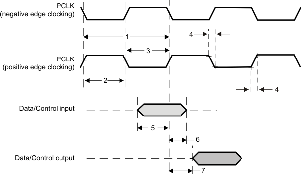 Figure 7-45 ISSCAM Timings
7.13 DDR2/DDR3 Memory Controller
The device has a dedicated interface to DDR3 and DDR2 SDRAM. The device dedicated interface also supports JEDEC standard compliant DDR2 and DDR3 SDRAM devices with the following features:
- 16-bit or 32-bit data path to external SDRAM memory
- Memory device capacity: 64Mb, 128Mb, 256Mb, 512Mb, 1Gb, 2Gb, and 4Gb devices
- Support for two independent chip selects, with their corresponding register sets, and independent page tracking
- Two interfaces with associated DDR2/DDR3 PHYs
- Dynamic memory manager allows for interleaving of data between the two DDR interfaces.
For details on the DDR2/DDR3 Memory Controller, see the DDR2/DDR3 Memory Controller chapter of the AM387x Sitara™ ARM Processors Technical Reference Manual (Literature Number: SPRUGZ7).
7.13.1 DDR2/3 Memory Controller Register Descriptions
Table 7-50 DDR2/3 Memory Controller Registers
| DDR0 HEX ADDRESS | DDR1 HEX ADDRESS | ACRONYM | REGISTER NAME |
|---|---|---|---|
| 0x4C00 0004 | 0x4D00 0004 | SDRSTAT | SDRAM Status Register |
| 0x4C00 0008 | 0x4D00 0008 | SDRCR | SDRAM Configuration Register |
| 0x4C00 000C | 0x4D00 000C | SDRCR2 | SDRAM Configuration Register 2 |
| 0x4C00 0010 | 0x4D00 0010 | SDRRCR | SDRAM Refresh Control Register |
| 0x4C00 0014 | 0x4D00 0014 | SDRRCSR | SDRAM Refresh Control Shadow Register |
| 0x4C00 0018 | 0x4D00 0018 | SDRTIM1 | SDRAM Timing 1 Register |
| 0x4C00 001C | 0x4D00 001C | SDRTIM1SR | SDRAM Timing 1 Shadow Register |
| 0x4C00 0020 | 0x4D00 0020 | SDRTIM2 | SDRAM Timing 2 Register |
| 0x4C00 0024 | 0x4D00 0024 | SDRTIM2SR | SDRAM Timing 2 Shadow Register |
| 0x4C00 0028 | 0x4D00 0028 | SDRTIM3 | SDRAM Timing 3 Register |
| 0x4C00 002C | 0x4D00 002C | SDRTIM3SR | SDRAM Timing 3 Shadow Register |
| 0x4C00 0038 | 0x4D00 0038 | PMCR | Power Management Control Register |
| 0x4C00 003C | 0x4D00 003C | PMCSR | Power Management Control Shadow Register |
| 0x4C00 0054 | 0x4D00 0054 | PBBPR | Peripheral Bus Burst Priority Register |
| 0x4C00 00A0 | 0x4D00 00A0 | EOI | End of Interrupt Register |
| 0x4C00 00A4 | 0x4D00 00A4 | SOIRSR | System OCP Interrupt Raw Status Register |
| 0x4C00 00AC | 0x4D00 00AC | SOISR | System OCP Interrupt Status Register |
| 0x4C00 00B4 | 0x4D00 00B4 | SOIESR | System OCP Interrupt Enable Set Register |
| 0x4C00 00BC | 0x4D00 00BC | SOIECR | System OCP Interrupt Enable Clear Register |
| 0x4C00 00C8 | 0x4D00 00C8 | ZQCR | SDRAM Output Impedance Calibration Configuration Register |
| 0x4C00 00D4 | 0x4D00 00D4 | RDWR_LVL_RMP_WIN | Read-Write Leveling Ramp Window Register |
| 0x4C00 00D8 | 0x4D00 00D8 | RDWR_LVL_RMP_CTRL | Read-Write Leveling Ramp Control Register |
| 0x4C00 00DC | 0x4D00 00DC | RWLCR | Read-Write Leveling Control Register |
| 0x4C00 00E4 | 0x4D00 00E4 | DDRPHYCR | DDR PHY Control Register |
| 0x4C00 00E8 | 0x4D00 00E8 | DDRPHYCSR | DDR PHY Control Shadow Register |
| 0x4C00 0100 | 0x4D00 0100 | PRI_COS_MAP | Priority to Class of Service Mapping Register |
| 0x4C00 0104 | 0x4D00 0104 | CONNID_COS_1_MAP | Connection ID to Class of Service 1 Mapping Register |
| 0x4C00 0108 | 0x4D00 0108 | CONNID_COS_2_MAP | Connection ID to Class of Service 2 Mapping Register |
| 0x4C00 0120 | 0x4D00 0120 | RD_WR_EXEC_THRSH | Read Write Execution Threshold Register |
7.13.2 DDR2/DDR3 PHY Register Descriptions
Table 7-51 DDR2/DDR3 PHY Registers
| DDR0 HEX ADDRESS |
DDR1 HEX ADDRESS |
ACRONYM | REGISTER NAME |
|---|---|---|---|
| 0x47C0_C41C | 0x47C0_C81C | CMD0_REG_PHY_CTRL_SLAVE_RATIO_0 | DDR PHY Command 0 Address/Command Slave Ratio Register |
| 0x47C0_C428 | 0x47C0_C828 | CMD0_REG_PHY_DLL_LOCK_DIFF_0 | DDR PHY Command 0 Address/Command DLL Lock Difference Register |
| 0x47C0_C42C | 0x47C0_C82C | CMD0_REG_PHY_INVERT_CLKOUT_0 | DDR PHY Command 0 Invert Clockout Selection Register |
| 0x47C0_C450 | 0x47C0_C850 | CMD1_REG_PHY_CTRL_SLAVE_RATIO_0 | DDR PHY Command 1 Address/Command Slave Ratio Register |
| 0x47C0_C45C | 0x47C0_C85C | CMD1_REG_PHY_DLL_LOCK_DIFF_0 | DDR PHY Command 1 Address/Command DLL Lock Difference Register |
| 0x47C0_C460 | 0x47C0_C860 | CMD1_REG_PHY_INVERT_CLKOUT_0 | DDR PHY Command 1 Invert Clockout Selection Register |
| 0x47C0_C484 | 0x47C0_C884 | CMD2_REG_PHY_CTRL_SLAVE_RATIO_0 | DDR PHY Command 2 Address/Command Slave Ratio Register |
| 0x47C0_C490 | 0x47C0_C890 | CMD2_REG_PHY_DLL_LOCK_DIFF_0 | DDR PHY Command 2 Address/Command DLL Lock Difference Register |
| 0x47C0_C494 | 0x47C0_C894 | CMD2_REG_PHY_INVERT_CLKOUT_0 | DDR PHY Command 2 Invert Clockout Selection Register |
| 0x47C0_C4C8 | 0x47C0_C8C8 | DATA0_REG_PHY_RD_DQS_SLAVE_RATIO _0 | DDR PHY Data Macro 0 Read DQS Slave Ratio Register |
| 0x47C0_C4DC | 0x47C0_C8DC | DATA0_REG_PHY_WR_DQS_SLAVE_RATI O_0 | DDR PHY Data Macro 0 Write DQS Slave Ratio Register |
| 0x47C0_C4F0 | 0x47C0_C8F0 | DATA0_REG_PHY_WRLVL_INIT_RATIO_0 | DDR PHY Data Macro 0 Write Leveling Init Ratio Register |
| 0x47C0_C4F8 | 0x47C0_C8F8 | DATA0_REG_PHY_WRLVL_INIT_MODE_0 | DDR PHY Data Macro 0 Write Leveling Init Mode Ratio Selection Register |
| 0x47C0_C4FC | 0x47C0_C8FC | DATA0_REG_PHY_GATELVL_INIT_RATIO_0 | DDR PHY Data Macro 0 DQS Gate Training Init Ratio Register |
| 0x47C0_C504 | 0x47C0_C904 | DATA0_REG_PHY_GATELVL_INIT_MODE_0 | DDR PHY Data Macro 0 DQS Gate Training Init Mode Ratio Selection Register |
| 0x47C0_C508 | 0x47C0_C908 | DATA0_REG_PHY_FIFO_WE_SLAVE_RATI O_0 | DDR PHY Data Macro 0 DQS Gate Slave Ratio Register |
| 0x47C0_C51C | 0x47C0_C91C | DATA0_REG_PHY_DQ_OFFSET_0 | Offset Value From DQS to DQ for Data Macro 0 |
| 0x47C0_C520 | 0x47C0_C920 | DATA0_REG_PHY_WR_DATA_SLAVE_RATI O_0 | DDR PHY Data Macro 0 Write Data Slave Ratio Register |
| 0x47C0_C534 | 0x47C0_C934 | DATA0_REG_PHY_USE_RANK0_DELAYS | DDR PHY Data Macro 0 Delay Selection Register |
| 0x47C0_C538 | 0x47C0_C938 | DATA0_REG_PHY_DLL_LOCK_DIFF_0 | DDR PHY Data Macro 0 DLL Lock Difference Register |
| 0x47C0_C56C | 0x47C0_C96C | DATA1_REG_PHY_RD_DQS_SLAVE_RATIO _0 | DDR PHY Data Macro 1 Read DQS Slave Ratio Register |
| 0x47C0_C580 | 0x47C0_C980 | DATA1_REG_PHY_WR_DQS_SLAVE_RATI O_0 | DDR PHY Data Macro 1 Write DQS Slave Ratio Register |
| 0x47C0_C594 | 0x47C0_C994 | DATA1_REG_PHY_WRLVL_INIT_RATIO_0 | DDR PHY Data Macro 1 Write Leveling Init Ratio Register |
| 0x47C0_C59C | 0x47C0_C99C | DATA1_REG_PHY_WRLVL_INIT_MODE_0 | DDR PHY Data Macro 1 Write Leveling Init Mode Ratio Selection Register |
| 0x47C0_C5A0 | 0x47C0_C9A0 | DATA1_REG_PHY_GATELVL_INIT_RATIO_0 | DDR PHY Data Macro 1 DQS Gate Training Init Ratio Register |
| 0x47C0_C5A8 | 0x47C0_C9A8 | DATA1_REG_PHY_GATELVL_INIT_MODE_0 | DDR PHY Data Macro 1 DQS Gate Training Init Mode Ratio Selection Register |
| 0x47C0_C5AC | 0x47C0_C9AC | DATA1_REG_PHY_FIFO_WE_SLAVE_RATI O_0 | DDR PHY Data Macro 1 DQS Gate Slave Ratio Register |
| 0x47C0_C5C0 | 0x47C0_C9C0 | DATA1_REG_PHY_DQ_OFFSET_1 | Offset Value From DQS to DQ for Data Macro 1 |
| 0x47C0_C5C4 | 0x47C0_C9C4 | DATA1_REG_PHY_WR_DATA_SLAVE_RATI O_0 | DDR PHY Data Macro 1 Write Data Slave Ratio Register |
| 0x47C0_C5D8 | 0x47C0_C9D8 | DATA1_REG_PHY_USE_RANK0_DELAYS | DDR PHY Data Macro 1 Delay Selection Register |
| 0x47C0_C5DC | 0x47C0_C9DC | DATA1_REG_PHY_DLL_LOCK_DIFF_0 | DDR PHY Data Macro 1 DLL Lock Difference Register |
| 0x47C0_C610 | 0x47C0_CA10 | DATA2_REG_PHY_RD_DQS_SLAVE_RATIO _0 | DDR PHY Data Macro 2 Read DQS Slave Ratio Register |
| 0x47C0_C624 | 0x47C0_CA24 | DATA2_REG_PHY_WR_DQS_SLAVE_RATI O_0 | DDR PHY Data Macro 2 Write DQS Slave Ratio Register |
| 0x47C0_C638 | 0x47C0_CA38 | DATA2_REG_PHY_WRLVL_INIT_RATIO_0 | DDR PHY Data Macro 2 Write Leveling Init Ratio Register |
| 0x47C0_C640 | 0x47C0_CA40 | DATA2_REG_PHY_WRLVL_INIT_MODE_0 | DDR PHY Data Macro 2 Write Leveling Init Mode Ratio Selection Register |
| 0x47C0_C644 | 0x47C0_CA44 | DATA2_REG_PHY_GATELVL_INIT_RATIO_0 | DDR PHY Data Macro 2 DQS Gate Training Init Ratio Register |
| 0x47C0_C64C | 0x47C0_CA4C | DATA2_REG_PHY_GATELVL_INIT_MODE_0 | DDR PHY Data Macro 2 DQS Gate Training Init Mode Ratio Selection Register |
| 0x47C0_C650 | 0x47C0_CA50 | DATA2_REG_PHY_FIFO_WE_SLAVE_RATI O_0 | DDR PHY Data Macro 2 DQS Gate Slave Ratio Register |
| 0x47C0_C664 | 0x47C0_CA64 | DATA2_REG_PHY_DQ_OFFSET_2 | Offset value from DQS to DQ for Data Macro 2 |
| 0x47C0_C668 | 0x47C0_CA68 | DATA2_REG_PHY_WR_DATA_SLAVE_RATI O_0 | DDR PHY Data Macro 2 Write Data Slave Ratio Register |
| 0x47C0_C67C | 0x47C0_CA7C | DATA2_REG_PHY_USE_RANK0_DELAYS | DDR PHY Data Macro 2 Delay Selection Register |
| 0x47C0_C680 | 0x47C0_CA80 | DATA2_REG_PHY_DLL_LOCK_DIFF_0 | DDR PHY Data Macro 2 DLL Lock Difference Register |
| 0x47C0_C6B4 | 0x47C0_CAB4 | DATA3_REG_PHY_RD_DQS_SLAVE_RATIO _0 | DDR PHY Data Macro 3 Read DQS Slave Ratio Register |
| 0x47C0_C6C8 | 0x47C0_CAC8 | DATA3_REG_PHY_WR_DQS_SLAVE_RATI O_0 | DDR PHY Data Macro 3 Write DQS Slave Ratio Register |
| 0x47C0_C6DC | 0x47C0_CADC | DATA3_REG_PHY_WRLVL_INIT_RATIO_0 | DDR PHY Data Macro 3 Write Leveling Init Ratio Register |
| 0x47C0_C6E4 | 0x47C0_CAE4 | DATA3_REG_PHY_WRLVL_INIT_MODE_0 | DDR PHY Data Macro 3 Write Leveling Init Mode Ratio Selection Register |
| 0x47C0_C6E8 | 0x47C0_CAE8 | DATA3_REG_PHY_GATELVL_INIT_RATIO_0 | DDR PHY Data Macro 3 DQS Gate Training Init Ratio Register |
| 0x47C0_C6F0 | 0x47C0_CAF0 | DATA3_REG_PHY_GATELVL_INIT_MODE_0 | DDR PHY Data Macro 3 DQS Gate Training Init Mode Ratio Selection Register |
| 0x47C0_C6F4 | 0x47C0_CAF4 | DATA3_REG_PHY_FIFO_WE_SLAVE_RATI O_0 | DDR PHY Data Macro 3 DQS Gate Slave Ratio Register |
| 0x47C0_C708 | 0x47C0_CB08 | DATA3_REG_PHY_DQ_OFFSET_3 | Offset Value From DQS to DQ for Data Macro 3 |
| 0x47C0_C70C | 0x47C0_CB0C | DATA3_REG_PHY_WR_DATA_SLAVE_RATI O_0 | DDR PHY Data Macro 3 Write Data Slave Ratio Register |
| 0x47C0_C720 | 0x47C0_CB20 | DATA3_REG_PHY_USE_RANK0_DELAYS | DDR PHY Data Macro 3 Delay Selection Register |
| 0x47C0_C724 | 0x47C0_CB24 | DATA3_REG_PHY_DLL_LOCK_DIFF_0 | DDR PHY Data Macro 3 DLL Lock Difference Register |
7.13.3 DDR-Related Control Module Registers Description
Table 7-52 DDR-Related Control Module Registers
| HEX ADDRESS RANGE | ACRONYM | REGISTER NAME |
|---|---|---|
| 0x4814 0694 | EMIF_CLK_GATE | EMIF0/1 PHY Clock Gate Control Register |
| 0x4814 0E04 | DDR0_IO_CTRL | DDR Memory Controller_0 IO Control Register |
| 0x4814 0E08 | DDR1_IO_CTRL | DDR Memory Controller_1 IO Control Register |
| 0x4814 0E0C | DDR_VTP_CTRL_0 | DDR0 VTP Control Register |
| 0x4814 0E10 | DDR_VTP_CTRL_1 | DDR1 VTP Control Register |
7.13.4 DDR2/DDR3 Memory Controller Electrical Data/Timing
TI only supports board designs that follow the DDR2 and DDR3 Routing Specifications outlined in this document. The switching characteristics and the timing diagram for the DDR2 memory controller are shown in Table 7-53 and Figure 7-46.
Table 7-53 Switching Characteristics Over Recommended Operating Conditions for DDR2/DDR3 Memory Controller (1)
| NO. | OPP100/120/166 | UNIT | ||||
|---|---|---|---|---|---|---|
| MIN | MAX | |||||
| 1 | tc(DDR_CLK) | Cycle time, DDR[x]_CLK | DDR2 mode | 2.5 | ns | |
| DDR3 mode | 1.876 | |||||
 Figure 7-46 DDR2/DDR3 Memory Controller Clock Timing
7.13.4.1 DDR2 Routing Specifications
7.13.4.1.1 DDR2 Interface
This section provides the timing specification for the DDR2 interface as a PCB design and manufacturing specification. The design rules constrain PCB trace length, PCB trace skew, signal integrity, cross-talk, and signal timing. These rules, when followed, result in a reliable DDR2 memory system without the need for a complex timing closure process. For more information regarding the guidelines for using this DDR2 specification, see the Understanding TI’s PCB Routing Rule-Based DDR Timing Specification Application Report (Literature Number: SPRAAV0).
7.13.4.1.1.1 DDR2 Interface Schematic
Figure 7-47 shows the DDR2 interface schematic for a x32 DDR2 memory system. In Figure 7-48 the x16 DDR2 system schematic is identical except that the high-word DDR2 device is deleted.
When not using all or part of a DDR2 interface, the proper method of handling the unused pins is to tie off the DDR[x]_DQS[n] pins to the corresponding DVDD_DDR[x] supply via a 1k-Ω resistor and pulling the DDR[x]_DQS[n] pins to ground via a 1k-Ω resistor. This must be done for each byte not used. Also, include the 50-Ω pulldown for DDR[x]_VTP. The DVDD_DDR[x] and VREFSSTL_DDR[x] power supply pins must be connected to their respective power supplies even if DDR[x] is not being used. All other DDR interface pins can be left unconnected. Note that the supported modes for use of the DDR EMIF are 32-bits wide, 16-bits wide, or not used.
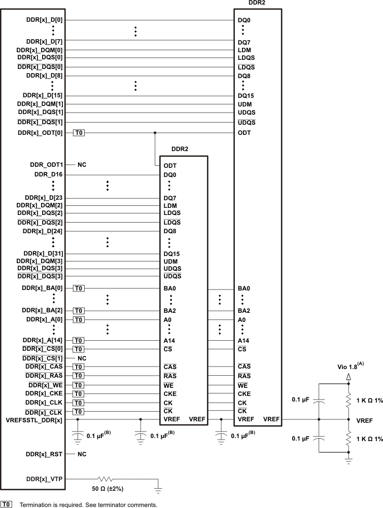
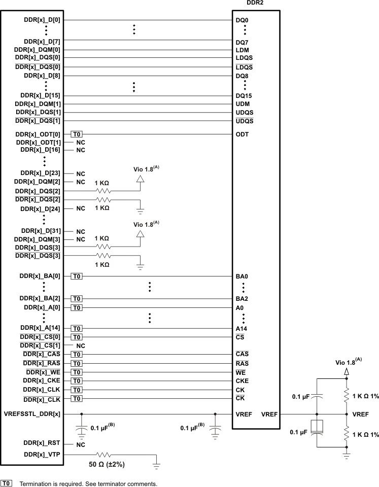
7.13.4.1.1.2 Compatible JEDEC DDR2 Devices
Table 7-54 shows the parameters of the JEDEC DDR2 devices that are compatible with this interface. Generally, the DDR2 interface is compatible with x16 DDR2-800 speed grade DDR2 devices.
Table 7-54 Compatible JEDEC DDR2 Devices (Per Interface)
| NO. | PARAMETER | MIN | MAX | UNIT |
|---|---|---|---|---|
| 1 | JEDEC DDR2 device speed grade(1) | DDR2-800 | ||
| 2 | JEDEC DDR2 device bit width | x16 | x16 | Bits |
| 3 | JEDEC DDR2 device count(2) | 1 | 2 | Devices |
| 4 | JEDEC DDR2 device ball count(3) | 84 | 92 | Balls |
7.13.4.1.1.3 PCB Stackup
The minimum stackup required for routing the AM387x device is a six-layer stackup as shown in Table 7-55. Additional layers may be added to the PCB stackup to accommodate other circuitry or to reduce the size of the PCB footprint.
Table 7-55 Minimum PCB Stackup
| LAYER | TYPE | DESCRIPTION |
|---|---|---|
| 1 | Signal | Top routing mostly horizontal |
| 2 | Plane | Ground |
| 3 | Plane | Power |
| 4 | Signal | Internal routing |
| 5 | Plane | Ground |
| 6 | Signal | Bottom routing mostly vertical |
Complete stackup specifications are provided in Table 7-56.
Table 7-56 PCB Stackup Specifications
| NO. | PARAMETER | MIN | TYP | MAX | UNIT |
|---|---|---|---|---|---|
| 1 | PCB routing/plane layers | 6 | |||
| 2 | Signal routing layers | 3 | |||
| 3 | Full ground layers under DDR2 routing region | 2 | |||
| 4 | Number of ground plane cuts allowed within DDR routing region | 0 | |||
| 5 | Number of ground reference planes required for each DDR2 routing layer | 1 | |||
| 6 | Number of layers between DDR2 routing layer and reference ground plane | 0 | |||
| 7 | PCB routing feature size | 4 | Mils | ||
| 8 | PCB trace width, w | 4 | Mils | ||
| 9 | PCB BGA escape via pad size(1) | 18 | 20 | Mils | |
| 10 | PCB BGA escape via hole size(1) | 10 | Mils | ||
| 11 | Processor BGA pad size | 0.4 | mm | ||
| 13 | Single-ended impedance, Zo | 50 | 75 | Ω | |
| 14 | Impedance control(2) | Z-5 | Z | Z+5 | Ω |
7.13.4.1.1.4 Placement
Figure 7-49 shows the required placement for the MPU as well as the DDR2 devices. The dimensions for this figure are defined in Table 7-57. The placement does not restrict the side of the PCB on which the devices are mounted. The ultimate purpose of the placement is to limit the maximum trace lengths and allow for proper routing space. For a 16-bit DDR memory system, the high-word DDR2 device is omitted from the placement.
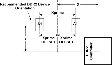 Figure 7-49 AM387x Device and DDR2 Device Placement
Table 7-57 Placement Specifications
| NO. | PARAMETER | MIN | MAX | UNIT |
|---|---|---|---|---|
| 1 | X + Y(1)(2) | 1660 | Mils | |
| 2 | X'(1)(2) | 1280 | Mils | |
| 3 | X' Offset(1)(2) (3) | 650 | Mils | |
| 4 | DDR2 keepout region(4) | |||
| 5 | Clearance from non-DDR2 signal to DDR2 keepout region(5) | 4 | w |
7.13.4.1.1.5 DDR2 Keepout Region
The region of the PCB used for the DDR2 circuitry must be isolated from other signals. The DDR2 keepout region is defined for this purpose and is shown in Figure 7-50. The size of this region varies with the placement and DDR routing. Additional clearances required for the keepout region are shown in Table 7-57.
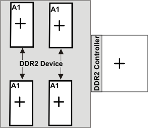 Figure 7-50 DDR2 Keepout Region
NOTE
The region shown in should encompass all the DDR2 circuitry and varies depending on placement. Non-DDR2 signals should not be routed on the DDR signal layers within the DDR2 keepout region. Non-DDR2 signals may be routed in the region, provided t hey are routed on layers separated from DDR2 signal layers by a ground layer. No breaks should be allowed in the reference ground layers in this region. In addition, the 1.8-V power plane should cover the entire keepout region. Routes for the two DDR interfaces must be separated by at least 4x; the more separation, the better.
7.13.4.1.1.6 Bulk Bypass Capacitors
Bulk bypass capacitors are required for moderate speed bypassing of the DDR2 and other circuitry. Table 7-58 contains the minimum numbers and capacitance required for the bulk bypass capacitors. Note that this table only covers the bypass needs of the DDR2 interfaces and DDR2 device. Additional bulk bypass capacitance may be needed for other circuitry.
Table 7-58 Bulk Bypass Capacitors
| No. | Parameter | Min | Max | Unit |
|---|---|---|---|---|
| 1 | DVDD18 bulk bypass capacitor count(1) | 6 | Devices | |
| 2 | DVDD18 bulk bypass total capacitance | 60 | μF | |
| 3 | DDR#1 bulk bypass capacitor count(1) | 1 | Devices | |
| 4 | DDR#1 bulk bypass total capacitance(1) | 10 | μF | |
| 5 | DDR#2 bulk bypass capacitor count(2) | 1 | Devices | |
| 6 | DDR#2 bulk bypass total capacitance(1)(2) | 10 | μF |
7.13.4.1.1.7 High-Speed Bypass Capacitors
High-speed (HS) bypass capacitors are critical for proper DDR2 interface operation. It is particularly important to minimize the parasitic series inductance of the HS bypass capacitors, MPU/DDR power, and MPU/DDR ground connections. Table 7-59 contains the specification for the HS bypass capacitors as well as for the power connections on the PCB.
Table 7-59 High-Speed Bypass Capacitors
| NO. | PARAMETER | MIN | MAX | UNIT |
|---|---|---|---|---|
| 1 | HS bypass capacitor package size(1) | 0402 | 10 Mils | |
| 2 | Distance from HS bypass capacitor to device being bypassed | 250 | Mils | |
| 3 | Number of connection vias for each HS bypass capacitor(2) | 2 | Vias | |
| 4 | Trace length from bypass capacitor contact to connection via | 1 | 30 | Mils |
| 5 | Number of connection vias for each MPU power/ground ball | 1 | Vias | |
| 6 | Trace length from MPU power/ground ball to connection via | 35 | Mils | |
| 7 | Number of connection vias for each DDR2 device power/ground ball | 1 | Vias | |
| 8 | Trace length from DDR2 device power/ground ball to connection via | 35 | Mils | |
| 9 | DVDD18 HS bypass capacitor count(3)(4) | 40 | Devices | |
| 10 | DVDD18 HS bypass capacitor total capacitance(4) | 2.4 | μF | |
| 11 | DDR device HS bypass capacitor count(3)(5) | 8 | Devices | |
| 12 | DDR device HS bypass capacitor total capacitance(5) | 0.4 | μF |
7.13.4.1.1.8 Net Classes
Table 7-60 lists the clock net classes for the DDR2 interface. Table 7-61 lists the signal net classes, and associated clock net classes, for the signals in the DDR2 interface. These net classes are used for the termination and routing rules that follow.
Table 7-60 Clock Net Class Definitions
| CLOCK NET CLASS | MPU PIN NAMES |
|---|---|
| CK | DDR[x]_CLK/DDR[x]_CLK |
| DQS0 | DDR[x]_DQS[0]/DDR[x]_DQS[0] |
| DQS1 | DDR[x]_DQS[1]/DDR[x]_DQS[1] |
| DQS2(1) | DDR[x]_DQS[2]/DDR[x]_DQS[2] |
| DQS3(1) | DDR[x]_DQS[3]/DDR[x]_DQS[3] |
Table 7-61 Signal Net Class Definitions
| CLOCK NET CLASS | ASSOCIATED CLOCK NET CLASS |
MPU PIN NAMES |
|---|---|---|
| ADDR_CTRL | CK | DDR[x]_BA[2:0], DDR[x]_A[14:0], DDR[x]_CS[x], DDR[x]_CAS, DDR[x]_RAS, DDR[x]_WE, DDR[x]_CKE, DDR[x]_ODT[x] |
| DQ0 | DQS0 | DDR[x]_D[7:0], DDR[x]_DQM[0] |
| DQ1 | DQS1 | DDR[x]_D[15:8], DDR[x]_DQM[1] |
| DQ2(1) | DQS2 | DDR[x]_D[23:16], DDR[x]_DQM[2] |
| DQ3(1) | DQS3 | DDR[x]_D[31:24], DDR[x]_DQM[3] |
7.13.4.1.1.9 DDR2 Signal Termination
Signal terminators are required in CK and ADDR_CTRL net classes. Serial terminators may be used on data lines to reduce EMI risk; however, serial terminations are the only type permitted. ODTs are integrated on the data byte net classes. They should be enabled to ensure signal integrity.Table 7-62 shows the specifications for the series terminators.
Table 7-62 DDR2 Signal Terminations
| NO. | PARAMETER | MIN | TYP | MAX | UNIT |
|---|---|---|---|---|---|
| 1 | CK net class(1)(2) | 0 | 10 | Ω | |
| 2 | ADDR_CTRL net class(1) (2)(3)(4) | 0 | 22 | Zo | Ω |
| 3 | Data byte net classes (DQS0-DQS3, DQ0-DQ3)(5) | 0 | Zo | Ω |
7.13.4.1.1.10 VREFSSTL_DDR Routing
VREFSSTL_DDR is used as a reference by the input buffers of the DDR2 memories as well as the MPU. VREF is intended to be half the DDR2 power supply voltage and should be created using a resistive divider as shown in Figure 7-48. Other methods of creating VREF are not recommended. Figure 7-51 shows the layout guidelines for VREF.
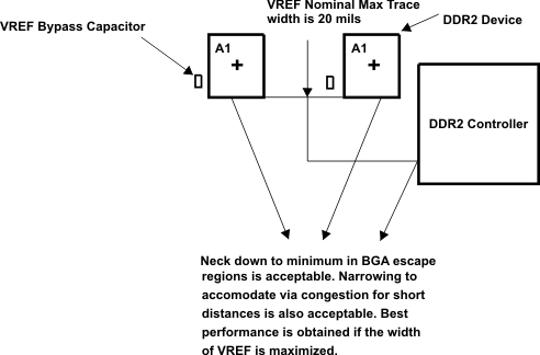 Figure 7-51 VREF Routing and Topology
7.13.4.1.2 DDR2 CK and ADDR_CTRL Routing
Figure 7-52 shows the topology of the routing for the CK and ADDR_CTRL net classes. The route is a balanced T as it is intended that the length of segments B and C be equal. In addition, the length of A (A'+A'') should be maximized.
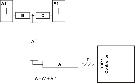 Figure 7-52 CK and ADDR_CTRL Routing and Topology
Table 7-63 CK and ADDR_CTRL Routing Specification (1)
| NO. | PARAMETER | MIN | TYP | MAX | UNIT |
|---|---|---|---|---|---|
| 1 | Center-to-center CK-CK spacing | 2w | |||
| 2 | CK/CK skew(1) | 25 | Mils | ||
| 3 | CK A-to-B/A-to-C skew length mismatch(2) | 25 | Mils | ||
| 4 | CK B-to-C skew length mismatch | 25 | Mils | ||
| 5 | Center-to-center CK to other DDR2 trace spacing(3) | 4w | |||
| 6 | CK/ADDR_CTRL nominal trace length(4) | CACLM-50 | CACLM | CACLM+50 | Mils |
| 7 | ADDR_CTRL-to-CK skew length mismatch | 100 | Mils | ||
| 8 | ADDR_CTRL-to-ADDR_CTRL skew length mismatch | 100 | Mils | ||
| 9 | Center-to-center ADDR_CTRL to other DDR2 trace spacing(3) | 4w | |||
| 10 | Center-to-center ADDR_CTRL to other ADDR_CTRL trace spacing(3) | 3w | |||
| 11 | ADDR_CTRL A-to-B/A-to-C skew length mismatch(2) | 100 | Mils | ||
| 12 | ADDR_CTRL B-to-C skew length mismatch | 100 | Mils |
Figure 7-53 shows the topology and routing for the DQS and DQ net classes; the routes are point to point. Skew matching across bytes is not needed nor recommended.
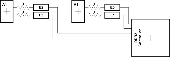 Figure 7-53 DQS and DQ Routing and Topology
Table 7-64 DQS and DQ Routing Specification
| NO. | PARAMETER | MIN | TYP | MAX | UNIT |
|---|---|---|---|---|---|
| 1 | Center-to-center DQS-DQSn spacing in E0|E1|E2|E3 | 2w | |||
| 2 | DQS-DQSn skew in E0|E1|E2|E3 | 25 | Mils | ||
| 3 | Center-to-center DQS to other DDR2 trace spacing(1) | 4w | |||
| 4 | DQS/DQ nominal trace length (2)(3)(4) | DQLM-50 | DQLM | DQLM+50 | Mils |
| 5 | DQ-to-DQS skew length mismatch(2)(3)(4) | 100 | Mils | ||
| 6 | DQ-to-DQ skew length mismatch(2)(3)(4) | 100 | Mils | ||
| 7 | DQ-to-DQ/DQS via count mismatch(2)(3)(4) | 1 | Vias | ||
| 8 | Center-to-center DQ to other DDR2 trace spacing(1)(5) | 4w | |||
| 9 | Center-to-center DQ to other DQ trace spacing(1)(6)(7) | 3w | |||
| 10 | DQ/DQS E skew length mismatch(2)(3)(4) | 100 | Mils |
7.13.4.2 DDR3 Routing Specifications
7.13.4.2.1 DDR3 versus DDR2
This specification only covers PCB designs that utilize DDR3 memory. PCB designs using other types of DDR memory should follow the specification appropriate for that type of memory. It is currently not possible to design a single PCB that supports multiple types of DDR memory.
7.13.4.2.2 DDR3 EMIFs
A processor may contain more than one EMIF. This specification covers only one EMIF and must be implemented for each additional EMIF. Requirements are identical between the EMIFs, however, the PCB layouts will most likely be different.
7.13.4.2.3 DDR3 Device Combinations
Because there are several possible combinations of device counts and single- or dual-side mounting, Table 7-65 summarizes the supported device configurations.
Table 7-65 Supported DDR3 Device Combinations(1)
| NUMBER OF DDR3 DEVICES | DDR3 DEVICE WIDTH (BITS) | MIRRORED? | DDR3 EMIF WIDTH (BITS) |
|---|---|---|---|
| 1 | 16 | N | 16 |
| 2 | 8 | Y(2) | 16 |
| 2 | 16 | N | 32 |
| 2 | 16 | Y(2) | 32 |
| 4 | 8 | N | 32 |
| 4 | 8 | Y(3) | 32 |
7.13.4.2.4 DDR3 Interface Schematic
The DDR3 interface schematic varies, depending upon the width of the DDR3 devices used and the width of the bus used (16 or 32 bits). General connectivity is straightforward and very similar. 16-bit DDR devices look like two 8-bit devices. Figure 7-54 and Figure 7-55 show the schematic connections for 32-bit interfaces using x16 and x8 devices.
Note that a 16-bit wide interface schematic is practically identical to the 32-bit interface; only the high-word DDR memories are removed.
When not using all or part of a DDR3 interface, the proper method of handling the unused pins is to tie off the DDR[x]_DQS[n] pins to the corresponding DVDD_DDR[x] supply via a 1-kΩ resistor and pulling the DDR[x]_DQS[n] pins to ground via a 1k-Ω resistor. This must be done for each byte not used. Although these signals have internal pullups and pulldowns, external pullups and pulldowns provide additional protection against external electrical noise causing activity on the signals.Also, include the 50-Ω pulldown for DDR[x]_VTP. The DVDD_DDR[x] and VREFSSTL_DDR[x] power supply pins must be connected to their respective power supplies even if DDR[x] is not being used. All other DDR interface pins can be left unconnected. Note that the supported modes for use of the DDR EMIF are 32 bits wide, 16 bits wide, or not used.
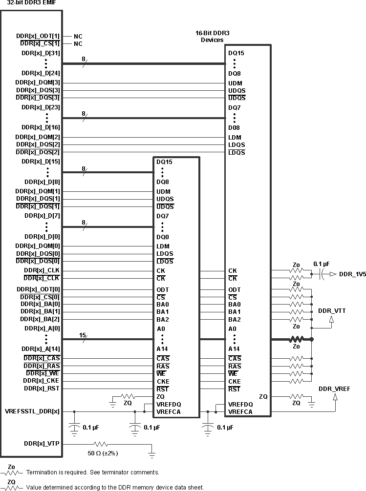 Figure 7-54 32-Bit, One-Bank DDR3 Interface Schematic Using Two 16-Bit DDR3 Devices
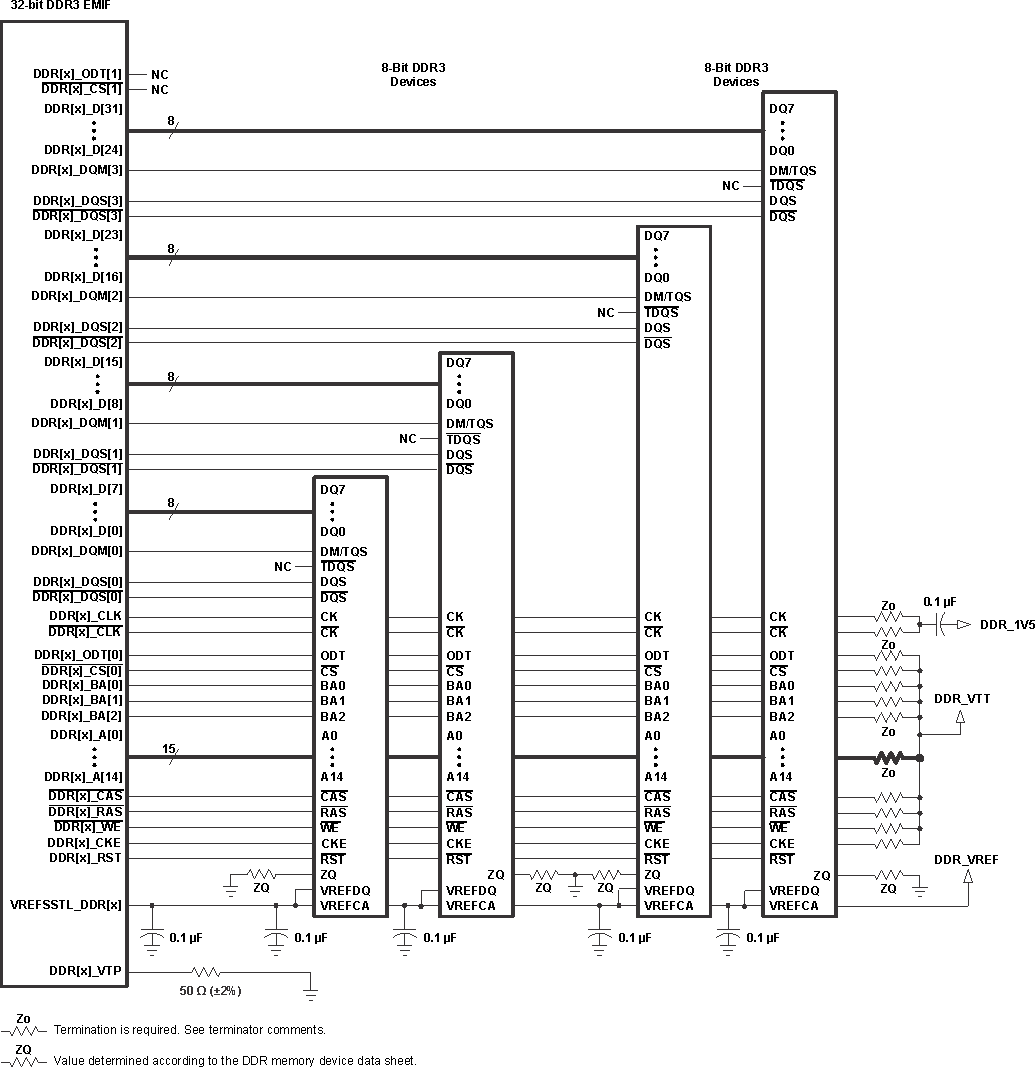 Figure 7-55 32-Bit, One-Bank DDR3 Interface Schematic Using Four 8-Bit DDR3 Devices
7.13.4.2.4.1 Compatible JEDEC DDR3 Devices
Table 7-66 shows the parameters of the JEDEC DDR3 devices that are compatible with this interface. Generally, the DDR3 interface is compatible with DDR3-1600 devices in the x8 or x16 widths.
Table 7-66 Compatible JEDEC DDR3 Devices (Per Interface)
| NO. | PARAMETER | MIN | MAX | UNIT |
|---|---|---|---|---|
| 1 | JEDEC DDR3 device speed grade(1) | DDR3-800 | DDR3-1600(3) | |
| 2 | JEDEC DDR3 device bit width | x8 | x16 | Bits |
| 3 | JEDEC DDR3 device count(2) | 2 | 8 | Devices |
7.13.4.2.4.2 PCB Stackup
The minimum stackup for routing the DDR3 interface is a four-layer stack up as shown in Table 7-67. Additional layers may be added to the PCB stackup to accommodate other circuitry, enhance SI/EMI performance, or to reduce the size of the PCB footprint. A six-layer stackup is shown in Table 7-68. Complete stackup specifications are provided in Table 7-69.
Table 7-67 Minimum PCB Stackup
| LAYER | TYPE | DESCRIPTION |
|---|---|---|
| 1 | Signal | Top routing mostly vertical |
| 2 | Plane | Split power plane |
| 3 | Plane | Full ground plane |
| 4 | Signal | Bottom routing mostly horizontal |
Table 7-68 Six-Layer PCB Stackup Suggestion
| LAYER | TYPE | DESCRIPTION |
|---|---|---|
| 1 | Signal | Top routing mostly vertical |
| 2 | Plane | Ground |
| 3 | Plane | Split power plane |
| 4 | Plane | Split power plane or Internal routing |
| 5 | Plane | Ground |
| 6 | Signal | Bottom routing mostly horizontal |
Table 7-69 PCB Stackup Specifications
| NO. | PARAMETER | MIN | TYP | MAX | UNIT |
|---|---|---|---|---|---|
| 1 | PCB routing/plane layers | 4 | 6 | ||
| 2 | Signal routing layers | 2 | |||
| 3 | Full ground reference layers under DDR3 routing region(1) | 1 | |||
| 4 | Full 1.5-V power reference layers under the DDR3 routing region(1) | 1 | |||
| 5 | Number of reference plane cuts allowed within DDR routing region(2) | 0 | |||
| 6 | Number of layers between DDR3 routing layer and reference plane(3) | 0 | |||
| 7 | PCB routing feature size | 4 | Mils | ||
| 8 | PCB trace width, w | 4 | Mils | ||
| 13 | Single-ended impedance, Zo | 50 | 75 | Ω | |
| 14 | Impedance control(4) | Z-5 | Z | Z+5 | Ω |
7.13.4.2.4.3 Placement
Figure 7-56 shows the required placement for the processor as well as the DDR3 devices. The dimensions for this figure are defined in Table 7-70. The placement does not restrict the side of the PCB on which the devices are mounted. The ultimate purpose of the placement is to limit the maximum trace lengths and allow for proper routing space. For a 16-bit DDR memory system, the high-word DDR3 device(s) are omitted from the placement.
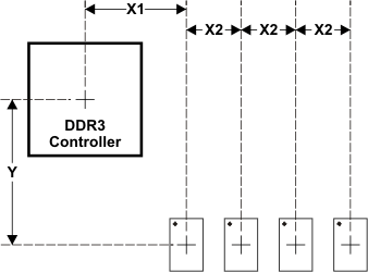 Figure 7-56 Placement Specifications
It is strongly recommended that high-speed bypass capacitors be placed and accommodated for during the placement and route planning phase. It is very difficult to add bypass capacitors once the board has been routed and significant rework may be required to meet the high-speed bypass capacitor requirements in Section 7.13.4.2.4.6, High-Speed Bypass Capacitors if the proper planning is not done. A particular challenge to placing bypass capacitors in congested areas is fitting the required vias. It is suggested that each pair of vias support two bypass capacitors by mounting one capacitor on the top of the board and other on the bottom. Do not share vias between capacitors mounted on the same side of the PCB. Another suggestion is to line up the vias for the bypass capacitors for the processor in rows forming channels to allow the signals to escape.
Table 7-70 Placement Specifications
| NO. | PARAMETER | MIN | MAX | UNIT |
|---|---|---|---|---|
| 1 | X1(1)(2)(3) | 1000 | Mils | |
| 2 | X2(1)(2) | 600 | Mils | |
| 3 | Y Offset(1)(2)(3) | 1500 | Mils | |
| 4 | DDR3 keepout region | |||
| 5 | Clearance from non-DDR3 signal to DDR3 keepout region(4)(5)(6) | 4 | w |
7.13.4.2.4.4 DDR3 Keepout Region
The region of the PCB used for DDR3 circuitry must be isolated from other signals. The DDR3 keepout region is defined for this purpose and is shown in Figure 7-57. The size of this region varies with the placement and DDR routing. Additional clearances required for the keepout region are shown in Table 7-70. Non-DDR3 signals should not be routed on the DDR signal layers within the DDR3 keepout region. Non-DDR3 signals may be routed in the region, provided they are routed on layers separated from the DDR signal layers by a ground layer. No breaks should be allowed in the reference ground layers in this region. In addition, the 1.5-V DDR3 power plane should cover the entire keepout region. Also note that if there is more than one DDR controller, the signals from each controller must be separated from each other by the specification in Table 7-70, item 5. Each DDR controller should have its own DDR keepout region.
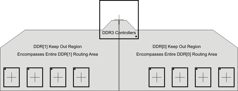 Figure 7-57 DDR3 Keepout Region
Figure 7-57 is an example of a processor with two DDR controllers. Processors with a single DDR controler will have only one DDR keepout region. Each DDR controller should have its own keepout region.
7.13.4.2.4.5 Bulk Bypass Capacitors
Bulk bypass capacitors are required for moderate speed bypassing of the DDR3 and other circuitry. Table 7-71 contains the minimum numbers and capacitance required for the bulk bypass capacitors. Note that this table only covers the bypass needs of the DDR3 controllers and DDR3 device(s). Additional bulk bypass capacitance may be needed for other circuitry.
Table 7-71 Bulk Bypass Capacitors Per DDR3 EMIF
| NO. | PARAMETER | MIN | MAX | UNIT |
|---|---|---|---|---|
| 1 | DDR_1V5 bulk bypass capacitor count(1) | 3 | Devices | |
| 2 | DDR_1V5 bulk bypass total capacitance | 70 | μF |
7.13.4.2.4.6 High-Speed Bypass Capacitors
High-speed (HS) bypass capacitors are critical for proper DDR3 interface operation. It is particularly important to minimize the parasitic series inductance of the HS bypass capacitors, processor/DDR power, and processor/DDR ground connections. Table 7-72 contains the specification for the HS bypass capacitors as well as for the power connections on the PCB. Generally speaking, it is good to:
- Fit as many HS bypass capacitors as possible.
- Minimize the distance from the bypass capacitor to the pins/balls being bypassed.
- Use the smallest physical sized capacitor possible with the highest capacitance readily available.
- Connect the bypass capacitor pads to their vias using the widest traces possible and using the largest hole size via possible.
- Minimize via sharing. Note the limits on via sharing shown in Table 7-72.
Table 7-72 High-Speed Bypass Capacitors
| NO. | PARAMETER | MIN | TYP | MAX | UNIT |
|---|---|---|---|---|---|
| 1 | HS bypass capacitor package size(1) | 201 | 402 | 10 Mils | |
| 2 | Distance, HS bypass capacitor to processor being bypassed(2)(3)(4) | 400 | Mils | ||
| 3 | Processor DDR_1V5 HS bypass capacitor count(11) | 35 | Per DDR3 EMIF |
||
| 4 | Processor DDR_1V5 HS bypass capacitor total capacitance | 5 | μF | ||
| 5 | Number of connection vias for each device power/ground ball(5) | Vias | |||
| 6 | Trace length from device power/ground ball to connection via(2) | 35 | 70 | Mils | |
| 7 | Distance, HS bypass capacitor to DDR device being bypassed(6) | 150 | Mils | ||
| 8 | DDR3 device HS bypass capacitor count(7) | 12 | Devices | ||
| 9 | DDR3 device HS bypass capacitor total capacitance(7) | 0.85 | μF | ||
| 10 | Number of connection vias for each HS capacitor(8)(9) | 2 | Vias | ||
| 11 | Trace length from bypass capacitor connect to connection via(2)(9) | 35 | 100 | Mils | |
| 12 | Number of connection vias for each DDR3 device power/ground ball(10) | 1 | Vias | ||
| 13 | Trace length from DDR3 device power/ground ball to connection via(2)(8) | 35 | 60 | Mils |
7.13.4.2.4.6.1 Return Current Bypass Capacitors and Vias
If a power plane is used as a reference plane then additional bypass capacitors may be required to accommodate the signal return currents. Care should be taken to minimize the layer transitions during routing. If a layer transition is necessary, it is better to transition to a layer using the same reference plane. If this cannot be accommodated, ensure there is a nearby path to allow the return currents to transition between reference planes. Transitions from power reference planes to ground reference planes must go through a bypass capacitor. Transition between different ground references or DVDD_DDR planes can go through a connecting via. As many of these return current bypass capacitors or vias should be used as possible. The goal is to minimize the size of the return current loops. Generally, this type of situation happens where signals must transition from horizontal to vertical routing and vice-versa.
7.13.4.2.4.7 Net Classes
Table 7-73 lists the clock net classes for the DDR3 interface. Table 7-74 lists the signal net classes, and associated clock net classes, for signals in the DDR3 interface. These net classes are used for the termination and routing rules that follow.
Table 7-73 Clock Net Class Definitions
| CLOCK NET CLASS | PROCESSOR PIN NAMES |
|---|---|
| CK | DDR[x]_CLK/DDR[x]_CLK |
| DQS0 | DDR[x]_DQS[0]/DDR[x]_DQS[0] |
| DQS1 | DDR[x]_DQS[1]/DDR[x]_DQS[1] |
| DQS2(1) | DDR[x]_DQS[2]/DDR[x]_DQS[2] |
| DQS3(1) | DDR[x]_DQS[3]/DDR[x]_DQS[3] |
Table 7-74 Signal Net Class Definitions
| CLOCK NET CLASS | ASSOCIATED CLOCK NET CLASS |
PROCESSOR PIN NAMES |
|---|---|---|
| ADDR_CTRL | CK | DDR[x]_BA[2:0], DDR[x]_A[14:0], DDR[x]_CS[x], DDR[x]_CAS, DDR[x]_RAS, DDR[x]_WE, DDR[x]_CKE, DDR[x]_ODT[x] |
| DQ0 | DQS0 | DDR[x]_D[7:0], DDR[x]_DQM[0] |
| DQ1 | DQS1 | DDR[x]_D[15:8], DDR[x]_DQM[1] |
| DQ2(1) | DQS2 | DDR[x]_D[23:16], DDR[x]_DQM[2] |
| DQ3(1) | DQS3 | DDR[x]_D[31:24], DDR[x]_DQM[3] |
7.13.4.2.4.8 DDR3 Signal Termination
Signal terminators are required for the CK and ADDR_CTRL net classes. The data lines are terminated by ODT and, thus, the PCB traces should be unterminated. Detailed termination specifications are covered in the routing rules in the following sections.
7.13.4.2.4.9 VREFSSTL_DDR Routing
VREFSSTL_DDR (VREF) is used as a reference by the input buffers of the DDR3 memories as well as the processor. VREF is intended to be half the DDR3 power supply voltage and is typically generated with the DDR3 1.5-V and VTT power supply. It should be routed as a nominal 20-mil wide trace with 0.1 µF bypass capacitors near each device connection. Narrowing of VREF is allowed to accommodate routing congestion.
7.13.4.2.4.10 VTT
Like VREF, the nominal value of the VTT supply is half the DDR3 supply voltage. Unlike VREF, VTT is expected to source and sink current, specifically the termination current for the ADDR_CTRL net class Thevinen terminators. VTT is needed at the end of the address bus and it should be routed as a power sub-plane. VTT should be bypassed near the terminator resistors.
7.13.4.2.4.11 CK and ADDR_CTRL Topologies and Routing Definition
The CK and ADDR_CTRL net classes are routed similarly and are length matched to minimize skew between them. CK is a bit more complicated because it runs at a higher transition rate and is differential. The following subsections show the topology and routing for various DDR3 configurations for CK and ADDR_CTRL. Only the components shown in the topologies are allowed. Items such as test points and additional terminations are specifically disallowed. The figures in the following subsections define the terms for the routing specification detailed in Table 7-75.
Care should be taken to minimize layer transitions during routing. If a layer transition is necessary, it is better to transition to a layer using the same reference plane. If this cannot be accommodated, ensure there are nearby ground vias to allow the return currents to transition between reference planes if both reference planes are ground or DVDD_DDR. Ensure there are nearby bypass capacitors to allow the return currents to transition between reference planes if one of the reference planes is ground. The goal is to minimize the size of the return current loops.
7.13.4.2.4.11.1 Four DDR3 Devices
Four DDR3 devices are supported on the DDR EMIF consisting of four x8 DDR3 devices arranged as one bank (CS). These four devices may be mounted on a single side of the PCB, or may be mirrored in two pairs to save board space at a cost of increased routing complexity and parts on the backside of the PCB.
7.13.4.2.4.11.1.1 CK and ADDR_CTRL Topologies, Four DDR3 Devices
Figure 7-58 shows the topology of the CK net classes and Figure 7-59 shows the topology for the corresponding ADDR_CTRL net classes.
7.13.4.2.4.11.1.2 CK and ADDR_CTRL Routing, Four DDR3 Devices
Figure 7-60 shows the CK routing for four DDR3 devices placed on the same side of the PCB. Figure 7-61 shows the corresponding ADDR_CTRL routing.
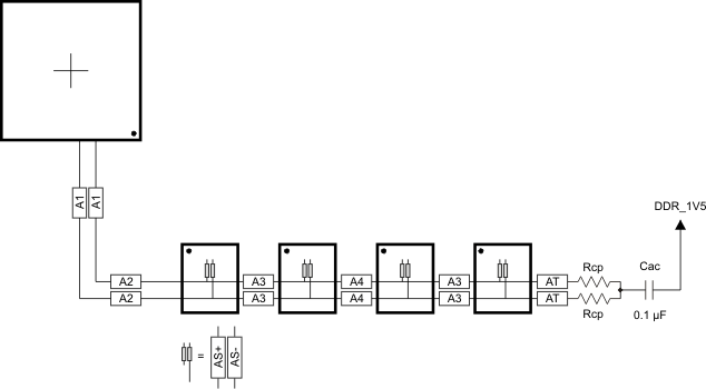 Figure 7-60 CK Routing for Four Single-Side DDR3 Devices
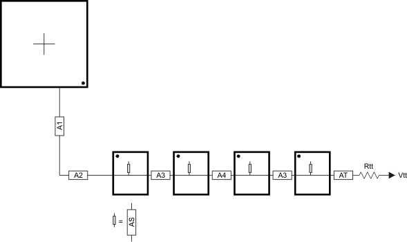 Figure 7-61 ADDR_CTRL Routing for Four Single-Side DDR3 Devices
To save PCB space, the four DDR3 memories may be mounted as two mirrored pairs at a cost of increased routing and assembly complexity. Figure 7-62 and Figure 7-63 show the routing for CK and ADDR_CTRL, respectively, for four DDR3 devices mirrored in a two-pair configuration.
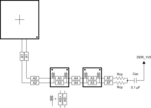 Figure 7-62 CK Routing for Four Mirrored DDR3 Devices
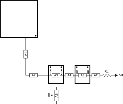 Figure 7-63 ADDR_CTRL Routing for Four Mirrored DDR3 Devices
7.13.4.2.4.11.2 Two DDR3 Devices
Two DDR3 devices are supported on the DDR EMIF consisting of two x8 DDR3 devices arranged as one bank (CS), 16-bits wide, or two x16 DDR3 devices arranged as one bank (CS), 32-bits wide. These two devices may be mounted on a single side of the PCB, or may be mirrored in a pair to save board space at a cost of increased routing complexity and parts on the backside of the PCB.
7.13.4.2.4.11.2.1 CK and ADDR_CTRL Topologies, Two DDR3 Devices
Figure 7-64 shows the topology of the CK net classes and Figure 7-65 shows the topology for the corresponding ADDR_CTRL net classes.
7.13.4.2.4.11.2.2 CK and ADDR_CTRL Routing, Two DDR3 Devices
Figure 7-66 shows the CK routing for two DDR3 devices placed on the same side of the PCB. Figure 7-67 shows the corresponding ADDR_CTRL routing.
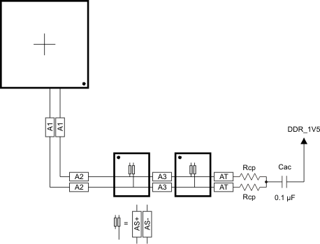 Figure 7-66 CK Routing for Two Single-Side DDR3 Devices
 Figure 7-67 ADDR_CTRL Routing for Two Single-Side DDR3 Devices
To save PCB space, the two DDR3 memories may be mounted as a mirrored pair at a cost of increased routing and assembly complexity. Figure 7-68 and Figure 7-69 show the routing for CK and ADDR_CTRL, respectively, for two DDR3 devices mirrored in a single-pair configuration.
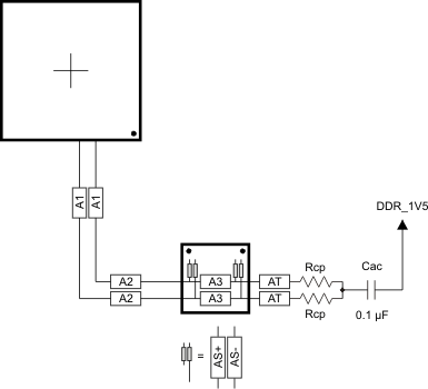 Figure 7-68 CK Routing for Two Mirrored DDR3 Devices
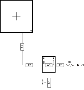 Figure 7-69 ADDR_CTRL Routing for Two Mirrored DDR3 Devices
7.13.4.2.4.11.3 One DDR3 Device
A single DDR3 device is supported on the DDR EMIF consisting of one x16 DDR3 device arranged as one bank (CS), 16-bits wide.
7.13.4.2.4.11.3.1 CK and ADDR_CTRL Topologies, One DDR3 Device
Figure 7-70 shows the topology of the CK net classes and Figure 7-71 shows the topology for the corresponding ADDR_CTRL net classes.
7.13.4.2.4.11.3.2 CK and ADDR/CTRL Routing, One DDR3 Device
Figure 7-72 shows the CK routing for one DDR3 device placed on the same side of the PCB. Figure 7-73 shows the corresponding ADDR_CTRL routing.
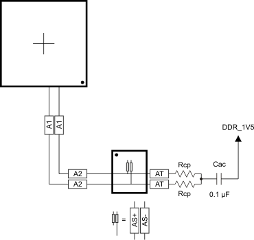 Figure 7-72 CK Routing for One DDR3 Device
 Figure 7-73 ADDR_CTRL Routing for One DDR3 Device
7.13.4.2.4.12 Data Topologies and Routing Definition
No matter the number of DDR3 devices used, the data line topology is always point-to-point, so its definition is simple.
Care should be taken to minimize layer transitions during routing. If a layer transition is necessary, it is better to transition to a layer using the same reference plane. If this cannot be accommodated, ensure there are nearby ground vias to allow the return currents to transition between reference planes if both reference planes are ground or DVDD_DDR. Ensure there are nearby bypass capacitors to allow the return currents to transition between reference planes if one of the reference planes is ground. The goal is to minimize the size of the return current loops.
7.13.4.2.4.12.1 DQS and DQ/DM Topologies, Any Number of Allowed DDR3 Devices
DQS lines are point-to-point differential, and DQ/DM lines are point-to-point singled ended. Figure 7-74 and Figure 7-75 show these topologies.
7.13.4.2.4.12.2 DQS and DQ/DM Routing, Any Number of Allowed DDR3 Devices
Figure 7-76 and Figure 7-77 show the DQS and DQ/DM routing.
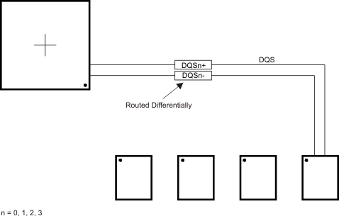 Figure 7-76 DQS Routing With Any Number of Allowed DDR3 Devices
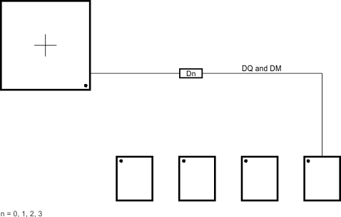 Figure 7-77 DQ/DM Routing With Any Number of Allowed DDR3 Devices
7.13.4.2.4.13 Routing Specification
7.13.4.2.4.13.1 CK and ADDR_CTRL Routing Specification
Skew within the CK and ADDR_CTRL net classes directly reduces setup and hold margin and, thus, this skew must be controlled. The only way to practically match lengths on a PCB is to lengthen the shorter traces up to the length of the longest net in the net class and its associated clock. A metric to establish this maximum length is Manhattan distance. The Manhattan distance between two points on a PCB is the length between the points when connecting them only with horizontal or vertical segments. A reasonable trace route length is to within a percentage of its Manhattan distance. CACLM is defined as Clock Address Control Longest Manhattan distance.
Given the clock and address pin locations on the processor and the DDR3 memories, the maximum possible Manhattan distance can be determined given the placement. Figure 7-78 and Figure 7-79 show this distance for four loads and two loads, respectively. It is from this distance that the specifications on the lengths of the transmission lines for the address bus are determined. CACLM is determined similarly for other address bus configurations; i.e., it is based on the longest net of the CK/ADDR_CTRL net class. For CK and ADDR_CTRL routing, these specifications are contained in Table 7-75.
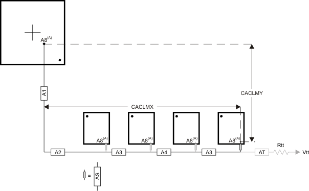
The length of shorter CK/ADDR_CTRL stubs as well as the length of the terminator stub are not included in this length calculation. Nonincluded lengths are grayed out in the figure.
Assuming A8 is the longest, CALM = CACLMY + CACLMX + 300 mils.
The extra 300 mils allows for routing down lower than the DDR3 memories and returning up to reach A8.
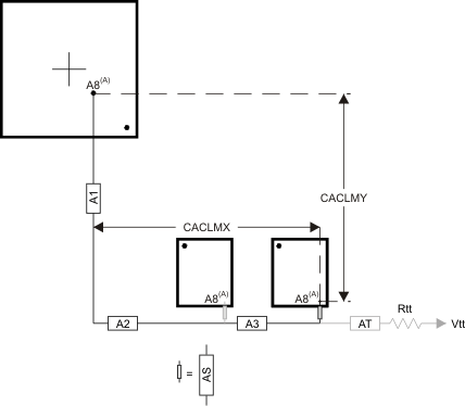
Table 7-75 CK and ADDR_CTRL Routing Specification(1)(2)
| NO. | PARAMETER | MIN | TYP | MAX | UNIT |
|---|---|---|---|---|---|
| 1 | A1+A2 length | 2500 | mils | ||
| 2 | A1+A2 skew | 25 | mils | ||
| 3 | A3 length | 660 | mils | ||
| 4 | A3 skew(3) | 25 | mils | ||
| 5 | A3 skew(4) | 125 | mils | ||
| 6 | A4 length | 660 | mils | ||
| 7 | A4 skew | 25 | mils | ||
| 8 | AS length | 100 | mils | ||
| 9 | AS skew | 100 | mils | ||
| 10 | AS+/AS- length | 70 | mils | ||
| 11 | AS+/AS- skew | 5 | mils | ||
| 12 | AT length(5) | 500 | mils | ||
| 13 | AT skew(6) | 100 | mils | ||
| 14 | AT skew(7) | 5 | mils | ||
| 15 | CK/ADDR_CTRL nominal trace length(8) | CACLM-50 | CACLM | CACLM+50 | mils |
| 16 | Center-to-center CK to other DDR3 trace spacing(9) | 4w | |||
| 17 | Center-to-center ADDR_CTRL to other DDR3 trace spacing(9)(10) | 4w | |||
| 18 | Center-to-center ADDR_CTRL to other ADDR_CTRL trace spacing(9) | 3w | |||
| 19 | CK center-to-center spacing(11) | (12) | |||
| 20 | CK spacing to other net(9) | 4w | |||
| 21 | Rcp(13) | Zo-1 | Zo | Zo+ | Ω |
| 22 | Rtt(13)(14) | Zo-5 | Zo | Zo+5 | Ω |
7.13.4.2.4.13.2 DQS and DQ Routing Specification
Skew within the DQS and DQ/DM net classes directly reduces setup and hold margin and thus this skew must be controlled. The only way to practically match lengths on a PCB is to lengthen the shorter traces up to the length of the longest net in the net class and its associated clock. As with CK and ADDR_CTRL, a reasonable trace route length is to within a percentage of its Manhattan distance. DQLMn is defined as DQ Longest Manhattan distance n, where n is the byte number. For a 32-bit interface, there are four DQLMs, DQLM0–DQLM3. Likewise, for a 16-bit interface, there are two DQLMs, DQLM0–DQLM1.
NOTE
It is not required, nor is it recommended, to match the lengths across all bytes. Length matching is only required within each byte.
Given the DQS and DQ/DM pin locations on the MPU and the DDR3 memories, the maximum possible Manhattan distance can be determined given the placement. Figure 7-80 shows this distance for four loads. It is from this distance that the specifications on the lengths of the transmission lines for the data bus are determined. For DQS and DQ/DM routing, these specifications are contained in Table 7-76.
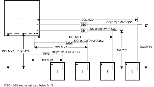
DQLM0 = DQLMX0 + DQLMY0
DQLM1 = DQLMX1 + DQLMY1
DQLM2 = DQLMX2 + DQLMY2
DQLM3 = DQLMX3 + DQLMY3
Table 7-76 Data Routing Specification(1)
| NO. | PARAMETER | MIN | TYP | MAX | UNIT |
|---|---|---|---|---|---|
| 1 | DB0 nominal length(2)(3) | DQLM0 | mils | ||
| 2 | DB1 nominal length(2)(4) | DQLM1 | mils | ||
| 3 | DB2 nominal length(2)(5) | DQLM2 | mils | ||
| 4 | DB3 nominal length(2)(6) | DQLM3 | mils | ||
| 5 | DBn skew(7) | 25 | mils | ||
| 6 | DQSn+ to DQSn- skew | 5 | mils | ||
| 7 | DQSn to DBn skew(7)(8) | 25 | mils | ||
| 8 | Center-to-center DBn to other DDR3 trace spacing(9)(10) | 4w | |||
| 9 | Center-to-center DBn to other DBn trace spacing(9)(11) | 3w | |||
| 10 | DQSn center-to-center spacing(12) | (13) | |||
| 11 | DQSn center-to-center spacing to other net(9) | 4w |
7.14 Multichannel Audio Serial Port (McASP)
The multichannel audio serial port (McASP) functions as a general-purpose audio serial port optimized for the needs of multichannel audio applications. The McASP is useful for time-division multiplexed (TDM) stream, Inter-Integrated Sound (I2S) protocols, and inter-component digital audio interface transmission (DIT).
7.14.1 McASP Device-Specific Information
The device includes six multichannel audio serial port (McASP) interface peripherals (McASP0, McASP1, McASP2, McASP3, McASP4, and McASP5). The McASP module consists of a transmit and receive section. On McASP0/1, these sections can operate completely independently with different data formats, separate master clocks, bit clocks, and frame syncs or, alternatively, the transmit and receive sections may be synchronized. On McASP2, McASP3, McASP4, and McASP5, the transmit and receive sections must always be synchronized. The McASP module also includes shift registers that may be configured to operate as either transmit data or receive data.
The transmit section of the McASP can transmit data in either a time-division-multiplexed (TDM) synchronous serial format or in a digital audio interface (DIT) format where the bit stream is encoded for S/PDIF, AES-3, IEC-60958, CP-430 transmission. The receive section of the McASP peripheral supports the TDM synchronous serial format.
The McASP module can support one transmit data format (either a TDM format or DIT format) and one receive format at a time. All transmit shift registers use the same format and all receive shift registers use the same format; however, the transmit and receive formats need not be the same. Both the transmit and receive sections of the McASP also support burst mode, which is useful for nonaudio data (for example, passing control information between two devices).
The McASP peripheral has additional capability for flexible clock generation and error detection/handling, as well as error management.
The device McASP0 and McASP1 modules have up to 10 serial data pins, while McASP2, McASP3, McASP4, and McASP5 are limited to up to four serial data pins each. The McASP FIFO size is 256 bytes and two DMA and two interrupt requests are supported. Buffers are used transparently to better manage DMA, which can be leveraged to manage data flow more efficiently.
For more detailed information on and the functionality of the McASP peripheral, see the Multichannel Audio Serial Port (McASP) chapter of the AM387x Sitara™ ARM Processors Technical Reference Manual (Literature Number: SPRUGZ7).
7.14.2 McASP0, McASP1, McASP2, McASP3, McASP4, and McASP5 Peripheral Registers Descriptions
Table 7-77 McASP0/1/2/3/4/5 Registers
| HEX ADDRESS RANGE | ACRONYM | REGISTER NAME | |||||
|---|---|---|---|---|---|---|---|
| MCASP0 | MCASP1 | MCASP2 | MCASP3 | MCASP4 | MCASP5 | ||
| 0x4803 8000 | 0x4803 C000 | 0x4805 0000 | 0x4A1A 2000 | 0x4A1A 8000 | 0x4A1A E000 | PID | Peripheral ID |
| 0x4803 8010 | 0x4803 C010 | 0x4805 0010 | 0x4A1A 2010 | 0x4A1A 8010 | 0x4A1A E010 | PFUNC | Pin Function |
| 0x4803 8014 | 0x4803 C014 | 0x4805 0014 | 0x4A1A 2014 | 0x4A1A 8014 | 0x4A1A E014 | PDIR | Pin Direction |
| 0x4803 8018 | 0x4803 C018 | 0x4805 0018 | 0x4A1A 2018 | 0x4A1A 8018 | 0x4A1A E018 | PDOUT | Pin Data Out |
| 0x4803 801C | 0x4803 C01C | 0x4805 001C | 0x4A1A 201C | 0x4A1A 801C | 0x4A1A E01C | PDIN | Pin Data Input (Read) Read returns pin data input |
| PDSET | Pin Data Set (Write) Writes effect pin data set (Alternate Write Address PDOUT) |
||||||
| 0x4803 8020 | 0x4803 C020 | 0x4805 0020 | 0x4A1A 2020 | 0x4A1A 8020 | 0x4A1A E020 | PDCLR | Pin Data Clear (Alternate Write Address PDOUT) |
| 0x4803 8044 | 0x4803 C044 | 0x4805 0044 | 0x4A1A 2044 | 0x4A1A 8044 | 0x4A1A E044 | GBLCTL | Global Control |
| 0x4803 8048 | 0x4803 C048 | 0x4805 0048 | 0x4A1A 2048 | 0x4A1A 8048 | 0x4A1A E048 | AMUTE | Mute Control |
| 0x4803 804C | 0x4803 C04C | 0x4805 004C | 0x4A1A 204C | 0x4A1A 804C | 0x4A1A E04C | LBCTL | Loop-Back Test Control |
| 0x4803 8050 | 0x4803 C050 | 0x4805 0050 | 0x4A1A 2050 | 0x4A1A 8050 | 0x4A1A E050 | TXDITCTL | Transmit DIT Mode Control |
| 0x4803 8060 | 0x4803 C060 | 0x4805 0060 | 0x4A1A 2060 | 0x4A1A 8060 | 0x4A1A E060 | GBLCTLR | Alias of GBLCTL containing only receiver reset bits; allows transmit to be reset independently from receive |
| 0x4803 8064 | 0x4803 C064 | 0x4805 0064 | 0x4A1A 2064 | 0x4A1A 8064 | 0x4A1A E064 | RXMASK | Receiver Bit Mask |
| 0x4803 8068 | 0x4803 C068 | 0x4805 0068 | 0x4A1A 2068 | 0x4A1A 8068 | 0x4A1A E068 | RXFMT | Receive Bitstream Format |
| 0x4803 806C | 0x4803 C06C | 0x4805 006C | 0x4A1A 206C | 0x4A1A 806C | 0x4A1A E06C | RXFMCTL | Receive Frame Sync Control |
| 0x4803 8070 | 0x4803 C070 | 0x4805 0070 | 0x4A1A 2070 | 0x4A1A 8070 | 0x4A1A E070 | ACLKRCTL | Receive Clock Control |
| 0x4803 8074 | 0x4803 C074 | 0x4805 0074 | 0x4A1A 2074 | 0x4A1A 8074 | 0x4A1A E074 | AHCLKRCTL | High Frequency Receive Clock Control |
| 0x4803 8078 | 0x4803 C078 | 0x4805 0078 | 0x4A1A 2078 | 0x4A1A 8078 | 0x4A1A E078 | RXTDM | Receive TDM Slot 0-31 |
| 0x4803 807C | 0x4803 C07C | 0x4805 007C | 0x4A1A 207C | 0x4A1A 807C | 0x4A1A E07C | EVTCTLR | Receiver Interrupt Control |
| 0x4803 8080 | 0x4803 C080 | 0x4805 0080 | 0x4A1A 2080 | 0x4A1A 8080 | 0x4A1A E080 | RXSTAT | Status Receiver |
| 0x4803 8084 | 0x4803 C084 | 0x4805 0084 | 0x4A1A 2084 | 0x4A1A 8084 | 0x4A1A E084 | RXTDMSLOT | Current Receive TDM Slot |
| 0x4803 8088 | 0x4803 C088 | 0x4805 0088 | 0x4A1A 2088 | 0x4A1A 8088 | 0x4A1A E088 | RXCLKCHK | Receiver Clock Check Control |
| 0x4803 808C | 0x4803 C08C | 0x4805 008C | 0x4A1A 208C | 0x4A1A 808C | 0x4A1A E08C | REVTCTL | Receiver DMA Event Control |
| 0x4803 80A0 | 0x4803 C0A0 | 0x4805 00A0 | 0x4A1A 20A0 | 0x4A1A 80A0 | 0x4A1A E0A0 | GBLCTLX | Alias of GBLCTL containing only transmit reset bits; allows transmit to be reset independently from receive |
| 0x4803 80A4 | 0x4803 C0A4 | 0x4805 00A4 | 0x4A1A 20A4 | 0x4A1A 80A4 | 0x4A1A E0A4 | TXMASK | Transmit Format Unit Bit Mask |
| 0x4803 80A8 | 0x4803 C0A8 | 0x4805 00A8 | 0x4A1A 20A8 | 0x4A1A 80A8 | 0x4A1A E0A8 | TXFMT | Transmit Bitstream Format |
| 0x4803 80AC | 0x4803 C0AC | 0x4805 00AC | 0x4A1A 20AC | 0x4A1A 80AC | 0x4A1A E0AC | TXFMCTL | Transmit Frame Sync Control |
| 0x4803 80B0 | 0x4803 C0B0 | 0x4805 00B0 | 0x4A1A 20B0 | 0x4A1A 80B0 | 0x4A1A E0B0 | ACLKXCTL | Transmit Clock Control |
| 0x4803 80B4 | 0x4803 C0B4 | 0x4805 00B4 | 0x4A1A 20B4 | 0x4A1A 80B4 | 0x4A1A E0B4 | AHCLKXCTL | High Frequency Transmit Clock Control |
| 0x4803 80B8 | 0x4803 C0B8 | 0x4805 00B8 | 0x4A1A 20B8 | 0x4A1A 80B8 | 0x4A1A E0B8 | TXTDM | Transmit TDM Slot 0-31 |
| 0x4803 80BC | 0x4803 C0BC | 0x4805 00BC | 0x4A1A 20BC | 0x4A1A 80BC | 0x4A1A E0BC | EVTCTLX | Transmitter Interrupt Control |
| 0x4803 80C0 | 0x4803 C0C0 | 0x4805 00C0 | 0x4A1A 20C0 | 0x4A1A 80C0 | 0x4A1A E0C0 | TXSTAT | Status Transmitter |
| 0x4803 80C4 | 0x4803 C0C4 | 0x4805 00C4 | 0x4A1A 20C4 | 0x4A1A 80C4 | 0x4A1A E0C4 | TXTDMSLOT | Current Transmit TDM Slot |
| 0x4803 80C8 | 0x4803 C0C8 | 0x4805 00C8 | 0x4A1A 20C8 | 0x4A1A 80C8 | 0x4A1A E0C8 | TXCLKCHK | Transmit Clock Check Control |
| 0x4803 80CC | 0x4803 C0CC | 0x4805 00CC | 0x4A1A 20CC | 0x4A1A 80CC | 0x4A1A E0CC | XEVTCTL | Transmitter DMA Control |
| 0x4803 80D0 | 0x4803 C0D0 | 0x4805 00D0 | 0x4A1A 20D0 | 0x4A1A 80D0 | 0x4A1A E0D0 | CLKADJEN | One-shot Clock Adjust Enable |
| 0x4803 8100 | 0x4803 C100 | 0x4805 0100 | 0x4A1A 2100 | 0x4A1A 8100 | 0x4A1A E100 | DITCSRA0 | Left (Even TDM Slot) Channel Status Register File |
| 0x4803 8104 | 0x4803 C104 | 0x4805 0104 | 0x4A1A 2104 | 0x4A1A 8104 | 0x4A1A E104 | DITCSRA1 | Left (Even TDM Slot) Channel Status Register File |
| 0x4803 8108 | 0x4803 C108 | 0x4805 0108 | 0x4A1A 2108 | 0x4A1A 8108 | 0x4A1A E108 | DITCSRA2 | Left (Even TDM Slot) Channel Status Register File |
| 0x4803 810C | 0x4803 C10C | 0x4805 010C | 0x4A1A 210C | 0x4A1A 810C | 0x4A1A E10C | DITCSRA3 | Left (Even TDM Slot) Channel Status Register File |
| 0x4803 8110 | 0x4803 C110 | 0x4805 0110 | 0x4A1A 2110 | 0x4A1A 8110 | 0x4A1A E110 | DITCSRA4 | Left (Even TDM Slot) Channel Status Register File |
| 0x4803 8114 | 0x4803 C114 | 0x4805 0114 | 0x4A1A 2114 | 0x4A1A 8114 | 0x4A1A E114 | DITCSRA5 | Left (Even TDM Slot) Channel Status Register File |
| 0x4803 8118 | 0x4803 C118 | 0x4805 0118 | 0x4A1A 2118 | 0x4A1A 8118 | 0x4A1A E118 | DITCSRB0 | Right (Odd TDM Slot) Channel Status Register File |
| 0x4803 811C | 0x4803 C11C | 0x4805 011C | 0x4A1A 211C | 0x4A1A 811C | 0x4A1A E11C | DITCSRB1 | Right (Odd TDM Slot) Channel Status Register File |
| 0x4803 8120 | 0x4803 C120 | 0x4805 0120 | 0x4A1A 2120 | 0x4A1A 8120 | 0x4A1A E120 | DITCSRB2 | Right (Odd TDM Slot) Channel Status Register File |
| 0x4803 8124 | 0x4803 C124 | 0x4805 0124 | 0x4A1A 2124 | 0x4A1A 8124 | 0x4A1A E124 | DITCSRB3 | Right (Odd TDM Slot) Channel Status Register File |
| 0x4803 8128 | 0x4803 C128 | 0x4805 0128 | 0x4A1A 2128 | 0x4A1A 8128 | 0x4A1A E128 | DITCSRB4 | Right (Odd TDM Slot) Channel Status Register File |
| 0x4803 812C | 0x4803 C12C | 0x4805 012C | 0x4A1A 212C | 0x4A1A 812C | 0x4A1A E12C | DITCSRB5 | Right (Odd TDM Slot) Channel Status Register File |
| 0x4803 8130 | 0x4803 C130 | 0x4805 0130 | 0x4A1A 2130 | 0x4A1A 8130 | 0x4A1A E130 | DITUDRA0 | Left (Even TDM Slot) User Data Register File |
| 0x4803 8134 | 0x4803 C134 | 0x4805 0134 | 0x4A1A 2134 | 0x4A1A 8134 | 0x4A1A E134 | DITUDRA1 | Left (Even TDM Slot) User Data Register File |
| 0x4803 8138 | 0x4803 C138 | 0x4805 0138 | 0x4A1A 2138 | 0x4A1A 8138 | 0x4A1A E138 | DITUDRA2 | Left (Even TDM Slot) User Data Register File |
| 0x4803 813C | 0x4803 C13C | 0x4805 013C | 0x4A1A 213C | 0x4A1A 813C | 0x4A1A E13C | DITUDRA3 | Left (Even TDM Slot) User Data Register File |
| 0x4803 8140 | 0x4803 C140 | 0x4805 0140 | 0x4A1A 2140 | 0x4A1A 8140 | 0x4A1A E140 | DITUDRA4 | Left (Even TDM Slot) User Data Register File |
| 0x4803 8144 | 0x4803 C144 | 0x4805 0144 | 0x4A1A 2144 | 0x4A1A 8144 | 0x4A1A E144 | DITUDRA5 | Left (Even TDM Slot) User Data Register File |
| 0x4803 8148 | 0x4803 C148 | 0x4805 0148 | 0x4A1A 2148 | 0x4A1A 8148 | 0x4A1A E148 | DITUDRB0 | Right (Odd TDM Slot) User Data Register File |
| 0x4803 814C | 0x4803 C14C | 0x4805 014C | 0x4A1A 214C | 0x4A1A 814C | 0x4A1A E14C | DITUDRB1 | Right (Odd TDM Slot) User Data Register File |
| 0x4803 8150 | 0x4803 C150 | 0x4805 0150 | 0x4A1A 2150 | 0x4A1A 8150 | 0x4A1A E150 | DITUDRB2 | Right (Odd TDM Slot) User Data Register File |
| 0x4803 8154 | 0x4803 C154 | 0x4805 0154 | 0x4A1A 2154 | 0x4A1A 8154 | 0x4A1A E154 | DITUDRB3 | Right (Odd TDM Slot) User Data Register File |
| 0x4803 8158 | 0x4803 C158 | 0x4805 0158 | 0x4A1A 2158 | 0x4A1A 8158 | 0x4A1A E158 | DITUDRB4 | Right (Odd TDM Slot) User Data Register File |
| 0x4803 815C | 0x4803 C15C | 0x4805 015C | 0x4A1A 215C | 0x4A1A 815C | 0x4A1A E15C | DITUDRB5 | Right (Odd TDM Slot) User Data Register File |
| 0x4803 8180 - 0x4803 81BC |
0x4803 C180 - 0x4803 C1BC |
0x4805 0180 - 0x4805 01BC |
0x4A1A 2180 - 0x4A1A 21BC |
0x4A1A 8180 - 0x4A1A 81BC |
0x4A1A E180 - 0x4A1A E1BC |
XRSRCTL0 - XRSRCTL15 |
Serializer 0 Control - Serializer 15 Control |
| 0x4803 8200 - 0x4803 8 23C |
0x4803 C200 - 0x4803 C23C |
0x4805 0200 - 0x4805 023C |
0x4A1A 2200 - 0x4A1A 223C |
0x4A1A 8200 - 0x4A1A 823C |
0x4A1A E200 - 0x4A1A E23C |
TXBUF0 - TXBUF15 |
Transmit Buffer for Serializer 0 - Transmit Buffer for Serializer 15 |
| 0x4803 8280 - 0x4803 82BC |
0x4803 C280 - 0x4803 C2BC |
0x4805 0280 - 0x4805 02BC |
0x4A1A 2280 - 0x4A1A 22BC |
0x4A1A 8280 - 0x4A1A 82BC |
0x4A1A E280 - 0x4A1A E2BC |
RXBUF0 - RXBUF15 |
Receive Buffer for Serializer 0 - Receive Buffer for Serializer 15 |
| 0x4803 9000 | 0x4803 D000 | 0x4805 1000 | 0x4A1A 3000 | 0x4A1A 9000 | 0x4A1A F000 | BUFFER_CFGRD_WFIFOCTL | Write FIFO Control |
| 0x4803 9004 | 0x4803 D004 | 0x4805 1004 | 0x4A1A 3004 | 0x4A1A 9004 | 0x4A1A F004 | BUFFER_CFGRD_WFIFOSTS | Write FIFO Status |
| 0x4803 9008 | 0x4803 D008 | 0x4805 1008 | 0x4A1A 3008 | 0x4A1A 9008 | 0x4A1A F008 | BUFFER_CFGRD_RFIFOCTL | Read FIFO Control |
| 0x4803 900C | 0x4803 D00C | 0x4805 100C | 0x0A1A 300C | 0x0A1A 900C | 0x0A1A F00C | BUFFER_CFGRD_RFIFOSTS | Read FIFO Status |
| 0x4803 9010 - 0x4803 9FFF |
0x4803 D010 - 0x4803 DFFF |
0x4805 1010 - 0x4805 1FFF |
0x4A1A 3010 - 0x4A1A 3FFF |
0x4A1A 9010 - 0x4A1A 9FFF |
0x4A1A F010 - 0x4A1A FFFF |
– | Reserved |
7.14.3 McASP (McASP[5:0]) Electrical Data/Timing
Table 7-78 Timing Requirements for McASP(1)
(see Figure 7-81)| NO. | OPP100/120/166 | UNIT | ||||||
|---|---|---|---|---|---|---|---|---|
| McASP[5:2,0] Only | McASP1 Only | |||||||
| MIN | MAX | MIN | MAX | |||||
| 1 | tc(AHCLKRX) | Cycle time, MCA[x]_AHCLKR/X | 20 | 20 | ns | |||
| 2 | tw(AHCLKRX) | Pulse duration, MCA[x]_AHCLKR/X high or low | 0.5P - 3(2) | 0.5P - 3(2) | ns | |||
| 3 | tc(ACLKRX) | Cycle time, MCA[x]_ACLKR/X | Any Other Conditions | 20 | 20 | ns | ||
| ACLKx, AFSX and AXR are all inputs | – | 12.5 | ns | |||||
| 4 | tw(ACLKRX) | Pulse duration, MCA[x]_ACLKR/X high or low | Any Other Conditions | 0.5R - 3(3) | 0.5R - 3(3) | ns | ||
| ACLKx, AFSX and AXR are all inputs | – | 0.5R - 1.5(3) | ns | |||||
| 5 | tsu(AFSRX-ACLKRX) | Setup time, MCA[x]_AFSR/X input valid before MCA[X]_ACLKR/X | ACLKR/X int | 10.5 | 10.5 | ns | ||
| ACLKR/X ext in | 4 | 2 | ||||||
| ACLKR/X ext out | 4 | 2 | ||||||
| 6 | th(ACLKRX-AFSRX) | Hold time, MCA[x]_AFSR/X input valid after MCA[X]_ACLKR/X | ACLKR/X int | -1 | -1 | ns | ||
| ACLKR/X ext in | 1 | 2 | ||||||
| ACLKR/X ext out | 1 | 2 | ||||||
| 7 | tsu(AXR-ACLKRX) | Setup time, MCA[x]_AXR input valid before MCA[X]_ACLKR/X | ACLKR/X int | 10.5 | 10.5 | ns | ||
| ACLKR/X ext in | 4 | 2 | ||||||
| ACLKR/X ext out | 4 | 2 | ||||||
| 8 | th(ACLKRX-AXR) | Hold time, MCA[x]_AXR input valid after MCA[X]_ACLKR/X | ACLKR/X int | -1 | -1 | ns | ||
| ACLKR/X ext in | 1 | 2 | ||||||
| ACLKR/X ext out | 1 | 2 | ||||||
ACLKR external input: ACLKRCTL.CLKRM=0, PDIR.ACLKR=0
ACLKR external output: ACLKRCTL.CLKRM=0, PDIR.ACLKR=1
ACLKX internal: ACLKXCTL.CLKXM=1, PDIR.ACLKX = 1
ACLKX external input: ACLKXCTL.CLKXM=0, PDIR.ACLKX=0
ACLKX external output: ACLKXCTL.CLKXM=0, PDIR.ACLKX=1
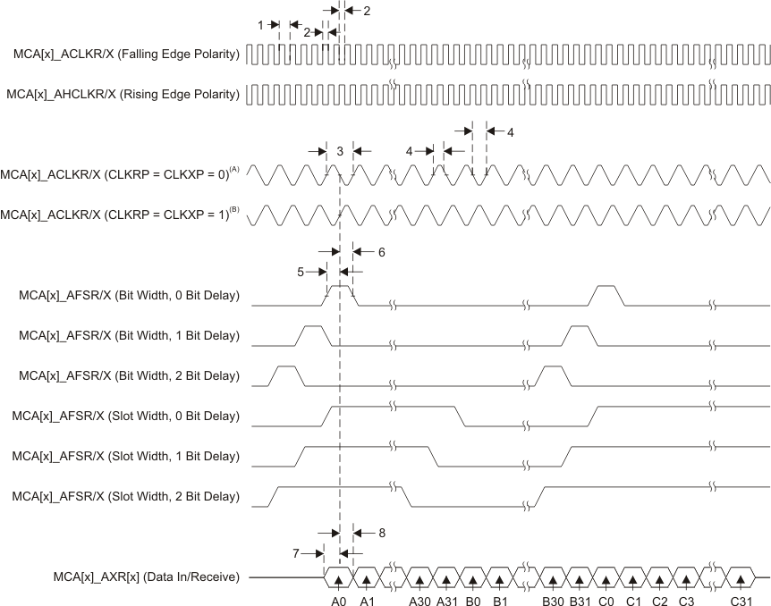
Table 7-79 Switching Characteristics Over Recommended Operating Conditions for McASP(1)
(see Figure 7-82)| NO. | PARAMETER | OPP100/120/166 | UNIT | |||
|---|---|---|---|---|---|---|
| MIN | MAX | |||||
| 9 | tc(AHCLKRX) | Cycle time, MCA[X]_AHCLKR/X | 20(2) | ns | ||
| 10 | tw(AHCLKRX) | Pulse duration, MCA[X]_AHCLKR/X high or low | 0.5P - 2.5(3) | ns | ||
| 11 | tc(ACLKRX) | Cycle time, MCA[X]_ACLKR/X | 20 | ns | ||
| 12 | tw(ACLKRX) | Pulse duration, MCA[X]_ACLKR/X high or low | 0.5P - 2.5(3) | ns | ||
| 13 | td(ACLKRX-AFSRX) | Delay time, MCA[X]_ACLKR/X transmit edge to MCA[X]_AFSR/X output valid | ACLKR/X int | -2 | 5 | ns |
| ACLKR/X ext in | 1 | 11.5 | ||||
| Delay time, MCA[X]_ACLKR/X transmit edge to MCA[X]_AFSR/X output valid with Pad Loopback | ACLKR/X ext out | 1 | 11.5 | |||
| 14 | td(ACLKX-AXR) | Delay time, MCA[X]_ACLKX transmit edge to MCA[X]_AXR output valid | ACLKX int | -2 | 5 | ns |
| ACLKX ext in | 1 | 11.5 | ||||
| Delay time, MCA[X]_ACLKX transmit edge to MCA[X]_AXR output valid with Pad Loopback | ACLKX ext out | 1 | 11.5 | |||
| 15 | tdis(ACLKX-AXR) | Disable time, MCA[X]_ACLKX transmit edge to MCA[X]_AXR output high impedance | ACLKX int | -2 | 5 | ns |
| ACLKX ext in | 1 | 11.5 | ||||
| Disable time, MCA[X]_ACLKX transmit edge to MCA[X]_AXR output high impedance with Pad Loopback | ACLKX ext out | 1 | 11.5 | |||
ACLKR external input: ACLKRCTL.CLKRM=0, PDIR.ACLKR=0
ACLKR external output: ACLKRCTL.CLKRM=0, PDIR.ACLKR=1
ACLKX internal: ACLKXCTL.CLKXM=1, PDIR.ACLKX = 1
ACLKX external input: ACLKXCTL.CLKXM=0, PDIR.ACLKX=0
ACLKX external output: ACLKXCTL.CLKXM=0, PDIR.ACLKX=1

7.15 Multichannel Buffered Serial Port (McBSP)
The McBSP provides these functions:
- Full-duplex communication
- Double-buffered data registers, which allow a continuous data stream
- Independent framing and clocking for receive and transmit
- Direct interface to industry-standard codecs, analog interface chips (AICs), and other serially connected analog-to-digital (A/D) and digital-to-analog (D/A) devices
- Supports TDM, I2S, and similar formats
- External shift clock or an internal, programmable frequency shift clock for data transfer
- 5KB Tx and Rx buffer
- Supports three interrupt and two DMA requests.
The McBSP module may support two types of data transfer at the system level:
- The full-cycle mode, for which one clock period is used to transfer the data, generated on one edge and captured on the same edge (one clock period later).
- The half-cycle mode, for which one half clock period is used to transfer the data, generated on one edge and captured on the opposite edge (one half clock period later). Note that a new data is generated only every clock period, which secures the required hold time. The interface clock (CLKX/CLKR) activation edge (data/frame sync capture and generation) has to be configured accordingly with the external peripheral (activation edge capability) and the type of data transfer required at the system level.
For more detailed information on the McBSP peripheral, see the Multichannel Buffered Serial Port (McBSP) chapter of the AM387x Sitara™ ARM Processors Technical Reference Manual (Literature Number: SPRUGZ7).
The following sections describe the timing characteristics for applications in normal mode (that is, the McBSP connected to one peripheral) and TDM applications in multipoint mode.
7.15.1 McBSP Peripheral Register Descriptions
Table 7-80 McBSP Registers(1)
| HEX ADDRESS | ACRONYM | REGISTER NAME |
|---|---|---|
| 0x4700 0000 | REVNB | Revision Number Register |
| 0x4700 0010 | SYSCONFIG_REG | System Configuration Register |
| 0x4700 0020 | EOI | End of Interrupt Register |
| 0x4700 0024 | IRQSTATUS_RAW | Interrupt Status Raw Register |
| 0x4700 0028 | IRQSTATUS | Interrupt Status Register |
| 0x4700 002C | IRQENABLE_SET | Interrupt Enable Set Register |
| 0x4700 0030 | IRQENABLE_CLR | Interrupt Enable Clear Register |
| 0x4700 0034 | DMARXENABLE_SET | DMA Rx Enable Set Register |
| 0x4700 0038 | DMATXENABLE_SET | DMA Tx Enable Set Register |
| 0x4700 003C | DMARXENABLE_CLR | DMA Rx Enable Clear Register |
| 0x4700 0040 | DMATXENABLE_CLR | DMA Tx Enable Clear Register |
| 0x4700 0048 | DMARXWAKE_EN | DMA Rx Wake Enable Register |
| 0x4700 004C | DMATXWAKE_EN | DMA Tx Wake Enable Register |
| 0x4700 0100 | DRR_REG | McBSP data receive |
| 0x4700 0108 | DXR_REG | McBSP data transmit |
| 0x4700 0110 | SPCR2_REG | McBSP serial port control 2 |
| 0x4700 0114 | SPCR1_REG | McBSP serial port control 1 |
| 0x4700 0118 | RCR2_REG | McBSP receive control 2 |
| 0x4700 011C | RCR1_REG | McBSP receive control 1 |
| 0x4700 0120 | XCR2_REG | McBSP transmit control 2 |
| 0x4700 0124 | XCR1_REG | McBSP transmit control 1 |
| 0x4700 0128 | SRGR2_REG | McBSP sample rate generator 2 |
| 0x4700 012C | SRGR1_REG | McBSP sample rate generator 1 |
| 0x4700 0130 | MCR2_REG | McBSP multichannel 2 |
| 0x4700 0134 | MCR1_REG | McBSP multichannel 1 |
| 0x4700 0138 | RCERA_REG | McBSP receive channel enable partition A |
| 0x4700 013C | RCERB_REG | McBSP receive channel enable partition B |
| 0x4700 0140 | XCERA_REG | McBSP transmit channel enable partition A |
| 0x4700 0144 | XCERB_REG | McBSP transmit channel enable partition B |
| 0x4700 0148 | PCR_REG | McBSP pin control |
| 0x4700 014C | RCERC_REG | McBSP receive channel enable partition C |
| 0x4700 0150 | RCERD_REG | McBSP receive channel enable partition D |
| 0x4700 0154 | XCERC_REG | McBSP transmit channel enable partition C |
| 0x4700 0158 | XCERD_REG | McBSP transmit channel enable partition D |
| 0x4700 015C | RCERE_REG | McBSP receive channel enable partition E |
| 0x4700 0160 | RCERF_REG | McBSP receive channel enable partition F |
| 0x4700 0164 | XCERE_REG | McBSP transmit channel enable partition E |
| 0x4700 0168 | XCERF_REG | McBSP transmit channel enable partition F |
| 0x4700 016C | RCERG_REG | McBSP receive channel enable partition G |
| 0x4700 0170 | RCERH_REG | McBSP receive channel enable partition H |
| 0x4700 0174 | XCERG_REG | McBSP transmit channel enable partition G |
| 0x4700 0178 | XCERH_REG | McBSP transmit channel enable partition H |
| 0x4700 017C | REV_REG | McBSP revision number |
| 0x4700 0180 | RINTCLR_REG | McBSP receive interrupt clear |
| 0x4700 0184 | XINTCLR_REG | McBSP transmit interrupt clear |
| 0x4700 0188 | ROVFLCLR_REG | McBSP receive overflow interrupt clear |
| 0x4700 018C | SYSCONFIG_REG | McBSP system configuration |
| 0x4700 0190 | THRSH2_REG | McBSP transmit buffer threshold (DMA or IRQ trigger) |
| 0x4700 0194 | THRSH1_REG | McBSP receive buffer threshold (DMA or IRQ trigger) |
| 0x4700 01A0 | IRQSTATATUS | McBSP interrupt status (OCP compliant IRQ line) |
| 0x4700 01A4 | IRQENABLE | McBSP interrupt enable (OCP compliant IRQ line) |
| 0x4700 01A8 | WAKEUPEN | McBSP wakeup enable |
| 0x4700 01AC | XCCR_REG | McBSP transmit configuration control |
| 0x4700 01B0 | RCCR_REG | McBSP receive configuration control |
| 0x4700 01B4 | XBUFFSTAT_REG | McBSP transmit buffer status |
| 0x4700 01B8 | RBUFFSTAT_REG | McBSP receive buffer status |
| 0x4700 01C0 | STATUS_REG | McBSP status |
7.15.2 McBSP Electrical Data/Timing
Table 7-81 Timing Requirements for McBSP - Master Mode(1)
(see Figure 7-83)| NO. | OPP100/120/166 | UNIT | |||
|---|---|---|---|---|---|
| MIN | MAX | ||||
| 6 | tsu(DRV-CLKAE) | Setup time, MCB_DR valid before MCB_CLK active edge(2) | 3.5 | ns | |
| 7 | th(CLKAE-DRV) | Hold time, MCB_DR valid after MCB_CLK active edge(2) | 3.5 | ns | |
Table 7-82 Switching Characteristics Over Recommended Operating Conditions for McBSP - Master Mode(1)
(see Figure 7-83)| NO. | PARAMETER | OPP100/120/166 | UNIT | ||
|---|---|---|---|---|---|
| MIN | MAX | ||||
| 1 | tc(CLK) | Cycle time, output MCB_CLK period(2) | 20.83 | ns | |
| 2 | tw(CLKL) | Pulse duration, output MCB_CLK low(2) | 0.5*P - 1(3) | ns | |
| 3 | tw(CLKH) | Pulse duration, output MCB_CLK high(2) | 0.5*P - 1(3) | ns | |
| 4 | td(CLKAE-FSV) | Delay time, output MCB_CLK active edge to output MCB_FS valid(2)(4) | 0.3 | 9.4 | ns |
| 5 | td(CLKXAE-DXV) | Delay time, output MCB_CLKX active edge to output MCB_DX valid | 0.3 | 9.4 | ns |

McBSP in 6-pin mode: DX and DR as data pins; CLKX, CLKR, FSX and FSR as control pins.
McBSP in 4-pin mode: DX and DR as data pins; CLKX and FSX pins as control pins. The CLKX and FSX pins are internally looped back via software configuration, respectively to the CLKR and FSR internal signals for data receive.
Table 7-83 Timing Requirements for McBSP - Slave Mode(1)
(see Figure 7-84)| NO. | OPP100/120/166 | UNIT | |||
|---|---|---|---|---|---|
| MIN | MAX | ||||
| 1 | tc(CLK) | Cycle time, MCB_CLK period(2) | 20.83 | ns | |
| 2 | tw(CLKL) | Pulse duration, MCB_CLK low(2) | 0.5*P - 1(3) | ns | |
| 3 | tw(CLKH) | Pulse duration, MCB_CLK high(2) | 0.5*P - 1(3) | ns | |
| 4 | tsu(FSV-CLKAE) | Setup time, MCB_FS valid before MCB_CLK active edge(2)(4) | 3.8 | ns | |
| 5 | th(CLKAE-FSV) | Hold time, MCB_FS valid after MCB_CLK active edge(2)(4) | 0.5 | ns | |
| 7 | tsu(DRV-CLKAE) | Setup time, MCB_DR valid before MCB_CLK active edge(2) | 3.8 | ns | |
| 8 | th(CLKAE-DRV) | Hold time, MCB_DR valid after MCB_CLK active edge(2) | 0.5 | ns | |
Table 7-84 Switching Characteristics Over Recommended Operating Conditions for McBSP - Slave Mode(1)
(see Figure 7-84)| NO. | PARAMETER | OPP100/120/166 | UNIT | ||
|---|---|---|---|---|---|
| MIN | MAX | ||||
| 6 | td(CLKXAE-DXV) | Delay time, input MCB_CLKx active edge to output MCB_DX valid | 0.5 | 12.5 | ns |

McBSP in 6-pin mode: DX and DR as data pins; CLKX, CLKR, FSX and FSR as control pins.
McBSP in 4-pin mode: DX and DR as data pins; CLKX and FSX pins as control pins. The CLKX and FSX pins are internally looped back via software configuration, respectively to the CLKR and FSR internal signals for data receive.
7.16 MultiMedia Card/Secure Digital/Secure Digital Input Output (MMC/SD/SDIO)
The device includes 3 MMC/SD/SDIO Controllers which are compliant with MMC V4.3, Secure Digital Part 1 Physical Layer Specification V2.00 and Secure Digital Input Output (SDIO) V2.00 specifications.
The device MMC/SD/SDIO Controller has the following features:
- MultiMedia card (MMC)
- Secure Digital (SD) memory card
- MMC/SD protocol support
- SDIO protocol support
- Programmable clock frequency
- 1024 byte read/write FIFO to lower system overhead
- Slave EDMA transfer capability
- SD High capacity support
7.16.1 MMC/SD/SDIO Peripheral Register Descriptions
Table 7-85 MMC/SD/SDIO Registers(1)
| MMC/SD/SDIO0 HEX ADDRESS |
MMC/SD/SDIO1 HEX ADDRESS |
MMC/SD/SDIO2 HEX ADDRESS |
ACRONYM | REGISTER NAME |
|---|---|---|---|---|
| 0x4806 0000 | 0x481D 8000 | 0x4781 0000 | MMCHS_HL_REV | IP Revision Identifier |
| 0x4806 0004 | 0x481D 8004 | 0x4781 0004 | MMCHS_HL_HWINFO | Hardware Configuration |
| 0x4806 0010 | 0x481D 8010 | 0x4781 0010 | MMCHS_HL_SYSCONFIG | Clock Management Configuration |
| 0x4806 0110 | 0x481D 8110 | 0x4781 0110 | MMCHS_SYSCONFIG | System Configuration |
| 0x4806 0114 | 0x481D 8114 | 0x4781 0114 | MMCHS_SYSSTATUS | System Status |
| 0x4806 0124 | 0x481D 8124 | 0x4781 0124 | MMCHS_CSRE | Card status response error |
| 0x4806 0128 | 0x481D 8128 | 0x4781 0128 | MMCHS_SYSTEST | System Test |
| 0x4806 012C | 0x481D 812C | 0x4781 012C | MMCHS_CON | Configuration |
| 0x4806 0130 | 0x481D 8130 | 0x4781 0130 | MMCHS_PWCNT | Power counter |
| 0x4806 0200 | 0x481D 8200 | 0x4781 0200 | MMCHS_SDMASA | SDMA System address: |
| 0x4806 0204 | 0x481D 8204 | 0x4781 0204 | MMCHS_BLK | Transfer Length Configuration |
| 0x4806 0208 | 0x481D 8208 | 0x4781 0208 | MMCHS_ARG | Command argument |
| 0x4806 020C | 0x481D 820C | 0x4781 020C | MMCHS_CMD | Command and transfer mode |
| 0x4806 0210 | 0x481D 8210 | 0x4781 0210 | MMCHS_RSP10 | Command Response 0 and 1 |
| 0x4806 0214 | 0x481D 8214 | 0x4781 0214 | MMCHS_RSP32 | Command Response 2 and 3 |
| 0x4806 0218 | 0x481D 8218 | 0x4781 0218 | MMCHS_RSP54 | Command Response 4 and 5 |
| 0x4806 021C | 0x481D 821C | 0x4781 021C | MMCHS_RSP76 | Command Response 6 and 7 |
| 0x4806 0220 | 0x481D 8220 | 0x4781 0220 | MMCHS_DATA | Data |
| 0x4806 0224 | 0x481D 8224 | 0x4781 0224 | MMCHS_PSTATE | Present state |
| 0x4806 0228 | 0x481D 8228 | 0x4781 0228 | MMCHS_HCTL | Host Control |
| 0x4806 022C | 0x481D 822C | 0x4781 022C | MMCHS_SYSCTL | SD system control |
| 0x4806 0230 | 0x481D 8230 | 0x4781 0230 | MMCHS_STAT | Interrupt status |
| 0x4806 0234 | 0x481D 8234 | 0x4781 0234 | MMCHS_IE | Interrupt SD enable |
| 0x4806 0238 | 0x481D 8238 | 0x4781 0238 | MMCHS_ISE | Interrupt Signal Enable |
| 0x4806 023C | 0x481D 823C | 0x4781 023C | MMCHS_AC12 | Auto CMD12 Error Status |
| 0x4806 0240 | 0x481D 8240 | 0x4781 0240 | MMCHS_CAPA | Capabilities |
| 0x4806 0248 | 0x481D 8248 | 0x4781 0248 | MMCHS_CUR_CAPA | Maximum current capabilities |
| 0x4806 0250 | 0x481D 8250 | 0x4781 0250 | MMCHS_FE | Force Event |
| 0x4806 0254 | 0x481D 8254 | 0x4781 0254 | MMCHS_ADMAES | ADMA Error Status |
| 0x4806 0258 | 0x481D 8258 | 0x4781 0258 | MMCHS_ADMASAL | ADMA System address Low bits |
| 0x4806 025C | 0x481D 825C | 0x4781 025C | MMCHS_ADMASAH | ADMA System address High bits |
| 0x4806 02FC | 0x481D 82FC | 0x4781 02FC | MMCHS_REV | Versions |
7.16.2 MMC/SD/SDIO Electrical Data/Timing
Table 7-86 Timing Requirements for MMC/SD/SDIO
(see Figure 7-86, Figure 7-88)| NO. | OPP100/120/166 | UNIT | ||||
|---|---|---|---|---|---|---|
| ALL MODES | ||||||
| MIN | MAX | |||||
| 1 | tsu(CMDV-CLKH) | Setup time, SD_CMD valid before SD_CLK rising clock edge | 4.1 | ns | ||
| 2 | th(CLKH-CMDV) | Hold time, SD_CMD valid after SD_CLK rising clock edge | SD1 | 1.9 | ns | |
| SD0, SD2 | 2.9 | |||||
| 3 | tsu(DATV-CLKH) | Setup time, SD_DATx valid before SD_CLK rising clock edge | 4.1 | ns | ||
| 4 | th(CLKH-DATV) | Hold time, SD_DATx valid after SD_CLK rising clock edge | SD1 | 1.9 | ns | |
| SD0, SD2 | 2.9 | |||||
Table 7-87 Switching Characteristics Over Recommended Operating Conditions for MMC/SD/SDIO
(see Figure 7-85 through Figure 7-88)| NO. | PARAMETER | OPP100/120/166 | UNIT | ||||
|---|---|---|---|---|---|---|---|
| MODES | |||||||
| 3.3 V STD 1.8 V SDR12 |
3.3 V HS 1.8 V SDR25 |
||||||
| MIN | MAX | MIN | MAX | ||||
| 7 | fop(CLK) | Operating frequency, SD_CLK | 24 | 48 | MHz | ||
| tc(CLK) | Operating period: SD_CLK | 41.7 | 20.8 | ns | |||
| 8 | fop(CLKID) | Identification mode frequency, SD_CLK | 400 | 400 | kHz | ||
| tc(CLKID) | Identification mode period: SD_CLK | 2500.0 | 2500.0 | ns | |||
| 9 | tw(CLKL) | Pulse duration, SD_CLK low | 0.5*P(1) | 0.5*P(1) | ns | ||
| 10 | tw(CLKH) | Pulse duration, SD_CLK high | 0.5*P(1) | 0.5*P(1) | ns | ||
| 11 | tr(CLK) | Rise time, All Signals (10% to 90%) | 2.2 | 2.2 | ns | ||
| 12 | tf(CLK) | Fall time, All Signals (10% to 90%) | 2.2 | 2.2 | ns | ||
| 13 | td(CLKL-CMD) | Delay time, SD_CLK rising clock edge to SD_CMD transition | 1.5 | 10 | 1.5 | 10 | ns |
| 14 | td(CLKL-DAT) | Delay time, SD_CLK rising clock edge to SD_DATx transition | 1.5 | 10 | 1.5 | 10 | ns |
 Figure 7-85 MMC/SD/SDIO Host Command Timing
 Figure 7-86 MMC/SD/SDIO Card Response Timing
 Figure 7-87 MMC/SD/SDIO Host Write Timing
 Figure 7-88 MMC/SD/SDIO Host Read and Card CRC Status Timing
7.17 Peripheral Component Interconnect Express (PCIe)
The device supports connections to PCIe-compliant devices via the integrated PCIe master/slave bus interface. The PCIe module is comprised of a dual-mode PCIe core and a SerDes PHY. The device implements a single one-lane PCIe 2.0 (5.0 GT/s) Endpoint/Root Complex port.
The device PCIe supports the following features:
- Supports Gen1/Gen2 in x1 or x2 mode
- One port with one 5 GT/s lane
- Single virtual channel (VC), single traffic class (TC)
- Single function in end-point mode
- Automatic width and speed negotiation and lane reversal
- Max payload: 128 byte outbound, 256 byte inbound
- Automatic credit management
- ECRC generation and checking
- Configurable BAR filtering
- Supports PCIe messages
- Legacy interrupt reception (RC) and generation (EP)
- MSI generation and reception
- PCI device power management, except D3 cold with vaux
- Active state power management state L0 and L1.
For more detailed information on the PCIe port peripheral module, see the PCI Express (PCIe) Module chapter of the AM387x Sitara™ ARM Processors Technical Reference Manual (Literature Number: SPRUGZ7).
The PCIe peripheral on the device conforms to the PCI-Express Base 2.0 Specification.
7.17.1 PCIe Peripheral Register Descriptions
Table 7-88 PCIe Registers
| HEX ADDRESS | ACRONYM | REGISTER NAME |
|---|---|---|
| 0x5100 0000 | PID | Peripheral Version and ID |
| 0x5100 0004 | CMD_STATUS | Command Status |
| 0x5100 0008 | CFG_SETUP | Config Transaction Setup |
| 0x5100 000C | IOBASE | IO TLP Base |
| 0x5100 0010 | TLPCFG | TLP Attribute Configuration |
| 0x5100 0014 | RSTCMD | Reset Command and Status |
| 0x5100 0020 | PMCMD | Power Management Command |
| 0x5100 0024 | PMCFG | Power Management Configuration |
| 0x5100 0028 | ACT_STATUS | Activity Status |
| 0x5100 0030 | OB_SIZE | Outbound Size |
| 0x5100 0034 | DIAG_CTRL | Diagnostic Control |
| 0x5100 0038 | ENDIAN | Endian Mode |
| 0x5100 003C | PRIORITY | CBA Transaction Priority |
| 0x5100 0050 | IRQ_EOI | End of Interrupt |
| 0x5100 0054 | MSI_IRQ | MSI Interrupt IRQ |
| 0x5100 0064 | EP_IRQ_SET | Endpoint Interrupt Request Set |
| 0x5100 0068 | EP_IRQ_CLR | Endpoint Interrupt Request Clear |
| 0x5100 006C | EP_IRQ_STATUS | Endpoint Interrupt Status |
| 0x5100 0070 | GPRO | General Purpose 0 |
| 0x5100 0074 | GPR1 | General Purpose 1 |
| 0x5100 0078 | GPR2 | General Purpose 2 |
| 0x5100 007C | GPR3 | General Purpose 3 |
| 0x5100 0100 | MSI0_IRQ_STATUS_RAW | MSI 0 Interrupt Raw Status |
| 0x5100 0104 | MSI0_IRQ_STATUS | MSI 0 Interrupt Enabled Status |
| 0x5100 0108 | MSI0_IRQ_ENABLE_SET | MSI 0 Interrupt Enable Set |
| 0x5100 010C | MSI0_IRQ_ENABLE_CLR | MSI 0 Interrupt Enable Clear |
| 0x5100 0180 | IRQ_STATUS_RAW | Raw Interrupt Status |
| 0x5100 0184 | IRQ_STATUS | Interrupt Enabled Status |
| 0x5100 0188 | IRQ_ENABLE_SET | Interrupt Enable Set |
| 0x5100 018C | IRQ_ENABLE_CLR | Interrupt Enable Clear |
| 0x5100 01C0 | ERR_IRQ_STATUS_RAW | Raw ERR Interrupt Status |
| 0x5100 01C4 | ERR_IRQ_STATUS | ERR Interrupt Enabled Status |
| 0x5100 01C8 | ERR_IRQ_ENABLE_SET | ERR Interrupt Enable Set |
| 0x5100 01CC | ERR_IRQ_ENABLE_CLR | ERR Interrupt Enable Clear |
| 0x5100 01D0 | PMRST_IRQ_STATUS_RAW | Power Management and Reset Interrupt Status |
| 0x5100 01D4 | PMRST_IRQ_STATUS | Power Management and Reset Interrupt Enabled Status |
| 0x5100 01D8 | PMRST_ENABLE_SET | Power Management and Reset Interrupt Enable Set |
| 0x5100 01DC | PMRST_ENABLE_CLR | Power Management and Reset Interrupt Enable Clear |
| 0x5100 0200 | OB_OFFSET_INDEXn | Outbound Translation Region N Offset Low and Index |
| 0x5100 0204 | OB_OFFSETn_HI | Outbound Translation Region N Offset High |
| 0x5100 0300 | IB_BAR0 | Inbound Translation Bar Match 0 |
| 0x5100 0304 | IB_START0_LO | Inbound Translation 0 Start Address Low |
| 0x5100 0308 | IB_START0_HI | Inbound Translation 0 Start Address High |
| 0x5100 030C | IB_OFFSET0 | Inbound Translation 0 Address Offset |
| 0x5100 0310 | IB_BAR1 | Inbound Translation Bar Match 1 |
| 0x5100 0314 | IB_START1_LO | Inbound Translation 1 Start Address Low |
| 0x5100 0318 | IB_START1_HI | Inbound Translation 1 Start Address High |
| 0x5100 031C | IB_OFFSET1 | Inbound Translation 1 Address Offset |
| 0x5100 0320 | IB_BAR2 | Inbound Translation Bar Match 2 |
| 0x5100 0324 | IB_START2_LO | Inbound Translation 2 Start Address Low |
| 0x5100 0328 | IB_START2_HI | Inbound Translation 2 Start Address High |
| 0x5100 032C | IB_OFFSET2 | Inbound Translation 2 Address Offset |
| 0x5100 0330 | IB_BAR3 | Inbound Translation Bar Match 3 |
| 0x5100 0334 | IB_START3_LO | Inbound Translation 3 Start Address Low |
| 0x5100 0338 | IB_START3_HI | Inbound Translation 3 Start Address High |
| 0x5100 033C | IB_OFFSET3 | Inbound Translation 3 Address Offset |
| 0x5100 0380 | PCS_CFG0 | PCS Configuration 0 |
| 0x5100 0384 | PCS_CFG1 | PCS Configuration 1 |
| 0x5100 0388 | PCS_STATUS | PCS Status |
| 0x5100 038C | SERDES_STATUS | SerDes Status |
| 0x5100 0390 | SERDES_RXCFG0 | SerDes Receive Configuration 0 Register |
| 0x5100 0394 | SERDES_RXCFG1 | SerDes Receive Configuration 1 Register |
| 0x5100 0398 | SERDES_RXCFG2 | SerDes Receive Configuration 2 Register |
| 0x5100 039C | SERDES_RXCFG3 | SerDes Receive Configuration 3 Register |
| 0x5100 03A0 | SERDES_RXCFG4 | SerDes Receive Configuration 4 Register |
| 0x5100 03A4 | SERDES_TXCFG0 | SerDes Transmit Configuration 0 Register |
| 0x5100 03A8 | SERDES_TXCFG1 | SerDes Transmit Configuration 1 Register |
| 0x5100 03AC | SERDES_TXCFG2 | SerDes Transmit Configuration 2 Register |
| 0x5100 03B0 | SERDES_TXCFG3 | SerDes Transmit Configuration 3 Register |
| 0x5100 03B4 | SERDES_TXCFG4 | SerDes Transmit Configuration 4 Register |
Table 7-89 Configuration Registers Type 0 Summary
| HEX ADDRESS | ACRONYM | NAME |
|---|---|---|
| 5100_1000 | VENDOR_DEVICE_ID | Vendor Device ID Register |
| 5100_1004 | STATUS_COMMAND | Status and Command Register |
| 5100_1008 | CLASSCODE_REVID | Class Code and Revision Register |
| 5100_100C | BIST_HEADER | BIST, Header Type, Latency Time, and Cache Line Size register |
| 5100_1010 | BAR0 (64/-32-Bit Mode) | Base Address Register 0 |
| 5100_1014 | BAR1 (32-Bit Mode) | Base Address Register 1 |
| BAR1 (64-Bit Mode) | Base Address Register 1 (64-bit BAR0) | |
| 5100_1018 | BAR2 (64/-32-Bit Mode) | Base Address Register 2 |
| 5100_101C | BAR3 (32-Bit Mode) | Base Address Register 3 |
| BAR3 (64-Bit Mode) | Base Address Register 3 (64-bit BAR2) | |
| 5100_1020 | BAR4 (64/-32-Bit Mode) | Base Address Register 4 |
| 5100_1024 | BAR5 (32-Bit Mode) | Base Address Register 5 |
| BAR5 (64-Bit Mode) | Base Address Register 5 (64-bit BAR4) | |
| 5100_1028 | CARDBUS | CardBus CIS Pointer Register |
| 5100_102C | SUBSYS_VNDR_ID | Subsystem and Subsystem Vendor ID Register |
| 5100_1030 | EXPNSN_ROM | Expansion ROM Base Address Register |
| 5100_1034 | CAP_PTR | Capabilities Pointer Register |
| 5100_103C | INT_PIN | Interrupt Pin Register |
Table 7-90 Configuration Registers Type 1 Summary
| HEX ADDRESS | ACRONYM | NAME |
|---|---|---|
| 5100_1000 | VENDOR_DEVICE_ID | Vendor Device ID Register |
| 5100_1004 | STATUS_COMMAND | Status and Command Register |
| 5100_1008 | CLASSCODE_REVID | Class Code and Revision Register |
| 5100_100C | BIST_HEADER | BIST, Header Type, Latency Time, and Cache Line Size register |
| 5100_1010 | BAR0 (64/-32-Bit Mode) | Base Address Register 0 (64/32-bit mode) |
| 5100_1014 | BAR1 (32-Bit Mode) | Base Address Register 1 (32-bit mode) |
| BAR1 (64-Bit Mode) | Base Address Register 1 (64-bit BAR0) | |
| 5100_1018 | BUSNUM | Latency Timer and Bus Number Register |
| 5100_101C | SECSTAT | Secondary Status and I/O Base/Limit Register |
| 5100_1020 | MEMSPACE | Memory Limit and Base Register |
| 5100_1024 | PREFETCH_MEM | Prefetchable Memory Limit and Base Register |
| 5100_1028 | PREFETCH_BASE | Prefetchable Memory Base Upper 32-bits Register |
| 5100_102C | PREFETCH_LIMIT | Prefetchable Limit Upper 32-bits Register |
| 5100_1030 | IOSPACE | I/O Base and Limit Upper 16-bits Register |
| 5100_1034 | CAP_PTR | Capabilities Pointer Register |
| 5100_1038 | EXPNSN_ROM | Expansion ROM Base Address Register |
| 5100_103C | BRIDGE_INT | Bridge Control Register |
Table 7-91 Power Management Capability Register Summary
| HEX ADDRESS | ACRONYM | NAME |
|---|---|---|
| 5100_1040 | PMCAP | Power Management Capability Register |
| 5100_1044 | PM_CTL_STAT | Power Management Control and Status Register |
Table 7-92 Message Signaled Interrupts (MSI) Register Summary
| HEX ADDRESS | ACRONYM | NAME |
|---|---|---|
| 5100_1050 | MSI_CAP | MSI Capabilities Register |
| 5100_1054 | MSI_LOW32 | MSI Lower 32 bits Register |
| 5100_1058 | MSI_UP32 | MSI Upper 32 bits Register |
| 5100_105C | MSI_DATA | MSI Data Register |
Table 7-93 PCI-Express Capabilities Register Summary
| HEX ADDRESS | ACRONYM | NAME |
|---|---|---|
| 5100_1070 | PCIES_CAP | PCI-Express Capabilities Register |
| 5100_1074 | DEVICE_CAP | Device Capabilities Register |
| 5100_1078 | DEV_STAT_CTRL | Device Status and Control Register |
| 5100_107C | LINK_CAP | Link Capabilities Register |
| 5100_1080 | LINK_STAT_CTRL | Link Status and Control Register |
| 5100_1084 | SLOT_CAP | Slot Capabilities Register (RC Mode Only) |
| 5100_1088 | SLOT_STAT_CTRL | Slot Status and Control Register (RC Mode Only) |
| 5100_108C | ROOT_CTRL_CAP | Root Control and Capabilities Register (RC Mode Only) |
| 5100_1090 | ROOT_STATUS | Root Status and Control Register (RC Mode Only) |
| 5100_1094 | DEV_CAP2 | Device Capabilities 2 Register |
| 5100_1098 | DEV_STAT_CTRL2 | Device Status and Control 2 Register |
| 5100_10A0 | LINK_CTRL2 | Link Control 2 Register |
Table 7-94 PCI-Express Extended Capabilities Register Summary
| HEX ADDRESS | ACRONYM | NAME |
|---|---|---|
| 5100_1100 | PCIE_EXTCAP | PCI-Express Extended Capabilities Header Register |
| 5100_1104 | PCIE_UNCERR | PCI-Express Uncorrectable Error Status Register |
| 5100_1108 | PCIE_UNCERR_MASK | PCI-Express Uncorrectable Error Mask Register |
| 5100_110C | PCIE_UNCERR_SVRTY | PCI-Express Uncorrectable Error Severity Register |
| 5100_1110 | PCIE_CERR | PCI-Express Correctable Error Status Register |
| 5100_1114 | PCIE_CERR_MASK | PCI-Express Correctable Error Mask Register |
| 5100_1118 | PCIE_ACCR | PCI-Express Advanced Capabilities and Control Register |
| 5100_111C | HDR_LOG0 | Header Log 0 Register |
| 5100_1120 | HDR_LOG1 | Header Log 1 Register |
| 5100_1124 | HDR_LOG2 | Header Log 2 Register |
| 5100_1128 | HDR_LOG3 | Header Log 3 Register |
| 5100_112C | RC_ERR_CMD | Root Error Command Register |
| 5100_1130 | RC_ERR_ST | Root Error Status Register |
| 5100_1134 | ERR_SRC_ID | Error Source Identification Register |
Table 7-95 Port Logic Register Summary
| HEX ADDRESS | ACRONYM | NAME |
|---|---|---|
| 5100_1700 | PL_ACKTIMER | Ack Latency Time and Replay Timer Register |
| 5100_1704 | PL_OMSG | Other Message Register |
| 5100_1708 | PL_FORCE_LINK | Port Force Link Register |
| 5100_170C | ACK_FREQ | Ack Frequency Register |
| 5100_1710 | PL_LINK_CTRL | Port Link Control Register |
| 5100_1714 | LANE_SKEW | Lane Skew Register |
| 5100_1718 | SYM_NUM | Symbol Number Register |
| 5100_171C | SYMTIMER_FLTMASK | Symbol Timer and Filter Mask Register |
| 5100_1720 | FLT_MASK2 | Filter Mask 2 Register |
| 5100_1728 | DEBUG0 | Debug 0 Register |
| 5100_172C | DEBUG1 | Debug 1 Register |
| 5100_180C | PL_GEN2 | Gen2 Register |
7.17.2 PCIe Electrical Data/Timing
Texas Instruments (TI) has performed the simulation and system characterization to ensure that the PCIe peripheral meets all AC timing specifications as required by the PCI-Express Base 2.0 Specification. Therefore, the AC timing specifications are not reproduced here. For more information on the AC timing specifications, see Sections 4.3.3.5 and 4.3.4.4 of the PCI-Express Base 2.0 Specification.
7.17.3 PCIe Design and Layout Guidelines
7.17.3.1 Clock Source
A standard 100-MHz PCIe differential clock source must be used for PCIe operation (for more details, see Section 6.4.2, SERDES CLKN/P Input Clock).
7.17.3.2 PCIe Connections and Interface Compliance
The PCIe interface on the device is compliant with the PCI-Express Base 2.0 Specification. Refer to the PCIe specifications for all connections that are described in it. For coupling capacitor selection, see Section 7.17.3.2.1, Coupling Capacitors.
The use of PCIe-compatible bridges and switches is allowed for interfacing with more than one other processor or PCIe device.
7.17.3.2.1 Coupling Capacitors
AC coupling capacitors are required on the transmit data pair. Table 7-96 shows the requirements for these capacitors.
Table 7-96 AC Coupling Capacitors Requirements
| PARAMETER | MIN | TYP | MAX | UNIT |
|---|---|---|---|---|
| PCIe AC coupling capacitor value | 75 | 200 | nF | |
| PCIe AC coupling capacitor package size(1) | 0402 | 0603 | EIA(2) |
7.17.3.2.2 Polarity Inversion
The PCIe specification requires polarity inversion support. This means, for layout purposes, polarity is unimportant because each signal can change its polarity on-die inside the chip. This means polarity within a lane is unimportant for layout.
7.17.3.3 Nonstandard PCIe Connections
The following sections contain suggestions for any PCIe connection that is not described in the official PCIe specification, such as an on-board device-to-device connection, or device-to-other PCIe-compliant processor connection.
7.17.3.3.1 PCB Stackup Specifications
Table 7-97 shows the stackup and feature sizes required for these types of PCIe connections.
Table 7-97 PCIe PCB Stackup Specifications
| PARAMETER | MIN | TYP | MAX | UNIT |
|---|---|---|---|---|
| PCB Routing/Plane Layers | 4 | 6 | - | Layers |
| Signal Routing Layers | 2 | 3 | - | Layers |
| Number of ground plane cuts allowed within PCIe routing region | - | - | 0 | Cuts |
| Number of layers between PCIe routing area and reference plane(1) | - | - | 0 | Layers |
| PCB Routing clearance | - | 4 | - | Mils |
| PCB Trace width(2) | - | 4 | - | Mils |
| PCB BGA escape via pad size | - | 20 | - | Mils |
| PCB BGA escape via hole size | - | 10 | Mils | |
| MPU BGA pad size(3)(4) | 0.4 | mm |
7.17.3.3.2 Routing Specifications
The PCIe data signal traces must be routed to achieve 100 Ω (±20%) differential impedance and 60 Ω (±15%) single-ended impedance. The single-ended impedance is required because differential signals are extremely difficult to closely couple on PCBs and, therefore, single-ended impedance becomes important. These requirements are the same as those recommended in the PCIe Motherboard Checklist 1.0 document, available from PCI-SIG.
These impedances are impacted by trace width, trace spacing, distance between signals and referencing planes, and dielectric material. Verify with a PCB design tool that the trace geometry for both data signal pairs result in as close to 100 Ω differential impedance and 60 Ω single-ended impedance as possible. For best accuracy, work with your PCB fabricator to ensure this impedance is met.
In general, closely coupled differential signal traces are not an advantage on PCBs. When differential signals are closely coupled, tight spacing and width control is necessary. Very small width and spacing variations affect impedance dramatically, so tight impedance control can be more problematic to maintain in production.
Loosely coupled PCB differential signals make impedance control much easier. Wider traces and spacing make obstacle avoidance easier, and trace width variations do not affect impedance as much; therefore, it is easier to maintain an accurate impedance over the length of the signal. The wider traces also show reduced skin effect and, therefore, often result in better signal integrity.
Table 7-98 shows the routing specifications for the PCIe data signals.
Table 7-98 PCIe Routing Specifications
| PARAMETER | MIN | TYP | MAX | UNIT |
|---|---|---|---|---|
| PCIe signal trace length | 10(1) | Inches | ||
| Differential pair trace matching | 10(2) | Mils | ||
| Number of stubs allowed on PCIe traces(3) | 0 | Stubs | ||
| TX/RX pair differential impedance | 80 | 100 | 120 | Ω |
| TX/RX single ended impedance | 51 | 60 | 69 | Ω |
| Pad size of vias on PCIe trace | 25(4) | Mils | ||
| Hole size of vias on PCIe trace | 14 | Mils | ||
| Number of vias on each PCIe trace | 3 | Vias(5) | ||
| PCIe differential pair to any other trace spacing | 2*DS(6) |
7.18 Serial ATA Controller (SATA)
The Serial ATA (SATA) peripheral provides a direct interface to one hard disk drive (SATA 300) or up to 15 hard disk drives using a Port Multiplier and supports the following features:
- Serial ATA 1.5 Gbps and 3 Gbps speeds
- Integrated PHY
- Integrated Rx and Tx data buffers
- Supports all SATA power management features
- Hardware-assisted native command queuing (NCQ) for up to 32 entries
- Supports port multiplier with command-based switching
- Activity LED support.
7.18.1 SATA Peripheral Register Descriptions
Table 7-99 SATA Registers
| HEX ADDRESS | ACRONYM | REGISTER NAME |
|---|---|---|
| 0x4A14 0000 | CAP | HBA Capabilities |
| 0x4A14 0004 | GHC | Global HBA Control |
| 0x4A14 0008 | IS | Interrupt Status |
| 0x4A14 000C | PI | Ports Implemented |
| 0x4A14 0010 | VS | AHCI Version |
| 0x4A14 0014 | CCC_CTL | Command Completion Coalescing Control |
| 0x4A14 0018 | CCC_PORTS | Command Completion Coalescing Ports |
| 0x4A14 001C - 0x4A14 009C | - | Reserved |
| 0x4A14 00A0 | BISTAFR | BIST Active FIS |
| 0x4A14 00A4 | BISTCR | BIST Control |
| 0x4A14 00A8 | BISTFCTR | BIST FIS Count |
| 0x4A14 00AC | BISTSR | BIST Status |
| 0x4A14 00B0 | BISTDECR | BIST DWORD Error Count |
| 0x4A14 00B4 - 0x4A14 00DF | - | Reserved |
| 0x4A14 00E0 | TIMER1MS | BIST DWORD Error Count |
| 0x4A14 00E4 | - | Reserved |
| 0x4A14 00E8 | GPARAM1R | Global Parameter 1 |
| 0x4A14 00EC | GPARAM2R | Global Parameter 2 |
| 0x4A14 00F0 | PPARAMR | Port Parameter |
| 0x4A14 00F4 | TESTR | Test |
| 0x4A14 00F8 | VERSIONR | Version |
| 0x4A14 00FC | IDR (PID) | ID |
| 0x4A14 0100 | P0CLB | Port 0 Command List Base Address |
| 0x4A14 0104 | - | Reserved |
| 0x4A14 0108 | P0FB | Port 0 FIS Base Address |
| 0x4A14 010C | - | Reserved |
| 0x4A14 0110 | P0IS | Port 0 Interrupt Status |
| 0x4A14 0114 | P0IE | Port 0 Interrupt Enable |
| 0x4A14 0118 | P0CMD | Port 0 Command |
| 0x4A14 011C | - | Reserved |
| 0x4A14 0120 | P0TFD | Port 0 Task File Data |
| 0x4A14 0124 | P0SIG | Port 0 Signature |
| 0x4A14 0128 | P0SSTS | Port 0 Serial ATA Status (SStatus) |
| 0x4A14 012C | P0SCTL | Port 0 Serial ATA Control (SControl) |
| 0x4A14 0130 | P0SERR | Port 0 Serial ATA Error (SError) |
| 0x4A14 0134 | P0SACT | Port 0 Serial ATA Active (SActive) |
| 0x4A14 0138 | P0CI | Port 0 Command Issue |
| 0x4A14 013C | P0SNTF | Port 0 Serial ATA Notification |
| 0x4A14 0140 - 0x4A14 016C | - | Reserved |
| 0x4A14 0170 | P0DMACR | Port 0 DMA Control |
| 0x4A14 0174 - 0x4A14 017C | - | Reserved |
| 0x4A14 0180 - 0x4A14 01FC | - | Reserved |
| 0x4A14 1100 | IDLE | Idle and Standby Modes |
| 0x4A14 1104 | CFGRX0 | PHY Configuration Receive 0 Register |
| 0x4A14 1108 | CFGRX1 | PHY Configuration Receive 1 Register |
| 0x4A14 110C | CFGRX2 | PHY Configuration Receive 2 Register |
| 0x4A14 1110 | CFGRX3 | PHY Configuration Receive 3 Register |
| 0x4A14 1114 | CFGRX4 | PHY Configuration Receive 4 Register |
| 0x4A14 1118 | STSRX | Receive Bus PHY-to-Controller Status Register (Used for Debug Purposes) |
| 0x4A14 111C | CFGTX0 | PHY Configuration Transmit 0 Register |
| 0x4A14 1120 | CFGTX1 | PHY Configuration Transmit 1 Register |
| 0x4A14 1124 | CFGTX2 | PHY Configuration Transmit 2 Register |
| 0x4A14 1128 | CFGTX3 | PHY Configuration Transmit 3 Register |
| 0x4A14 112C | CFGTX4 | PHY Configuration Transmit 4 Register |
| 0x4A14 1130 | STSTX | Transmit Bus Controller-to-PHY Status Register (Used for Debug Purposes) |
7.18.2 SATA Interface Design Guidelines
This section provides PCB design and layout guidelines for the SATA interface. The design rules constrain PCB trace length, PCB trace skew, signal integrity, cross-talk, and signal timing. Simulation and system design work has been done to ensure the SATA interface requirements are met.
A standard 100-MHz differential clock source must be used for SATA operation (for details, see Section 6.4.2, SERDES_CLKN/P Input Clock).
7.18.2.1 SATA Interface Schematic
Figure 7-89 shows the data portion of the SATA interface schematic. The specific pin numbers can be obtained from Table 2-26, Serial ATA Terminal Functions.
 Figure 7-89 SATA Interface High-Level Schematic
7.18.2.2 Compatible SATA Components and Modes
Table 7-100 shows the compatible SATA components and supported modes. Note that the only supported configuration is an internal cable from the processor host to the SATA device.
Table 7-100 SATA Supported Modes
| PARAMETER | MIN | MAX | UNIT | SUPPORTED |
|---|---|---|---|---|
| Transfer Rates | 1.5 | 3.0 | Gbps | |
| xSATA | - | - | - | No |
| Backplane | - | - | - | No |
| Internal Cable (iSATA) | - | - | - | Yes |
7.18.2.3 PCB Stackup Specifications
Table 7-101 shows the PCB stackup and feature sizes required for SATA.
Table 7-101 SATA PCB Stackup Specifications
| PARAMETER | MIN | TYP | MAX | UNIT |
|---|---|---|---|---|
| PCB routing/plane layers | 4 | 6 | - | Layers |
| Signal routing layers | 2 | 3 | - | Layers |
| Number of ground plane cuts allowed within SATA routing region | - | - | 0 | Cuts |
| Number of layers between SATA routing region and reference ground plane | - | - | 0 | Layers |
| PCB trace width, w | - | 4 | - | Mils |
| PCB BGA escape via pad size | - | 20 | - | Mils |
| PCB BGA escape via hole size | - | 10 | Mils | |
| MPU BGA pad size(1) | 0.4 | mm |
7.18.2.4 Routing Specifications
The SATA data signal traces must be routed to achieve 100 Ω (±20%) differential impedance and 60 Ω (±15%) single-ended impedance. The single-ended impedance is required because differential signals are extremely difficult to closely couple on PCBs and, therefore, single-ended impedance becomes important. 60 Ω is chosen for the single-ended impedance to minimize problems caused by too low an impedance.
These impedances are impacted by trace width, trace spacing, distance to reference planes, and dielectric material. Verify with a PCB design tool that the trace geometry for both data signal pairs results in as close to 100 Ω differential impedance and 60 Ω single-ended impedance traces as possible. For best accuracy, work with your PCB fabricator to ensure this impedance is met.
Table 7-102 shows the routing specifications for the SATA data signals.
Table 7-102 SATA Routing Specifications
| PARAMETER | MIN | TYP | MAX | UNIT |
|---|---|---|---|---|
| MPU-to-SATA header trace length | 10(1) | Inches | ||
| Number of stubs allowed on SATA traces(2) | 0 | Stubs | ||
| TX/RX pair differential impedance | 80 | 100 | 120 | Ω |
| TX/RX single ended impedance | 51 | 60 | 69 | Ω |
| Number of vias on each SATA trace | 3 | Vias(3) | ||
| SATA differential pair to any other trace spacing | 2*DS(4) |
7.18.2.5 Coupling Capacitors
AC coupling capacitors are required on the receive data pair. Table 7-103 shows the requirements for these capacitors.
Table 7-103 SATA AC Coupling Capacitors Requirements
| PARAMETER | MIN | TYP | MAX | UNIT |
|---|---|---|---|---|
| SATA AC coupling capacitor value | 1 | 10 | 12 | nF |
| SATA AC coupling capacitor package size(1) | 0402 | 0603 | EIA(2) |
7.19 Serial Peripheral Interface (SPI)
The SPI is a high-speed synchronous serial input/output port that allows a serial bit stream of programmed length (4 to 32 bits) to be shifted into and out of the device at a programmed bit-transfer rate. The SPI is normally used for communication between the device and external peripherals. Typical applications include an interface-to-external I/O or peripheral expansion via devices such as shift registers, display drivers, SPI EEPROMs, and Analog-to-Digital Converters (ADCs).
The SPI supports the following features:
- Master/Slave operation
- Four chip selects for interfacing/control to up to four SPI Slave devices and connection to a single external Master
- 32-bit shift register
- Buffered receive/transmit data register per channel (1 word deep), FIFO size is 64 bytes
- Programmable SPI configuration per channel (clock definition, enable polarity and word width)
- Supports one interrupt request and two DMA requests per channel.
For more detailed information on the SPI, see the Multichannel Serial Port Interface (McSPI) chapter of the AM387x Sitara™ ARM Processors Technical Reference Manual (Literature Number: SPRUGZ7).
7.19.1 SPI Peripheral Register Descriptions
Table 7-104 SPI Registers
| HEX ADDRESS RANGE | ACRONYM | REGISTER NAME | |||
|---|---|---|---|---|---|
| SPI0 | SPI1 | SPI2 | SPI3 | ||
| 0x4803 0000 | 0x481A 0000 | 0x481A 2000 | 0x481A 4000 | MCSPI_HL_REV | SPI REVISION |
| 0x4803 0004 | 0x481A 0004 | 0x481A 2004 | 0x481A 4004 | MCSPI_HL_HWINFO | SPI HARDWARE INFORMATION |
| 0x4803 0008 - 0x4803 000C | 0x481A 0008 - 0x481A 000C | 0x481A 2008 - 0x481A 200C | 0x481A 4008 - 0x481A 400C | - | RESERVED |
| 0x4803 0010 | 0x481A 0010 | 0x481A 2010 | 0x481A 4010 | MCSPI_HL_SYSCONFIG | SPI SYSTEM CONFIGURATION |
| 0x4803 0014 - 0x4803 00FF | 0x481A 0014 - 0x481A 00FF | 0x481A 2014 - 0x481A 20FF | 0x481A 4014 - 0x481A 40FF | - | RESERVED |
| 0x4803 0100 | 0x481A 0100 | 0x481A 2100 | 0x481A 4100 | MCSPI_REVISION | REVISION |
| 0x4803 0104 - 0x4803 010C | 0x481A 0104 - 0x481A 010C | 0x481A 2104 - 0x481A 210C | 0x481A 4104 - 0x481A 410C | - | RESERVED |
| 0x4803 0110 | 0x481A 0110 | 0x481A 2110 | 0x481A 4110 | MCSPI_SYSCONFIG | SYSTEM CONFIGURATION |
| 0x4803 0114 | 0x481A 0114 | 0x481A 2114 | 0x481A 4114 | MCSPI_SYSSTATUS | SYSTEM STATUS |
| 0x4803 0118 | 0x481A 0118 | 0x481A 2118 | 0x481A 4118 | MCSPI_IRQSTATUS | INTERRUPT STATUS |
| 0x4803 011C | 0x481A 011C | 0x481A 211C | 0x481A 411C | MCSPI_IRQENABLE | INTERRUPT ENABLE |
| 0x4803 0120 | 0x481A 0120 | 0x481A 2120 | 0x481A 4120 | MCSPI_WAKEUPENABLE | WAKEUP ENABLE |
| 0x4803 0124 | 0x481A 0124 | 0x481A 2124 | 0x481A 4124 | MCSPI_SYST | SYSTEM TEST |
| 0x4803 0128 | 0x481A 0128 | 0x481A 2128 | 0x481A 4128 | MCSPI_MODULCTRL | MODULE CONTROL |
| 0x4803 012C | 0x481A 012C | 0x481A 212C | 0x481A 412C | MCSPI_CH0CONF | CHANNEL 0 CONFIGURATION |
| 0x4803 0130 | 0x481A 0130 | 0x481A 2130 | 0x481A 4130 | MCSPI_CH0STAT | CHANNEL 0 STATUS |
| 0x4803 0134 | 0x481A 0134 | 0x481A 2134 | 0x481A 4134 | MCSPI_CH0CTRL | CHANNEL 0 CONTROL |
| 0x4803 0138 | 0x481A 0138 | 0x481A 2138 | 0x481A 4138 | MCSPI_TX0 | CHANNEL 0 TRANSMITTER |
| 0x4803 013C | 0x481A 013C | 0x481A 213C | 0x481A 413C | MCSPI_RX0 | CHANNEL 0 RECEIVER |
| 0x4803 0140 | 0x481A 0140 | 0x481A 2140 | 0x481A 4140 | MCSPI_CH1CONF | CHANNEL 1 CONFIGURATION |
| 0x4803 0144 | 0x481A 0144 | 0x481A 2144 | 0x481A 4144 | MCSPI_CH1STAT | CHANNEL 1 STATUS |
| 0x4803 0148 | 0x481A 0148 | 0x481A 2148 | 0x481A 4148 | MCSPI_CH1CTRL | CHANNEL 1 CONTROL |
| 0x4803 014C | 0x481A 014C | 0x481A 214C | 0x481A 414C | MCSPI_TX1 | CHANNEL 1 TRANSMITTER |
| 0x4803 0150 | 0x481A 0150 | 0x481A 2150 | 0x481A 4150 | MCSPI_RX1 | CHANNEL 1 RECEIVER |
| 0x4803 0154 | 0x481A 0154 | 0x481A 2154 | 0x481A 4154 | MCSPI_CH2CONF | CHANNEL 2 CONFIGURATION |
| 0x4803 0158 | 0x481A 0158 | 0x481A 2158 | 0x481A 4158 | MCSPI_CH2STAT | CHANNEL 2 STATUS |
| 0x4803 015C | 0x481A 015C | 0x481A 215C | 0x481A 415C | MCSPI_CH2CTRL | CHANNEL 2 CONTROL |
| 0x4803 0160 | 0x481A 0160 | 0x481A 2160 | 0x481A 4160 | MCSPI_TX2 | CHANNEL 2 TRANSMITTER |
| 0x4803 0164 | 0x481A 0164 | 0x481A 2164 | 0x481A 4164 | MCSPI_RX2 | CHANNEL 2 RECEIVER |
| 0x4803 0168 | 0x481A 0168 | 0x481A 2168 | 0x481A 4168 | MCSPI_CH3CONF | CHANNEL 3 CONFIGURATION |
| 0x4803 016C | 0x481A 016C | 0x481A 216C | 0x481A 416C | MCSPI_CH3STAT | CHANNEL 3 STATUS |
| 0x4803 0170 | 0x481A 0170 | 0x481A 2170 | 0x481A 4170 | MCSPI_CH3CTRL | CHANNEL 3 CONTROL |
| 0x4803 0174 | 0x481A 0174 | 0x481A 2174 | 0x481A 4174 | MCSPI_TX3 | CHANNEL 3 TRANSMITTER |
| 0x4803 0178 | 0x481A 0178 | 0x481A 2178 | 0x481A 4178 | MCSPI_RX3 | CHANNEL 3 RECEIVER |
| 0x4803 017C | 0x481A 017C | 0x481A 217C | 0x481A 417C | MCSPI_XFERLEVEL | TRANSFER LEVELS |
| 0x4803 0180 | 0x481A 0180 | 0x481A 2180 | 0x481A 4180 | MCSPI_DAFTX | DMA ADDRESS ALIGNED FIFO TRANSMITTER |
| 0x4803 0184 - 0x4803 019C | 0x481A 0184 - 0x481A 019C | 0x481A 2184 - 0x481A 219C | 0x481A 4184 - 0x481A 419C | - | RESERVED |
| 0x4803 01A0 | 0x481A 01A0 | 0x481A 21A0 | 0x481A 41A0 | MCSPI_DAFRX | DMA ADDRESS ALIGNED FIFO RECEIVER |
| 0x4803 01A4 - 0x4803 01FF | 0x481A 01A4 - 0x481A 01FF | 0x481A 21A4 - 0x481A 21FF | 0x481A 41A4 - 0x481A 41FF | - | RESERVED |
7.19.2 SPI Electrical Data/Timing
Table 7-105 Timing Requirements for SPI - Master Mode
(see Figure 7-90 and Figure 7-91)| NO. | OPP100/120/166 | UNIT | ||||
|---|---|---|---|---|---|---|
| MIN | MAX | |||||
| MASTER: SPI0, SPI1, SPI2 (M0) and SPI3 (M0)1 LOAD AT A MAXIMUM OF 5 pF | ||||||
| 1 | tc(SPICLK) | Cycle time, SPI_CLK(1)(2) | 20.8(3) | ns | ||
| 2 | tw(SPICLKL) | Pulse duration, SPI_CLK low(1) | 0.5*P - 1(4) | ns | ||
| 3 | tw(SPICLKH) | Pulse duration, SPI_CLK high(1) | 0.5*P - 1(4) | ns | ||
| 4 | tsu(MISO-SPICLK) | Setup time, SPI_D[x] valid before SPI_CLK active edge(1) | SPI0, SPI1 | 2.29 | ns | |
| SPI2, SPI3 | 4 | |||||
| 5 | th(SPICLK-MISO) | Hold time, SPI_D[x] valid after SPI_CLK active edge(1) | 2.67 | ns | ||
| 6 | td(SPICLK-MOSI) | Delay time, SPI_CLK active edge to SPI_D[x] transition(1) | -3.57 | 3.57 | ns | |
| 7 | td(SCS-MOSI) | Delay time, SPI_SCS[x] active edge to SPI_D[x] transition | 3.57 | ns | ||
| 8 | td(SCS-SPICLK) | Delay time, SPI_SCS[x] active to SPI_CLK first edge(1) | MASTER_PHA0(5) | B-4.2(6) | ns | |
| MASTER_PHA1(5) | A-4.2(7) | ns | ||||
| 9 | td(SPICLK-SCS) | Delay time, SPI_CLK last edge to SPI_SCS[x] inactive(1) | MASTER_PHA0(5) | A-4.2(7) | ns | |
| MASTER_PHA1(5) | B-4.2(6) | ns | ||||
| MASTER: SPI0, SPI1, SPI2 (M0) and SPI3 (M0) LOAD AT MAX 25pF MASTER: SPI2 (M1, M2, M3) and SPI3 (M1, M2, M3) 1 to 4 LOAD AT 5 to 25pF |
||||||
| 1 | tc(SPICLK) | Cycle time, SPI_CLK(1)(2) | 41.7(8) | ns | ||
| 2 | tw(SPICLKL) | Pulse duration, SPI_CLK low(1) | 0.5*P - 2(4) | ns | ||
| 3 | tw(SPICLKH) | Pulse duration, SPI_CLK high(1) | 0.5*P - 2(4) | ns | ||
| 4 | tsu(MISO-SPICLK) | Setup time, SPI_D[x] valid before SPI_CLK active edge(1) | SPI0, SPI1 | 4 | ns | |
| SPI2, SPI3 | 6 | |||||
| 5 | th(SPICLK-MISO) | Hold time, SPI_D[x] valid after SPI_CLK active edge(1) | 3.8 | ns | ||
| 6 | td(SPICLK-MOSI) | Delay time, SPI_CLK active edge to SPI_D[x] transition(1) | -5.5 | 5.5 | ns | |
| 7 | td(SCS-MOSI) | Delay time, SPI_SCS[x] active edge to SPI_D[x] transition | 5.5 | ns | ||
| 8 | td(SCS-SPICLK) | Delay time, SPI_SCS[x] active to SPI_CLK first edge(1) | MASTER_PHA0(5) | B-3.5(6) | ns | |
| MASTER_PHA1(5) | A-3.5(7) | ns | ||||
| 9 | td(SPICLK-SCS) | Delay time, SPI_CLK last edge to SPI_SCS[x] inactive(1) | MASTER_PHA0(5) | A-3.5(7) | ns | |
| MASTER_PHA1(5) | B-3.5(6) | ns | ||||
 Figure 7-90 SPI Master Mode Transmit Timing
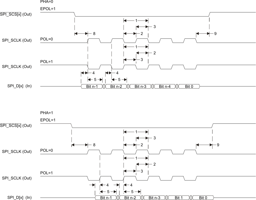 Figure 7-91 SPI Master Mode Receive Timing
Table 7-106 Timing Requirements for SPI - Slave Mode
(see Figure 7-92 and Figure 7-93)| NO. | OPP100/120/166 | UNIT | |||
|---|---|---|---|---|---|
| MIN | MAX | ||||
| 1 | tc(SPICLK) | Cycle time, SPI_CLK(1)(2) | 62.5(3) | ns | |
| 2 | tw(SPICLKL) | Pulse duration, SPI_CLK low(1) | 0.5*P - 3(4) | ns | |
| 3 | tw(SPICLKH) | Pulse duration, SPI_CLK high(1) | 0.5*P - 3(4) | ns | |
| 4 | tsu(MOSI-SPICLK) | Setup time, SPI_D[x] valid before SPI_CLK active edge(1) | 12.92 | ns | |
| 5 | th(SPICLK-MOSI) | Hold time, SPI_D[x] valid after SPI_CLK active edge(1) | 12.92 | ns | |
| 6 | td(SPICLK-MISO) | Delay time, SPI_CLK active edge to SPI_D[x] transition(1) | -4.00 | 17.1 | ns |
| 7 | td(SCS-MISO) | Delay time, SPI_SCS[x] active edge to SPI_D[x] transition(5) | 17.1 | ns | |
| 8 | tsu(SCS-SPICLK) | Setup time, SPI_SCS[x] valid before SPI_CLK first edge(1) | 12.92 | ns | |
| 9 | th(SPICLK-SCS) | Hold time, SPI_SCS[x] valid after SPI_CLK last edge(1) | 12.92 | ns | |
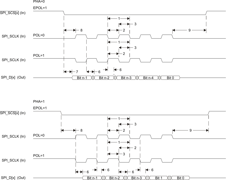 Figure 7-92 SPI Slave Mode Transmit Timing
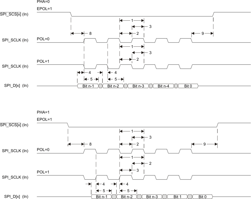 Figure 7-93 SPI Slave Mode Receive Timing
7.20 Timers
The device has eight 32-bit general-purpose (GP) timers (TIMER8 - TIMER1) that have the following features:
- TIMER8, TIMER1 are for software use and do not have an external connection
- Dedicated input trigger for capture mode and dedicated output trigger/pulse width modulation (PWM) signal
- Interrupts generated on overflow, compare, and capture
- Free-running 32-bit upward counter
- Supported modes:
- Compare and capture modes
- Auto-reload mode
- Start-stop mode
- TIMER[8:1] functional clock is sourced from either the DEVOSC, AUXOSC, AUD_CLK2/1/0, TCLKIN, or SYSCLK18 27 MHz as selected by the timer clock multiplexers.
- On-the-fly read/write register (while counting)
- Generates interrupts to the ARM and Media Controller.
The device has one system watchdog timer that have the following features:
- Free-running 32-bit upward counter
- On-the-fly read/write register (while counting)
- Reset upon occurrence of a timer overflow condition
- The system watchdog timer has two possible clock sources:
- RCOSC32K oscillator
- RTCDIVIDER
The watchdog timer is used to provide a recovery mechanism for the device in the event of a fault condition, such as a nonexiting code loop.
For more detailed information on the GP and Watchdog Timers, see the Timers and Watchdog Timer chapters of the AM387x Sitara™ ARM Processors Technical Reference Manual (Literature Number: SPRUGZ7).
7.20.1 Timer Peripheral Register Descriptions
7.20.2 Timer Electrical/Data Timing
Table 7-107 Timing Requirements for Timer
(see Figure 7-94)| NO. | OPP100/120/166 | UNIT | |||
|---|---|---|---|---|---|
| MIN | MAX | ||||
| 1 | tw(EVTIH) | Pulse duration, high | 4P(1) | ns | |
| 2 | tw(EVTIL) | Pulse duration, low | 4P(1) | ns | |
Table 7-108 Switching Characteristics Over Recommended Operating Conditions for Timer
(see Figure 7-94)| NO. | PARAMETER | OPP100/120/166 | UNIT | ||
|---|---|---|---|---|---|
| MIN | MAX | ||||
| 3 | tw(EVTOH) | Pulse duration, high | 4P-3(1) | ns | |
| 4 | tw(EVTOL) | Pulse duration, low | 4P-3(1) | ns | |
 Figure 7-94 Timer Timing
7.21 Universal Asynchronous Receiver/Transmitter (UART)
The UART performs serial-to-parallel conversions on data received from a peripheral device and parallel-to-serial conversion on data received from the CPU. The device provides up to six UART peripheral interfaces, depending on the selected pin multiplexing.
Each UART has the following features:
- Selectable UART/IrDA (SIR/MIR)/CIR modes
- Dual 64-entry FIFOs for received and transmitted data payload
- Programmable and selectable transmit and receive FIFO trigger levels for DMA and interrupt generation
- Baud-rate generation based upon programmable divisors N (N=1…16384)
- Two DMA requests and one interrupt request to the system
- Can connect to any RS-232 compliant device.
UART functions include:
- Baud-rate up to 3.6 Mbit/s on UART0, UART1, and UART2
- Baud-rate up to 12 Mbit/s on UART3, UART4, and UART5
- Programmable serial interfaces characteristics
- 5, 6, 7, or 8-bit characters
- Even, odd, or no parity-bit generation and detection
- 1, 1.5, or 2 stop-bit generation
- Flow control: hardware (RTS/CTS) or software (XON/XOFF)
- Additional modem control functions (UART0_DTR, UART0_DSR, UART0_DCD, and UART0_RIN) for UART0 only; UART1, UART2, UART3, UART4, and UART5 do not support full-flow control signaling.
IR-IrDA functions include:
- Support of IrDA 1.4 slow infrared (SIR, baud-rate up to 115.2 Kbits/s), medium infrared (MIR, baud-rate up to 1.152 Mbits/s) and fast infrared (FIR baud-rate up to 4.0 Mbits/s) communications
- Supports framing error, cyclic redundancy check (CRC) error, illegal symbol (FIR), and abort pattern (SIR, MIR) detection
- 8-entry status FIFO (with selectable trigger levels) available to monitor frame length and frame errors.
IR-CIR functions include:
- Consumer infrared (CIR) remote control mode with programmable data encoding
- Free data format (supports any remote control private standards)
- Selectable bit rate and configurable carrier frequency.
For more detailed information on the UART peripheral, see the UART/IrDA/CIR Module chapter of the AM387x Sitara™ ARM Processors Technical Reference Manual (Literature Number: SPRUGZ7).
7.21.1 UART Peripheral Register Descriptions
7.21.2 UART Electrical/Data Timing
Table 7-109 Timing Requirements for UART
(see Figure 7-95)| NO. | OPP100/120/166 | UNIT | |||
|---|---|---|---|---|---|
| MIN | MAX | ||||
| 4 | tw(RX) | Pulse width, receive data bit, 15/30/100pF high or low | 0.96U(1) | 1.05U(1) | ns |
| 5 | tw(CTS) | Pulse width, receive start bit, 15/30/100pF high or low | 0.96U(1) | 1.05U(1) | ns |
| td(RTS-TX) | Delay time, transmit start bit to transmit data | P(2) | ns | ||
| td(CTS-TX) | Delay time, receive start bit to transmit data | P(2) | ns | ||
Table 7-110 Switching Characteristics Over Recommended Operating Conditions for UART
(see Figure 7-95)| NO. | PARAMETER | OPP100/120/166 | UNIT | |||
|---|---|---|---|---|---|---|
| MIN | MAX | |||||
| f(baud) | Maximum programmable baud rate | 15 pF (UART0/1/2) | 5 | MHz | ||
| 15 pF (UART3/4/5) | 12 | |||||
| 30 pF | 0.23 | |||||
| 100 pF | 0.115 | |||||
| 2 | tw(TX) | Pulse width, transmit data bit, 15/30/100 pF high or low | U - 2(1) | U + 2(1) | ns | |
| 3 | tw(RTS) | Pulse width, transmit start bit, 15/30/100 pF high or low | U - 2(1) | U + 2(1) | ns | |
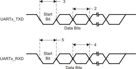 Figure 7-95 UART Timing
7.22 Universal Serial Bus (USB2.0)
The device includes two USB2.0 modules which support the Universal Serial Bus Specification Revision 2.0. The following are some of the major USB features that are supported:
- USB 2.0 peripheral at high speed (HS: 480 Mbps) and full speed (FS: 12 Mbps)
- USB 2.0 host at HS, FS, and low speed (LS: 1.5 Mbps)
- Each endpoint (other than endpoint 0, control only) can support all transfer modes (control, bulk, interrupt, and isochronous)
- Supports high-bandwidth ISO mode
- Supports 16 Transmit (TX) and 16 Receive (RX) endpoints including endpoint 0
- FIFO RAM
- 32K endpoint
- Programmable size
- Includes two integrated PHYs
- RNDIS-like mode for terminating RNDIS-type protocols without using short-packet termination for support of MSC applications.
- USB OTG extensions — session request protocol (SRP) and host negotiation protocol (HNP)
The USB2.0 peripherals do not support the following features:
- On-chip charge pump (VBUS Power must be generated external to the device.)
- RNDIS mode acceleration for USB sizes that are not multiples of 64 bytes
- Endpoint max USB packet sizes that do not conform to the USB 2.0 spec (for FS/LS: 8, 16, 32, 64, – and 1023 are defined; for HS: 64, 128, 512, and 1024 are defined
For more detailed information on the USB2.0 peripheral, see the Universal Serial Bus (USB) chapter of the AM387x Sitara™ ARM Pocessors Technical Reference Manual (Literature Number: SPRUGZ7).
7.22.1 USB2.0 Peripheral Register Descriptions
Table 7-111 USB2.0 Submodules
| SUBMODULE ADDRESS OFFSET | SUBMODULE NAME |
|---|---|
| 0x0000 | USBSS registers |
| 0x1000 | USB0 controller registers |
| 0x1800 | USB1 controller registers |
| 0x2000 | CPPI DMA controller registers |
| 0x3000 | CPPI DMA scheduler registers |
| 0x4000 | CPPI DMA Queue Manager registers |
Table 7-112 USB Subsystem (USBSS) Registers(1)
| HEX ADDRESS | ACRONYM | REGISTER NAME |
|---|---|---|
| 0x4740 0000 | REVREG | USBSS REVISION |
| 0x4740 0004 - 0x4740 000C | - | Reserved |
| 0x4740 0010 | SYSCONFIG | USBSS SYSCONFIG |
| 0x4740 0014 - 0x4740 001C | - | Reserved |
| 0x4740 0020 | EOI | USBSS IRQ_EOI |
| 0x4740 0024 | IRQSTATRAW | USBSS IRQ_STATUS_RAW |
| 0x4740 0028 | IRQSTAT | USBSS IRQ_STATUS |
| 0x4740 002C | IRQENABLER | USBSS IRQ_ENABLE_SET |
| 0x4740 0030 | IRQCLEARR | USBSS IRQ_ENABLE_CLR |
| 0x4740 0034 - 0x4740 00FC | - | Reserved |
| 0x4740 0100 | IRQDMATHOLDTX00 | USBSS IRQ_DMA_THRESHOLD_TX0_0 |
| 0x4740 0104 | IRQDMATHOLDTX01 | USBSS IRQ_DMA_THRESHOLD_TX0_1 |
| 0x4740 0108 | IRQDMATHOLDTX02 | USBSS IRQ_DMA_THRESHOLD_TX0_2 |
| 0x4740 010C | IRQDMATHOLDTX03 | USBSS IRQ_DMA_THRESHOLD_TX0_3 |
| 0x4740 0110 | IRQDMATHOLDRX00 | USBSS IRQ_DMA_THRESHOLD_RX0_0 |
| 0x4740 0114 | IRQDMATHOLDRX01 | USBSS IRQ_DMA_THRESHOLD_RX0_1 |
| 0x4740 0118 | IRQDMATHOLDRX02 | USBSS IRQ_DMA_THRESHOLD_RX0_2 |
| 0x4740 011C | IRQDMATHOLDRX03 | USBSS IRQ_DMA_THRESHOLD_RX0_3 |
| 0x4740 0120 | IRQDMATHOLDTX10 | USBSS IRQ_DMA_THRESHOLD_TX1_0 |
| 0x4740 0124 | IRQDMATHOLDTX11 | USBSS IRQ_DMA_THRESHOLD_TX1_1 |
| 0x4740 0128 | IRQDMATHOLDTX12 | USBSS IRQ_DMA_THRESHOLD_TX1_2 |
| 0x4740 012C | IRQDMATHOLDTX13 | USBSS IRQ_DMA_THRESHOLD_TX1_3 |
| 0x4740 0130 | IRQDMATHOLDRX10 | USBSS IRQ_DMA_THRESHOLD_RX1_0 |
| 0x4740 0134 | IRQDMATHOLDRX11 | USBSS IRQ_DMA_THRESHOLD_RX1_1 |
| 0x4740 0138 | IRQDMATHOLDRX12 | USBSS IRQ_DMA_THRESHOLD_RX1_2 |
| 0x4740 013C | IRQDMATHOLDRX13 | USBSS IRQ_DMA_THRESHOLD_RX1_3 |
| 0x4740 0140 | IRQDMAENABLE0 | USBSS IRQ_DMA_ENABLE_0 |
| 0x4740 0144 | IRQDMAENABLE1 | USBSS IRQ_DMA_ENABLE_1 |
| 0x4740 0148 - 0x4740 01FC | - | Reserved |
| 0x4740 0200 | IRQFRAMETHOLDTX00 | USBSS IRQ_FRAME_THRESHOLD_TX0_0 |
| 0x4740 0204 | IRQFRAMETHOLDTX01 | USBSS IRQ_FRAME_THRESHOLD_TX0_1 |
| 0x4740 0208 | IRQFRAMETHOLDTX02 | USBSS IRQ_FRAME_THRESHOLD_TX0_2 |
| 0x4740 020C | IRQFRAMETHOLDTX03 | USBSS IRQ_FRAME_THRESHOLD_TX0_3 |
| 0x4740 0210 | IRQFRAMETHOLDRX00 | USBSS IRQ_FRAME_THRESHOLD_RX0_0 |
| 0x4740 0214 | IRQFRAMETHOLDRX01 | USBSS IRQ_FRAME_THRESHOLD_RX0_1 |
| 0x4740 0218 | IRQFRAMETHOLDRX02 | USBSS IRQ_FRAME_THRESHOLD_RX0_2 |
| 0x4740 021C | IRQFRAMETHOLDRX03 | USBSS IRQ_FRAME_THRESHOLD_RX0_3 |
| 0x4740 0220 | IRQFRAMETHOLDTX10 | USBSS IRQ_FRAME_THRESHOLD_TX1_0 |
| 0x4740 0224 | IRQFRAMETHOLDTX11 | USBSS IRQ_FRAME_THRESHOLD_TX1_1 |
| 0x4740 0228 | IRQFRAMETHOLDTX12 | USBSS IRQ_FRAME_THRESHOLD_TX1_2 |
| 0x4740 022C | IRQFRAMETHOLDTX13 | USBSS IRQ_FRAME_THRESHOLD_TX1_3 |
| 0x4740 0230 | IRQFRAMETHOLDRX10 | USBSS IRQ_FRAME_THRESHOLD_RX1_0 |
| 0x4740 0234 | IRQFRAMETHOLDRX11 | USBSS IRQ_FRAME_THRESHOLD_RX1_1 |
| 0x4740 0238 | IRQFRAMETHOLDRX12 | USBSS IRQ_FRAME_THRESHOLD_RX1_2 |
| 0x4740 023C | IRQFRAMETHOLDRX13 | USBSS IRQ_FRAME_THRESHOLD_RX1_3 |
| 0x4740 0240 | IRQFRAMEENABLE0 | USBSS IRQ_FRAME_ENABLE_0 |
| 0x4740 0244 | IRQFRAMEENABLE1 | USBSS IRQ_FRAME_ENABLE_1 |
| 0x4740 0248 - 0x4740 0FFC | - | Reserved |
Table 7-113 USB0 Controller Registers
| HEX ADDRESS | ACRONYM | REGISTER NAME |
|---|---|---|
| 0x4740 1000 | USB0REV | USB0 REVISION |
| 0x4740 1004 - 0x4740 1010 | - | Reserved |
| 0x4740 1014 | USB0CTRL | USB0 Control |
| 0x4740 1018 | USB0STAT | USB0 Status |
| 0x4740 101C | - | Reserved |
| 0x4740 1020 | USB0IRQMSTAT | USB0 IRQ_MERGED_STATUS |
| 0x4740 1024 | USB0IRQEOI | USB0 IRQ_EOI |
| 0x4740 1028 | USB0IRQSTATRAW0 | USB0 IRQ_STATUS_RAW_0 |
| 0x4740 102C | USB0IRQSTATRAW1 | USB0 IRQ_STATUS_RAW_1 |
| 0x4740 1030 | USB0IRQSTAT0 | USB0 IRQ_STATUS_0 |
| 0x4740 1034 | USB0IRQSTAT1 | USB0 IRQ_STATUS_1 |
| 0x4740 1038 | USB0IRQENABLESET0 | USB0 IRQ_ENABLE_SET_0 |
| 0x4740 103C | USB0IRQENABLESET1 | USB0 IRQ_ENABLE_SET_1 |
| 0x4740 1040 | USB0IRQENABLECLR0 | USB0 IRQ_ENABLE_CLR_0 |
| 0x4740 1044 | USB0IRQENABLECLR1 | USB0 IRQ_ENABLE_CLR_1 |
| 0x4740 1048 - 0x4740 106C | - | Reserved |
| 0x4740 1070 | USB0TXMODE | USB0 Tx Mode |
| 0x4740 1074 | USB0RXMODE | USB0 Rx Mode |
| 0x4740 1078 - 0x4740 107C | - | Reserved |
| 0x4740 1080 | USB0GENRNDISEP1 | USB0 Generic RNDIS Size EP1 |
| 0x4740 1084 | USB0GENRNDISEP2 | USB0 Generic RNDIS Size EP2 |
| 0x4740 1088 | USB0GENRNDISEP3 | USB0 Generic RNDIS Size EP3 |
| 0x4740 108C | USB0GENRNDISEP4 | USB0 Generic RNDIS Size EP4 |
| 0x4740 1090 | USB0GENRNDISEP5 | USB0 Generic RNDIS Size EP5 |
| 0x4740 1094 | USB0GENRNDISEP6 | USB0 Generic RNDIS Size EP6 |
| 0x4740 1098 | USB0GENRNDISEP7 | USB0 Generic RNDIS Size EP7 |
| 0x4740 109C | USB0GENRNDISEP8 | USB0 Generic RNDIS Size EP8 |
| 0x4740 10A0 | USB0GENRNDISEP9 | USB0 Generic RNDIS Size EP9 |
| 0x4740 10A4 | USB0GENRNDISEP10 | USB0 Generic RNDIS Size EP10 |
| 0x4740 10A8 | USB0GENRNDISEP11 | USB0 Generic RNDIS Size EP11 |
| 0x4740 10AC | USB0GENRNDISEP12 | USB0 Generic RNDIS Size EP12 |
| 0x4740 10B0 | USB0GENRNDISEP13 | USB0 Generic RNDIS Size EP13 |
| 0x4740 10B4 | USB0GENRNDISEP14 | USB0 Generic RNDIS Size EP14 |
| 0x4740 10B8 | USB0GENRNDISEP15 | USB0 Generic RNDIS Size EP15 |
| 0x4740 10BC - 0x4740 10CC | - | Reserved |
| 0x4740 10D0 | USB0AUTOREQ | USB0 Auto Req |
| 0x4740 10D4 | USB0SRPFIXTIME | USB0 SRP Fix Time |
| 0x4740 10D8 | USB0TDOWN | USB0 Teardown |
| 0x4740 10DC | - | Reserved |
| 0x4740 10E0 | USB0UTMI | USB0 PHY UTMI |
| 0x4740 10E4 | USB0UTMILB | USB0 MGC UTMI Loopback |
| 0x4740 10E8 | USB0MODE | USB0 Mode |
| 0x4740 10E8 - 0x4740 13FF | - | Reserved |
| 0x4740 1400 - 0x4740 1468 | - | USB0 Mentor Core Registers/FIFOs |
| 0x4740 146C | USB0_HWVERS | USB0 Mentor Core Hardware Version Register |
| 0x4740 1470 - 0x4740 159C | - | USB0 Mentor Core Registers/FIFOs |
| 0x4740 15A0 - 0x4740 17FC | - | Reserved |
Table 7-114 USB1 Controller Registers
| HEX ADDRESS | ACRONYM | REGISTER NAME |
|---|---|---|
| 0x4740 1800 | USB1REV | USB1 Revision |
| 0x4740 1804 - 0x4740 1810 | - | Reserved |
| 0x4740 1814 | USB1CTRL | USB1 Control |
| 0x4740 1818 | USB1STAT | USB1 Status |
| 0x4740 181C | - | Reserved |
| 0x4740 1820 | USB1IRQMSTAT | USB1 IRQ_MERGED_STATUS |
| 0x4740 1824 | USB1IRQEOI | USB1 IRQ_EOI |
| 0x4740 1828 | USB1IRQSTATRAW0 | USB1 IRQ_STATUS_RAW_0 |
| 0x4740 182C | USB1IRQSTATRAW1 | USB1 IRQ_STATUS_RAW_1 |
| 0x4740 1830 | USB1IRQSTAT0 | USB1 IRQ_STATUS_0 |
| 0x4740 1834 | USB1IRQSTAT1 | USB1 IRQ_STATUS_1 |
| 0x4740 1838 | USB1IRQENABLESET0 | USB1 IRQ_ENABLE_SET_0 |
| 0x4740 183C | USB1IRQENABLESET1 | USB1 IRQ_ENABLE_SET_1 |
| 0x4740 1840 | USB1IRQENABLECLR0 | USB1 IRQ_ENABLE_CLR_0 |
| 0x4740 1844 | USB1IRQENABLECLR1 | USB1 IRQ_ENABLE_CLR_1 |
| 0x4740 1848 - 0x4740 186C | - | Reserved |
| 0x4740 1870 | USB1TXMODE | USB1 Tx Mode |
| 0x4740 1874 | USB1RXMODE | USB1 Rx Mode |
| 0x4740 1878 - 0x4740 187C | - | Reserved |
| 0x4740 1880 | USB1GENRNDISEP1 | USB1 Generic RNDIS Size EP1 |
| 0x4740 1884 | USB1GENRNDISEP2 | USB1 Generic RNDIS Size EP2 |
| 0x4740 1888 | USB1GENRNDISEP3 | USB1 Generic RNDIS Size EP3 |
| 0x4740 188C | USB1GENRNDISEP4 | USB1 Generic RNDIS Size EP4 |
| 0x4740 1890 | USB1GENRNDISEP5 | USB1 Generic RNDIS Size EP5 |
| 0x4740 1894 | USB1GENRNDISEP6 | USB1 Generic RNDIS Size EP6 |
| 0x4740 1898 | USB1GENRNDISEP7 | USB1 Generic RNDIS Size EP7 |
| 0x4740 189C | USB1GENRNDISEP8 | USB1 Generic RNDIS Size EP8 |
| 0x4740 18A0 | USB1GENRNDISEP9 | USB1 Generic RNDIS Size EP9 |
| 0x4740 18A4 | USB1GENRNDISEP10 | USB1 Generic RNDIS Size EP10 |
| 0x4740 18A8 | USB1GENRNDISEP11 | USB1 Generic RNDIS Size EP11 |
| 0x4740 18AC | USB1GENRNDISEP12 | USB1 Generic RNDIS Size EP12 |
| 0x4740 18B0 | USB1GENRNDISEP13 | USB1 Generic RNDIS Size EP13 |
| 0x4740 18B4 | USB1GENRNDISEP14 | USB1 Generic RNDIS Size EP14 |
| 0x4740 18B8 | USB1GENRNDISEP15 | USB1 Generic RNDIS Size EP15 |
| 0x4740 18BC - 0x4740 18CC | - | Reserved |
| 0x4740 18D0 | USB1AUTOREQ | USB1 Auto Req |
| 0x4740 18D4 | USB1SRPFIXTIME | USB1 SRP Fix Time |
| 0x4740 18D8 | USB1TDOWN | USB1 Teardown |
| 0x4740 18DC | - | Reserved |
| 0x4740 18E0 | USB1UTMI | USB1 PHY UTMI |
| 0x4740 18E4 | USB1UTMILB | USB1 MGC UTMI Loopback |
| 0x4740 18E8 | USB1MODE | USB1 Mode |
| 0x4740 18E8 - 0x4740 1BFF | - | Reserved |
| 0x4740 1C00 - 0x4740 1C68 | - | USB1 Mentor Core Registers |
| 0x4740 1C6C | USB1HWVERS | USB1 Mentor Core Hardware Version Register |
| 0x4740 1C70 - 0x4740 1D9C | - | USB1 Mentor Core Registers |
| 0x4740 1DA0 - 0x4740 1FFC | - | Reserved |
Table 7-115 CPPI DMA Controller Registers
| HEX ADDRESS | ACRONYM | REGISTER NAME |
|---|---|---|
| 0x4740 2000 | DMAREVID | Revision Register |
| 0x4740 2004 | TDFDQ | Teardown Free Descriptor Queue Control |
| 0x4740 2008 | DMAEMU | Emulation Control Register |
| 0x4740 200C | - | Reserved |
| 0x4740 2010 | DMAMEM1BA | CPPI Mem1 Base Address Register |
| 0x4740 2014 | DMAMEM1MASK | CPPI Mem1 Mask Address Register |
| 0x4740 200C - 0x4740 27FF | - | Reserved |
| 0x4740 2800 | TXGCR0 | Tx Channel 0 Global Configuration Register |
| 0x4740 2804 | - | Reserved |
| 0x4740 2808 | RXGCR0 | Rx Channel 0 Global Configuration Register |
| 0x4740 280C | RXHPCRA0 | Rx Channel 0 Host Packet Configuration Register A |
| 0x4740 2810 | RXHPCRB0 | Rx Channel 0 Host Packet Configuration Register B |
| 0x4740 2814 - 0x4740 281C | - | Reserved |
| 0x4740 2820 | TXGCR1 | Tx Channel 1 Global Configuration Register |
| 0x4740 2824 | - | Reserved |
| 0x4740 2828 | RXGCR1 | Rx Channel 1 Global Configuration Register |
| 0x4740 282C | RXHPCRA1 | Rx Channel 1 Host Packet Configuration Register A |
| 0x4740 2830 | RXHPCRB1 | Rx Channel 1 Host Packet Configuration Register B |
| 0x4740 2834 - 0x4740 283C | - | Reserved |
| 0x4740 2840 | TXGCR2 | Tx Channel 2 Global Configuration Register |
| 0x4740 2844 | - | Reserved |
| 0x4740 2848 | RXGCR2 | Rx Channel 2 Global Configuration Register |
| 0x4740 284C | RXHPCRA2 | Rx Channel 2 Host Packet Configuration Register A |
| 0x4740 2850 | RXHPCRB2 | Rx Channel 2 Host Packet Configuration Register B |
| 0x4740 2854 - 0x4740 285F | - | Reserved |
| 0x4740 2860 | TXGCR3 | Tx Channel 3 Global Configuration Register |
| 0x4740 2864 | - | Reserved |
| 0x4740 2868 | RXGCR3 | Rx Channel 3 Global Configuration Register |
| 0x4740 286C | RXHPCRA3 | Rx Channel 3 Host Packet Configuration Register A |
| 0x4740 2870 | RXHPCRB3 | Rx Channel 3 Host Packet Configuration Register B |
| 0x4740 2880 - 0x4740 2B9F | - | ... |
| 0x4740 2BA0 | TXGCR29 | Tx Channel 29 Global Configuration Register |
| 0x4740 2BA4 | - | Reserved |
| 0x4740 2BA8 | RXGCR29 | Rx Channel 29 Global Configuration Register |
| 0x4740 2BAC | RXHPCRA29 | Rx Channel 29 Host Packet Configuration Register A |
| 0x4740 2BB0 | RXHPCRB29 | Rx Channel 29 Host Packet Configuration Register B |
| 0x4740 2BB4 - 0x4740 2FFF | - | Reserved |
Table 7-116 CPPI DMA Scheduler Registers
| HEX ADDRESS | ACRONYM | REGISTER NAME |
|---|---|---|
| 0x4740 3000 | DMA_SCHED_CTRL | CPPI DMA Scheduler Control Register |
| 0x4740 3804 - 0x4740 38FF | - | Reserved |
| 0x4740 3800 | WORD0 | CPPI DMA Scheduler Table Word 0 |
| 0x4740 3804 | WORD1 | CPPI DMA Scheduler Table Word 1 |
| … | … | … |
| 0x4740 38F8 | WORD62 | CPPI DMA Scheduler Table Word 62 |
| 0x4740 38FC | WORD63 | CPPI DMA Scheduler Table Word 63 |
| 0x4740 38FF - 0x4740 3FFF | - | Reserved |
Table 7-117 CPPI DMA Queue Manager Registers
| HEX ADDRESS | ACRONYM | REGISTER NAME |
|---|---|---|
| 0x4740 4000 | QMGRREVID | Queue Manager Revision |
| 0x4740 4004 | - | Reserved |
| 0x4740 4008 | DIVERSION | Queue Manager Queue Diversion |
| 0x4740 400C - 0x4740 401F | - | Reserved |
| 0x4740 4020 | FDBSC0 | Queue Manager Free Descriptor/Buffer Starvation Count 0 |
| 0x4740 4024 | FDBSC1 | Queue Manager Free Descriptor/Buffer Starvation Count 1 |
| 0x4740 4028 | FDBSC2 | Queue Manager Free Descriptor/Buffer Starvation Count 2 |
| 0x4740 402C | FDBSC3 | Queue Manager Free Descriptor/Buffer Starvation Count 3 |
| 0x4740 4030 | FDBSC4 | Queue Manager Free Descriptor/Buffer Starvation Count 4 |
| 0x4740 4034 | FDBSC5 | Queue Manager Free Descriptor/Buffer Starvation Count 5 |
| 0x4740 4038 | FDBSC6 | Queue Manager Free Descriptor/Buffer Starvation Count 6 |
| 0x4740 403C | FDBSC7 | Queue Manager Free Descriptor/Buffer Starvation Count 7 |
| 0x4740 4030 - 0x4740 407C | - | Reserved |
| 0x4740 4080 | LRAM0BASE | Queue Manager Linking RAM Region 0 Base Address |
| 0x4740 4084 | LRAM0SIZE | Queue Manager Linking RAM Region 0 Size |
| 0x4740 4088 | LRAM1BASE | Queue Manager Linking RAM Region 1 Base Address |
| 0x4740 408C | - | Reserved |
| 0x4740 4090 | PEND0 | Queue Manager Queue Pending 0 |
| 0x4740 4094 | PEND1 | Queue Manager Queue Pending 1 |
| 0x4740 4098 | PEND2 | Queue Manager Queue Pending 2 |
| 0x4740 409C | PEND3 | Queue Manager Queue Pending 3 |
| 0x4740 40A0 | PEND4 | Queue Manager Queue Pending 4 |
| 0x4740 40A4 - 0x4740 4FFF | - | Reserved |
| 0x4740 5000 + 16xR | QMEMRBASE0 | Memory Region 0 Base Address (R ranges from 0 to 15) |
| 0x4740 5000 + 16xR + 4 | QMEMRCTRL0 | Memory Region 0 Control 0 (R ranges from 0 to 15) |
| 0x4740 5000 + 16xR + 8 | - | Reserved |
| 0x4740 5000 + 16xR + C | - | Reserved |
| 0x4740 5010 – 0x4740 50EF | - | ... |
| 0x4740 5000 + 16xR | QMEMRBASE15 | Memory Region 15 Base Address (R ranges from 0 to 15) |
| 0x4740 5000 + 16xR + 4 | QMEMRCTRL15 | Memory Region 15 Control (R ranges from 0 to 15) |
| 0x4740 5000 + 16xR + 8 | - | Reserved |
| 0x4740 5000 + 16xR + C | - | Reserved |
| 0x4740 5080 - 0x4740 5FFF | - | Reserved |
| 0x4740 6000 + 16xN | - | Reserved |
| 0x4740 6000 + 16xN + 4 | - | Reserved |
| 0x4740 6000 + 16xN + 8 | - | Reserved |
| 0x4740 6000 + 16xN + C | CTRLD0 | Queue N Register D (N ranges from 0 to 155) |
| 0x4740 6010 – 0x4740 69AF | - | ... |
| 0x4740 6000 + 16xN | - | Reserved |
| 0x4740 6000 + 16xN + 4 | - | Reserved |
| 0x4740 6000 + 16xN + 8 | - | Reserved |
| 0x4740 6000 + 16xN + C | CTRLD155 | Queue N Register D (N ranges from 0 to 155) |
| 0x4740 69B0 - 0x4740 6FFF | - | Reserved |
| 0x4740 7000 + 16xN | QSTATA0 | Queue N Status A (N ranges from 0 to 155) |
| 0x4740 7000 + 16xN + 4 | QSTATB0 | Queue N Status B (N ranges from 0 to 155) |
| 0x4740 7000 + 16xN + 8 | QSTATC0 | Queue N Status C (N ranges from 0 to 155) |
| 0x4740 7000 + 16xN + C | - | Reserved |
| 0x4740 7010 – 0x4740 79AF | - | ... |
| 0x4740 7000 + 16xN | QSTATA155 | Queue N Status A (N ranges from 0 to 155) |
| 0x4740 7000 + 16xN + 4 | QSTATB155 | Queue N Status B (N ranges from 0 to 155) |
| 0x4740 7000 + 16xN + 8 | QSTATC155 | Queue N Status C (N ranges from 0 to 155) |
| 0x4740 7000 + 16xN + C | - | Reserved |
| 0x4740 79B0 - 0x4740 7FFF | - | Reserved |
7.22.2 USB2.0 Electrical Data/Timing
Table 7-118 Switching Characteristics Over Recommended Operating Conditions for USB2.0
(see Figure 7-96)| NO. | PARAMETER | OPP100/120/166 | UNIT | ||||||
|---|---|---|---|---|---|---|---|---|---|
| LOW SPEED 1.5 Mbps |
FULL SPEED 12 Mbps |
HIGH SPEED 480 Mbps |
|||||||
| MIN | MAX | MIN | MAX | MIN | MAX | ||||
| 1 | tr(D) | Rise time, USBx_DP and USBx_DM signals(1) | 75 | 300 | 4 | 20 | 0.5 | ns | |
| 2 | tf(D) | Fall time, USBx_DP and USBx_DM signals(1) | 75 | 300 | 4 | 20 | 0.5 | ns | |
| 3 | trfM | Rise/Fall time, matching(2) | 80 | 125 | 90 | 111 | – | – | % |
| 4 | VCRS | Output signal cross-over voltage(1) | 1.3 | 2 | 1.3 | 2 | – | – | V |
| 5 | tjr(source)NT | Source (Host) Driver jitter, next transition | 2 | 2 | (4) | ns | |||
| tjr(FUNC)NT | Function Driver jitter, next transition | 25 | 2 | (4) | ns | ||||
| 6 | tjr(source)PT | Source (Host) Driver jitter, paired transition(3) | 1 | 1 | (4) | ns | |||
| tjr(FUNC)PT | Function Driver jitter, paired transition | 10 | 1 | (4) | ns | ||||
| 7 | tw(EOPT) | Pulse duration, EOP transmitter | 1250 | 1500 | 160 | 175 | – | – | ns |
| 8 | tw(EOPR) | Pulse duration, EOP receiver(5) | 670 | 82 | – | ns | |||
| 9 | t(DRATE) | Data Rate | 1.5 | 12 | 480 | Mbps | |||
| 10 | ZDRV | Driver Output Resistance | – | – | 28 | 49.5 | 40.5 | 49.5 | Ω |
| 11 | ZINP | Receiver Input Impedance(6) | 300 | 300 | – | – | – | kΩ | |
 Figure 7-96 USB2.0 Integrated Transceiver Interface Timing
For more detailed information on USB2.0 board design, routing, and layout guidelines, see the USB 2.0 Board Design and Layout Guidelines Application Report (Literature Number: SPRAAR7).