SBAS734C March 2017 – Janaury 2020 AMC1306E05 , AMC1306E25 , AMC1306M05 , AMC1306M25
PRODUCTION DATA.
- 1 Features
- 2 Applications
- 3 Description
- 4 Revision History
- 5 Device Comparison Table
- 6 Pin Configuration and Functions
-
7 Specifications
- 7.1 Absolute Maximum Ratings
- 7.2 ESD Ratings
- 7.3 Recommended Operating Conditions
- 7.4 Thermal Information
- 7.5 Power Ratings
- 7.6 Insulation Specifications
- 7.7 Safety-Related Certifications
- 7.8 Safety Limiting Values
- 7.9 Electrical Characteristics: AMC1306x05
- 7.10 Electrical Characteristics: AMC1306x25
- 7.11 Switching Characteristics
- 7.12 Insulation Characteristics Curves
- 7.13 Typical Characteristics
- 8 Detailed Description
- 9 Application and Implementation
- 10Power Supply Recommendations
- 11Layout
- 12Device and Documentation Support
- 13Mechanical, Packaging, and Orderable Information
Package Options
Refer to the PDF data sheet for device specific package drawings
Mechanical Data (Package|Pins)
- DWV|8
Thermal pad, mechanical data (Package|Pins)
Orderable Information
8.4.1 Fail-Safe Output
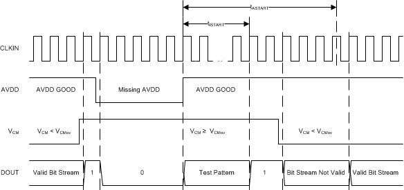
In the case of a missing high-side supply voltage AVDD, the output of a ΔΣ modulator is not defined and can cause a system malfunction. In systems with high safety requirements, this behavior is not acceptable. Therefore, the AMC1306 implements a fail-safe output function that ensures that the output DOUT of the device offers a steady-state bitstream of logic 0's in case of a missing AVDD, as shown in Figure 53.
Additionally, if the common-mode voltage of the input reaches or exceeds the specified common-mode overvoltage detection level VCMov as defined in the Electrical Characteristics table, the AMC1306 offers a steady-state bitstream of logic 1's at the output DOUT, as also shown in Figure 53.
 Figure 53. Fail-Safe Output of the AMC1306