SBAS734C March 2017 – Janaury 2020 AMC1306E05 , AMC1306E25 , AMC1306M05 , AMC1306M25
PRODUCTION DATA.
- 1 Features
- 2 Applications
- 3 Description
- 4 Revision History
- 5 Device Comparison Table
- 6 Pin Configuration and Functions
-
7 Specifications
- 7.1 Absolute Maximum Ratings
- 7.2 ESD Ratings
- 7.3 Recommended Operating Conditions
- 7.4 Thermal Information
- 7.5 Power Ratings
- 7.6 Insulation Specifications
- 7.7 Safety-Related Certifications
- 7.8 Safety Limiting Values
- 7.9 Electrical Characteristics: AMC1306x05
- 7.10 Electrical Characteristics: AMC1306x25
- 7.11 Switching Characteristics
- 7.12 Insulation Characteristics Curves
- 7.13 Typical Characteristics
- 8 Detailed Description
- 9 Application and Implementation
- 10Power Supply Recommendations
- 11Layout
- 12Device and Documentation Support
- 13Mechanical, Packaging, and Orderable Information
Package Options
Refer to the PDF data sheet for device specific package drawings
Mechanical Data (Package|Pins)
- DWV|8
Thermal pad, mechanical data (Package|Pins)
Orderable Information
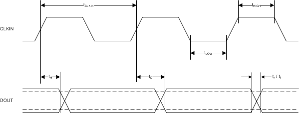
7.11 Switching Characteristics
over operating ambient temperature range (unless otherwise noted)| PARAMETER | TEST CONDITIONS | MIN | TYP | MAX | UNIT | |
|---|---|---|---|---|---|---|
| fCLKIN | CLKIN clock frequency | 4.5 V ≤ AVDD ≤ 5.5 V | 5 | 21 | MHz | |
| 3.0 V ≤ AVDD ≤ 5.5 V | 5 | 20 | ||||
| tCLKIN | CLKIN clock period | 4.5 V ≤ AVDD ≤ 5.5 V | 47.6 | 200 | ns | |
| 3.0 V ≤ AVDD ≤ 5.5 V | 50 | 200 | ||||
| tHIGH | CLKIN clock high time | 20 | 25 | 120 | ns | |
| tLOW | CLKIN clock low time | 20 | 25 | 120 | ns | |
| tH | DOUT hold time after rising edge
of CLKIN |
AMC1306Mx(1),
CLOAD = 15 pF |
3.5 | ns | ||
| tD | Rising edge of CLKIN to DOUT valid delay | AMC1306Mx(1), CLOAD = 15 pF | 15 | ns | ||
| tr | DOUT rise time | 10% to 90%, 2.7 V ≤ DVDD ≤ 3.6 V,
CLOAD = 15 pF |
0.8 | 3.5 | ns | |
| 10% to 90%, 4.5 V ≤ DVDD ≤ 5.5 V,
CLOAD = 15 pF |
1.8 | 3.9 | ||||
| tf | DOUT fall time | 90% to 10%, 2.7 V ≤ DVDD ≤ 3.6 V,
CLOAD = 15 pF |
0.8 | 3.5 | ns | |
| 90% to 10%, 4.5 V ≤ DVDD ≤ 5.5 V,
CLOAD = 15 pF |
1.8 | 3.9 | ||||
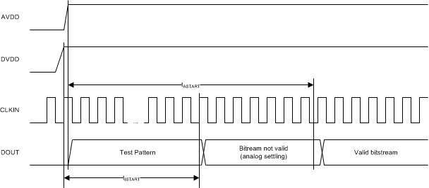
| tISTART | Interface startup time | DVDD at 2.7 V (min) to DOUT valid with AVDD ≥ 3.0 V | 32 | 32 | CLKIN cycles | |
| tASTART | Analog startup time | AVDD step to 3.0 V with DVDD ≥ 2.7 V, 0.1% settling | 0.5 | ms | ||
(1) The output of the Manchester encoded versions of the AMC1306Ex can change with every edge of CLKIN with a typical delay of 6 ns; see the Manchester Coding Feature section for additional details.
 Figure 1. Digital Interface Timing
  Figure 2. Device Startup Timing