SBAS994B September 2023 – September 2023 AMC131M03
PRODUCTION DATA
- 1
- 1 Features
- 2 Applications
- 3 Description
- 4 Revision History
- 5 Pin Configuration and Functions
-
6 Specifications
- 6.1 Absolute Maximum Ratings
- 6.2 ESD Ratings
- 6.3 Recommended Operating Conditions
- 6.4 Thermal Information
- 6.5 Insulation Specifications
- 6.6 Safety-Related Certifications
- 6.7 Safety Limiting Values
- 6.8 Electrical Characteristics
- 6.9 Timing Requirements
- 6.10 Switching Characteristics
- 6.11 Timing Diagrams
- 6.12 Typical Characteristics
- 7 Parameter Measurement Information
-
8 Detailed Description
- 8.1 Overview
- 8.2 Functional Block Diagram
- 8.3
Feature Description
- 8.3.1 Isolated DC/DC Converter
- 8.3.2 High-Side Current Drive Capability
- 8.3.3 Isolation Channel Signal Transmission
- 8.3.4 Input ESD Protection Circuitry
- 8.3.5 Input Multiplexer
- 8.3.6 Programmable Gain Amplifier (PGA)
- 8.3.7 Voltage Reference
- 8.3.8 Internal Test Signals
- 8.3.9 Clocking and Power Modes
- 8.3.10 ΔΣ Modulator
- 8.3.11 Digital Filter
- 8.3.12 Channel Phase Calibration
- 8.3.13 Calibration Registers
- 8.3.14 Register Map CRC
- 8.3.15 Temperature Sensor
- 8.3.16 General-Purpose Digital Output (GPO)
- 8.4 Device Functional Modes
- 8.5
Programming
- 8.5.1
Serial Interface
- 8.5.1.1 Chip Select (CS)
- 8.5.1.2 Serial Data Clock (SCLK)
- 8.5.1.3 Serial Data Input (DIN)
- 8.5.1.4 Serial Data Output (DOUT)
- 8.5.1.5 Data Ready (DRDY)
- 8.5.1.6 Conversion Synchronization or System Reset (SYNC/RESET)
- 8.5.1.7 SPI Communication Frames
- 8.5.1.8 SPI Communication Words
- 8.5.1.9 Short SPI Frames
- 8.5.1.10 Communication Cyclic Redundancy Check (CRC)
- 8.5.1.11 SPI Timeout
- 8.5.2 ADC Conversion Data
- 8.5.3 Commands
- 8.5.4 ADC Output Buffer and FIFO Buffer
- 8.5.5 Collecting Data for the First Time or After a Pause in Data Collection
- 8.5.1
Serial Interface
- 8.6 AMC131M03 Registers
- 9 Application and Implementation
- 10Device and Documentation Support
- 11Mechanical, Packaging, and Orderable Information
Package Options
Mechanical Data (Package|Pins)
- DFM|20
Thermal pad, mechanical data (Package|Pins)
Orderable Information
9.2.2.1 Voltage Measurement
The nominal mains voltage ranges from 100 V to 240 V, so this voltage must be scaled down to be sensed by an ADC. Figure 9-5 shows the analog front-end used for this voltage scaling at the ADC channel 1.
The analog front-end for voltage measurement consists of a voltage divider network (RHI and RLO), and an RC low-pass filter (RFILT and CFILT). Additional protection components (such as spike protection varistors) are usually placed as well, but are not shown in this circuit for simplicity.
Equation 17 shows how to calculate the range of differential voltages fed to the voltage ADC channel for a given mains voltage and the selected voltage divider resistor values.
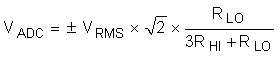
RHI is 300 kΩ and RLO is 750 Ω in a typical design. For a mains voltage of 240 V (as measured between the line and neutral), the input signal to the voltage-sensing ADC has a voltage swing of ±256 mV (182 mVRMS) based on Equation 17 and the selected resistor values. This voltage is well within the ±1.2-V input voltage range that can be sensed by the AMC131M03 for the selected PGA gain value of 1 that is used for the voltage channels. In addition, overvoltages as high as four times the main voltages (up to 1000 V) can also be measured based on the selected combination of resistor values and gain setting.
The finite input impedance of the ADC channel 1 results in a gain error and offset error from the non-ideal voltage division by RLO. The introduction of a resistor in series with the inverting input of the ADC can reduce the offset and gain errors, as explained in the Isolated Voltage-Measurement Circuit With ±250-mV Input and Differential Output application note. The value of the additional series resistor is recommended to be in the order of RLO, and the design steps are documented in the Isolated Voltage-Measurement Circuit With ±250-mV Input and Differential Output application note.