SBASA84A February 2021 – July 2021 AMC3302-Q1
PRODUCTION DATA
- 1 Features
- 2 Applications
- 3 Description
- 4 Revision History
- 5 Pin Configuration and Functions
-
6 Specifications
- 6.1 Absolute Maximum Ratings
- 6.2 ESD Ratings
- 6.3 Recommended Operating Conditions
- 6.4 Thermal Information
- 6.5 Power Ratings
- 6.6 Insulation Specifications
- 6.7 Safety-Related Certifications
- 6.8 Safety Limiting Values
- 6.9 Electrical Characteristics
- 6.10 Switching Characteristics
- 6.11 Timing Diagram
- 6.12 Insulation Characteristics Curves
- 6.13 Typical Characteristics
- 7 Detailed Description
- 8 Application and Implementation
- 9 Power Supply Recommendations
- 10Layout
- 11Device and Documentation Support
- 12Mechanical, Packaging, and Orderable Information
Package Options
Mechanical Data (Package|Pins)
- DWE|16
Thermal pad, mechanical data (Package|Pins)
Orderable Information
7.3.3 Analog Output
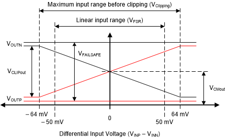
The AMC3302-Q1 offers a differential analog output comprised of the OUTP and OUTN pins. For differential input voltages (VINP – VINN) in the range from –50 mV to 50 mV, the device provides a linear response with a nominal gain of 41. For example, for a differential input voltage of 50 mV, the differential output voltage (VOUTP – VOUTN) is 2.05 V. At zero input (INP shorted to INN), both pins output the same common-mode output voltage VCMout, as specified in the Section 6.9 table. For absolute differential input voltages greater than 50 mV but less than 64 mV, the differential output voltage continues to increase in magnitude but with reduced linearity performance. The outputs saturate at a differential output voltage of VCLIPout, as shown in Figure 7-2, if the differential input voltage exceeds the VClipping value.
 Figure 7-2 Output Behavior of the AMC3302-Q1
The AMC3302-Q1 provides a failsafe output that simplifies diagnostics on system level. Figure 7-2 shows the failsafe mode, in which the AMC3302-Q1 outputs a negative differential output voltage that does not occur under normal operating conditions. The failsafe output is active in two cases:
- The low-side does not receive data from the high-side (for example, because of a loss of power on the high side)
- The high-side DC/DC output voltage (DCDC_OUT) or the high-side LDO output voltage (HLDO_OUT) drop below their respective undervoltage detection thresholds (brown-out)
Use the maximum VFAILSAFE voltage specified in the Section 6.9 table as a reference value for the failsafe detection on the system level.