SBASA35A June 2020 – October 2020 AMC3330-Q1
PRODUCTION DATA
- 1 Features
- 2 Applications
- 3 Description
- 4 Revision History
- 5 Pin Configuration and Functions
-
6 Specifications
- 6.1 Absolute Maximum Ratings
- 6.2 ESD Ratings
- 6.3 Recommended Operating Conditions
- 6.4 Thermal Information
- 6.5 Power Ratings
- 6.6 Insulation Specifications
- 6.7 Safety-Related Certifications
- 6.8 Safety Limiting Values
- 6.9 Electrical Characteristics
- 6.10 Switching Characteristics
- 6.11 Timing Diagram
- 6.12 Insulation Characteristics Curves
- 6.13 Typical Characteristics
- 7 Detailed Description
- 8 Application and Implementation
- 9 Power Supply Recommendations
- 10Layout
- 11Device and Documentation Support
- 12Mechanical, Packaging, and Orderable Information
Package Options
Mechanical Data (Package|Pins)
- DWE|16
Thermal pad, mechanical data (Package|Pins)
Orderable Information
8.2 Typical Application
Isolated amplifiers are widely used for voltage measurements in high-voltage applications that must be isolated from a low-voltage domain. Typical applications are AC line voltage measurements at the input of a power factor correction (PFC) stage of an onboard charger (OBC). Other applications are DC measurements at the output of a PFC stage or DC/DC converter, or phase voltage measurements in traction inverters. The AMC3330-Q1 integrates an isolated power supply for the high-voltage side and therefore is particularly easy to use in applications that do not have a high-side supply readily available or where a high-side supply is referenced to a different ground potential than the signal to be measured.
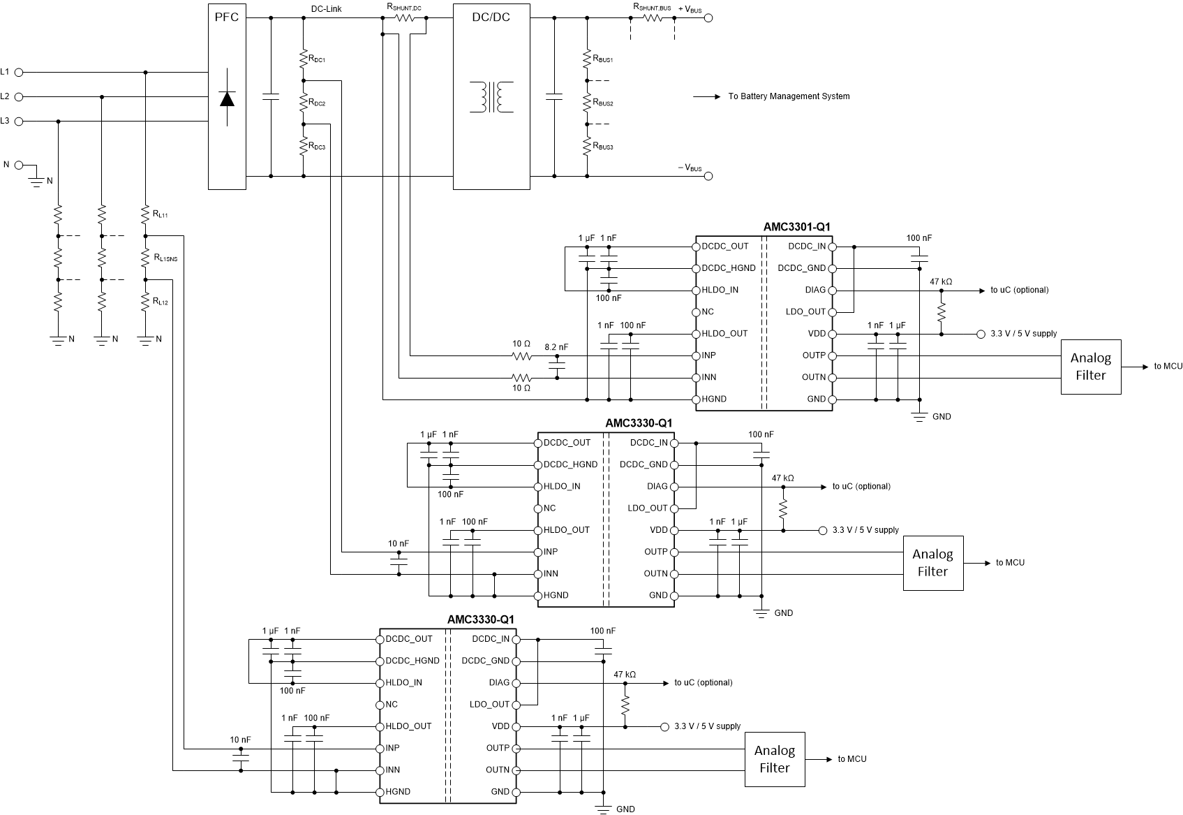
Figure 8-1 illustrates a simplified schematic of the AMC3330-Q1 in an OBC where the AC phase voltage on the grid-side must to be measured. At that location in the system, there is no supply readily available for powering the isolated amplifier. The integrated isolated power supply, together with its bipolar input voltage range, makes the AMC3330-Q1 ideally suited for AC line-voltage sensing. In this example, the output current of the PFC is sensed by the AMC3301-Q1 across a shunt resistor on the positive DC-link rail where there is also no suitable supply available for powering the isolated amplifier. The integrated power-supply of the AMC3301-Q1 eliminates that problem and enables current sensing at optimal locations for the system.
 Figure 8-1 The AMC3330-Q1 in an OBC Application