SLVSDU6D July   2017  – November 2019 ATL431LI , ATL432LI

PRODUCTION DATA.  

  1. Features
  2. Applications
  3. Description
    1.     Device Images
      1.      Simplified Schematic
  4. Revision History
  5. Device Comparison Table
  6. Pin Configuration and Functions
    1.     Pin Functions
  7. Specifications
    1. 7.1 Absolute Maximum Ratings
    2. 7.2 ESD Ratings
    3. 7.3 Thermal Information
    4. 7.4 Recommended Operating Conditions
    5. 7.5 Electrical Characteristics
  8. Typical Characteristics
  9. Parameter Measurement Information
    1. 9.1 Temperature Coefficient
    2. 9.2 Dynamic Impedance
  10. 10Detailed Description
    1. 10.1 Overview
    2. 10.2 Functional Block Diagram
    3. 10.3 Feature Description
    4. 10.4 Device Functional Modes
      1. 10.4.1 Open Loop (Comparator)
      2. 10.4.2 Closed Loop
  11. 11Applications and Implementation
    1. 11.1 Application Information
    2. 11.2 Typical Applications
      1. 11.2.1 Comparator With Integrated Reference
        1. 11.2.1.1 Design Requirements
        2. 11.2.1.2 Detailed Design Procedure
          1. 11.2.1.2.1 Basic Operation
            1. 11.2.1.2.1.1 Overdrive
          2. 11.2.1.2.2 Output Voltage and Logic Input Level
            1. 11.2.1.2.2.1 Input Resistance
        3. 11.2.1.3 Application Curve
      2. 11.2.2 Precision Constant Current Sink
        1. 11.2.2.1 Design Requirements
        2. 11.2.2.2 Detailed Design Procedure
          1. 11.2.2.2.1 Basic Operation
            1. 11.2.2.2.1.1 Output Current Range and Accuracy
          2. 11.2.2.2.2 Power Consumption
      3. 11.2.3 Shunt Regulator/Reference
        1. 11.2.3.1 Design Requirements
        2. 11.2.3.2 Detailed Design Procedure
          1. 11.2.3.2.1 Programming Output/Cathode Voltage
          2. 11.2.3.2.2 Total Accuracy
          3. 11.2.3.2.3 Stability
          4. 11.2.3.2.4 Start-Up Time
        3. 11.2.3.3 Application Curve
      4. 11.2.4 Isolated Flyback with Optocoupler
        1. 11.2.4.1 Design Requirements
          1. 11.2.4.1.1 Detailed Design Procedure
            1. 11.2.4.1.1.1 ATL431LI Biasing
            2. 11.2.4.1.1.2 Resistor Feedback Network
    3. 11.3 System Examples
  12. 12Power Supply Recommendations
  13. 13Layout
    1. 13.1 Layout Guidelines
    2. 13.2 SOT23-3 Layout Example
    3. 13.3 X2SON (DQN) Layout Example
    4. 13.4 Thermal Considerations
  14. 14Device and Documentation Support
    1. 14.1 Documentation Support
      1. 14.1.1 Device Nomenclature
      2. 14.1.2 Related Documentation
    2. 14.2 Related Links
    3. 14.3 Receiving Notification of Documentation Updates
    4. 14.4 Community Resources
    5. 14.5 Trademarks
    6. 14.6 Electrostatic Discharge Caution
    7. 14.7 Glossary
  15. 15Mechanical, Packaging, and Orderable Information

Package Options

Mechanical Data (Package|Pins)
Thermal pad, mechanical data (Package|Pins)
Orderable Information

Detailed Design Procedure

In this example a simplified design procedure will be discussed. The compensation network for the feedback network is beyond the scope of this section. Details on compensation network can be found on SLUA671.

The goal of this design is to design a low standby current feedback network to meet the Europe CoC Tier 2 and United States DoE Level VI requirements. To meet the design requirements, the system standby power needs to be below 75mW. In order to meet this, the feedback network needs to consume less than 40mW to allow margin for the power losses on the primary side controller and passive components and this can pose a challenge in systems greater than 10V.
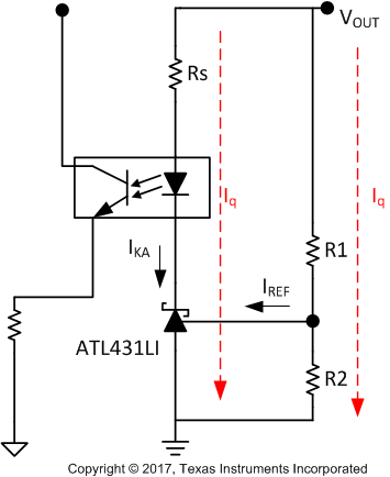
ATL431LI ATL432LI Currents.gifFigure 29. Feedback Quiescent Current