SLUS938A December   2011  – October 2014

PRODUCTION DATA.  

  1. 1Features
  2. 2Applications
  3. 3Description
  4. 4Revision History
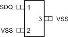
  5. 5Pin Configuration and Functions
  6. 6Specifications
    1. 6.1 Absolute Maximum Ratings
    2. 6.2 Handling Ratings
    3. 6.3 Electrical Characteristics: DC
    4. 6.4 Switching Characteristcs: AC
  7. 7Detailed Description
    1. 7.1 Overview
    2. 7.2 Functional Block Diagram
    3. 7.3 Feature Description
      1. 7.3.1 EPROM
      2. 7.3.2 EPROM Status Memory
      3. 7.3.3 Error Checking
    4. 7.4 Device Functional Modes
      1. 7.4.1  Customizing the bq2026
      2. 7.4.2  Bus Termination
      3. 7.4.3  Serial Communication
      4. 7.4.4  Initialization
      5. 7.4.5  ROM Commands
        1. 7.4.5.1 Read ROM
        2. 7.4.5.2 Match ROM
        3. 7.4.5.3 Skip ROM
      6. 7.4.6  Memory and Status Function Commands
      7. 7.4.7  Read Memory and Field CRC
      8. 7.4.8  Read Status
      9. 7.4.9  Write Memory
      10. 7.4.10 Write Status
      11. 7.4.11 SDQ Signaling
      12. 7.4.12 Reset and Presence Pulse
      13. 7.4.13 Write
      14. 7.4.14 Read
      15. 7.4.15 Program Pulse
      16. 7.4.16 Idle
      17. 7.4.17 CRC Generation
  8. 8Device and Documentation Support
    1. 8.1 Trademarks
    2. 8.2 Electrostatic Discharge Caution
    3. 8.3 Glossary
  9. 9Mechanical, Packaging, and Orderable Information

Package Options

Mechanical Data (Package|Pins)
Thermal pad, mechanical data (Package|Pins)
Orderable Information

5 Pin Configuration and Functions

DBZ Package
SOT-23-3
(Top View)
po_dbz_lus938.gif
LP Package
TO-92-3
(Top View)
po_lp_lus938.gif

Pin Functions

PIN I/O DESCRIPTION
NAME DBZ LP
SDQ 1 2 I/O Data
VSS 2, 3 1 Ground
VSS 3 Can be ground or left unconnected