SLUS698F March 2006 – May 2017
PRODUCTION DATA.
- 1 Features
- 2 Applications
- 3 Description
- 4 Revision History
- 5 Pin Configuration and Functions
- 6 Specifications
-
7 Detailed Description
- 7.1 Overview
- 7.2 Functional Block Diagram
- 7.3
Feature Description
- 7.3.1 Battery Preconditioning
- 7.3.2 Battery Fast-Charge Constant Current
- 7.3.3 Charge-Current Monitor
- 7.3.4 Battery Fast-Charge Voltage Regulation
- 7.3.5 Charge Termination Detection and Recharge
- 7.3.6 Charge Status Outputs
- 7.3.7 PG Output (bq24080)
- 7.3.8 Charge-Enabled (CE) Input (bq24080)
- 7.3.9 Timer Enabled (TE) Input (bq24081)
- 7.3.10 Temperature Qualification (bq24081)
- 7.3.11 Timer Fault and Recovery
- 7.4 Device Functional Modes
- 8 Application and Implementation
- 9 Power Supply Recommendations
- 10Layout
- 11Device and Documentation Support
- 12Mechanical, Packaging, and Orderable Information
Package Options
Mechanical Data (Package|Pins)
- DRC|10
Thermal pad, mechanical data (Package|Pins)
- DRC|10
Orderable Information
6 Specifications
6.1 Absolute Maximum Ratings
over operating free-air temperature range (unless otherwise noted)(1)| MIN | MAX | UNIT | |||
|---|---|---|---|---|---|
| VI | Input voltage(2) | IN, CE, ISET, OUT, PG, STAT1, STAT2, TE, TS | –0.3 | 7 | V |
| Output sink/source current | STAT1, STAT2, PG | 15 | mA | ||
| Output current | OUT | 1.5 | A | ||
| TA | Operating free-air temperature range | –40 | 125 | °C | |
| TJ | Junction temperature range | °C | |||
| Tstg | Storage temperature | –65 | 150 | °C | |
(1) Stresses beyond those listed under Absolute Maximum Ratings may cause permanent damage to the device. These are stress ratings only, which do not imply functional operation of the device at these or any other conditions beyond those indicated under Recommended Operating Conditions. Exposure to absolute-maximum-rated conditions for extended periods may affect device reliability.
(2) All voltages are with respect to VSS.
6.2 ESD Ratings
| VALUE | UNIT | |||
|---|---|---|---|---|
| V(ESD) | Electrostatic discharge | Human-body model (HBM), per ANSI/ESDA/JEDEC JS-001(1) | ±2000 | V |
| Charged-device model (CDM), per JEDEC specification JESD22-C101(2) | ±500 | |||
(1) JEDEC document JEP155 states that 500-V HBM allows safe manufacturing with a standard ESD control process.
(2) JEDEC document JEP157 states that 250-V CDM allows safe manufacturing with a standard ESD control process.
6.3 Recommended Operating Conditions
over operating free-air temperature range (unless otherwise noted)| MIN | MAX | UNIT | ||
|---|---|---|---|---|
| VCC | Supply voltage | 4.5 | 6.5 | V |
| TJ | Operating junction temperature range | 0 | 125 | °C |
6.4 Thermal Information
| THERMAL METRIC(1) | bq2408x | UNIT | |
|---|---|---|---|
| DRC (VSON) | |||
| 10 PINS | |||
| RθJA | Junction-to-ambient thermal resistance | 49.4 | °C/W |
| RθJC(top) | Junction-to-case (top) thermal resistance | 69.8 | °C/W |
| RθJB | Junction-to-board thermal resistance | 23.9 | °C/W |
| ψJT | Junction-to-top characterization parameter | 2.1 | °C/W |
| ψJB | Junction-to-board characterization parameter | 24.1 | °C/W |
| RθJC(bot) | Junction-to-case (bottom) thermal resistance | 6.1 | °C/W |
(1) For more information about traditional and new thermal metrics, see the Semiconductor and IC Package Thermal Metrics application report.
6.5 Electrical Characteristics
over 0°C ≤ TJ ≤ 125°C and recommended supply voltage (unless otherwise noted)| PARAMETER | TEST CONDITIONS | MIN | TYP | MAX | UNIT | |
|---|---|---|---|---|---|---|
| INPUT CURRENT | ||||||
| ICC(VCC) | VCC current | VCC > VCC(min) | 1.2 | 2 | mA | |
| ICC(SLP) | Sleep current | Sum of currents into OUT pin, VCC < V(SLP) |
2 | 5 | μA | |
| ICC(STBY) | Standby current | CE = High, 0°C ≤ TJ ≤ 85°C | 150 | |||
| IIB(OUT) | Input current on OUT pin | Charge DONE, VCC > VCC(MIN) | 1 | 5 | ||
| VOLTAGE REGULATION VO(REG) + V(DO−MAX) ≤ VCC, I(TERM) < IO(OUT) ≤ 1 A | ||||||
| VO(REG) | Output voltage | 4.2 | V | |||
| Voltage regulation accuracy | TA = 25°C | −0.35% | 0.35% | |||
| −1% | 1% | |||||
| V(DO) | Dropout voltage (V(IN) − V(OUT)) | VO(OUT) = VO(REG), IO(OUT) = 1 A VO(REG) + V(DO)) ≤ VCC |
350 | 500 | mV | |
| CURRENT REGULATION | ||||||
| IO(OUT) | Output current range(1) | VI(OUT) > V(LOWV), VI(IN) − VI(OUT) > V(DO), VCC ≥ 4.5 V |
20 | 1000 | mA | |
| V(SET) | Output current set voltage | Voltage on ISET pin, VCC ≥ 4.5 V, VI ≥ 4.5 V, VI(OUT) > V(LOWV), VI − VI(OUT) > V(DO) |
2.463 | 2.5 | 2.538 | V |
| K(SET) | Output current set factor | 50 mA ≤ IO(OUT) ≤ 1 A | 307 | 322 | 337 | |
| 10 mA ≤ IO(OUT) < 50 mA | 296 | 320 | 346 | |||
| 1 mA ≤ IO(OUT) < 10 mA | 246 | 320 | 416 | |||
| PRECHARGE AND SHORT-CIRCUIT CURRENT REGULATION | ||||||
| V(LOWV) | Precharge to fast-charge transition threshold | Voltage on OUT pin | 2.8 | 3 | 3.2 | V |
| Deglitch time for fast-charge to precharge transition | VCC(MIN) ≥ 4.5 V, tFALL = 100 ns, 10-mV overdrive, VI(OUT) decreasing below threshold |
250 | 375 | 500 | ms | |
| IO(PRECHG) | Precharge range(2) | 0 V < VI(OUT) < V(LOWV), t < t(PRECHG) | 2 | 100 | mA | |
| V(PRECHG) | Precharge set voltage | Voltage on ISET pin, VO(REG) = 4.2 V, 0 V < VI(OUT) > V(LOWV), t < t(PRECHG) |
240 | 255 | 270 | mV |
| TERMINATION DETECTION | ||||||
| I(TERM) | Charge termination detection range(3) | VI(OUT) > V(RCH), t < t(TRMDET) | 2 | 100 | mA | |
| V(TERM) | Charge termination detection set voltage | Voltage on ISET pin, VO(REG) = 4.2 V, VI(OUT) > V(RCH), t < t(TRMDET) |
235 | 250 | 265 | mV |
| tTRMDET | Deglitch time for termination detection | VCC(MIN) ≥ 4.5 V, tFALL = 100 ns charging current decreasing below 10-mV overdrive |
250 | 375 | 500 | ms |
| BATTERY RECHARGE THRESHOLD | ||||||
| V(RCH) | Recharge threshold | VO(REG) – 0.115 | VO(REG) − 0.10 | VO(REG) − 0.085 | V | |
| t(DEGL) | Deglitch time for recharge detect | VCC(MIN) ≥ 4.5 V, tFALL = 100 ns decreasing below or increasing above threshold, 10-mV overdrive |
250 | 375 | 500 | ms |
| STAT1, STAT2, and PG OUTPUTS | ||||||
| VOL | Low-level output saturation voltage | IO = 5 mA | 0.25 | V | ||
| CE and TE INPUTS | ||||||
| VIL | Low-level input voltage | 0 | 0.4 | V | ||
| VIH | High-level input voltage | 1.4 | ||||
| IIL | Low-level input current | –1 | μA | |||
| IIH | High-level input current | 1 | ||||
| TIMERS | ||||||
| t(PRECHG) | Precharge time | 1,584 | 1,800 | 2,016 | s | |
| t(CHG) | Charge time | 22,176 | 25,200 | 28,224 | s | |
| I(FAULT) | Timer fault recovery current | 200 | μA | |||
| SLEEP COMPARATOR | ||||||
| V(SLP) | Sleep-mode entry threshold voltage | 2.3 V ≤ VI(OUT) ≤ VO(REG) | VCC ≤ VI(OUT)
+ 80 mV |
V | ||
| V(SLPEXIT) | Sleep-mode exit threshold voltage | VCC ≥ VI(OUT)
+ 190 |
||||
| Sleep-mode entry deglitch time | V(IN) decreasing below threshold, tFALL = 100 ns, 10-mV overdrive |
250 | 375 | 500 | ms | |
| THERMAL SHUTDOWN THRESHOLDS | ||||||
| T(SHTDWN) | Thermal trip threshold | TJ increasing | 165 | °C | ||
| Thermal hysteresis | 15 | |||||
| UNDERVOLTAGE LOCKOUT | ||||||
| UVLO | Undervoltage lockout | Decreasing VCC | 2.4 | 2.5 | 2.6 | V |
| Hysteresis | 27 | mV | ||||
| TEMPERATURE SENSE COMPARATOR (bq24081) | ||||||
| V(TS1) | High-voltage threshold | 2.475 | 2.5 | 2.525 | V | |
| V(TS2) | Low-voltage threshold | 0.485 | 0.5 | 0.515 | ||
| I(TS) | TS pin current source | 96 | 102 | 108 | μA | |
| t(DEGL) | Deglitch time for temperature fault | 250 | 375 | 500 | ms | |
(1) See Equation 2 in the Function Description section.
(2) See Equation 1 in the Function Description section.
(3) See Equation 4 in the Function Description section.
6.6 Typical Characteristics
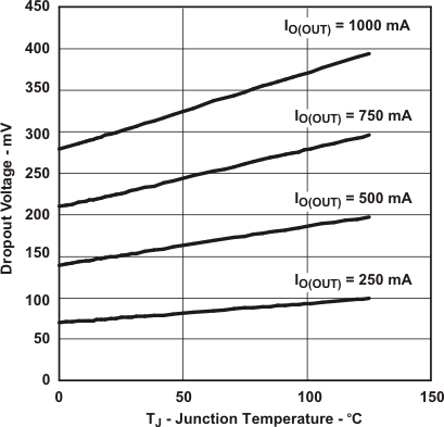 Figure 1. Dropout Voltage vs Junction Temperature
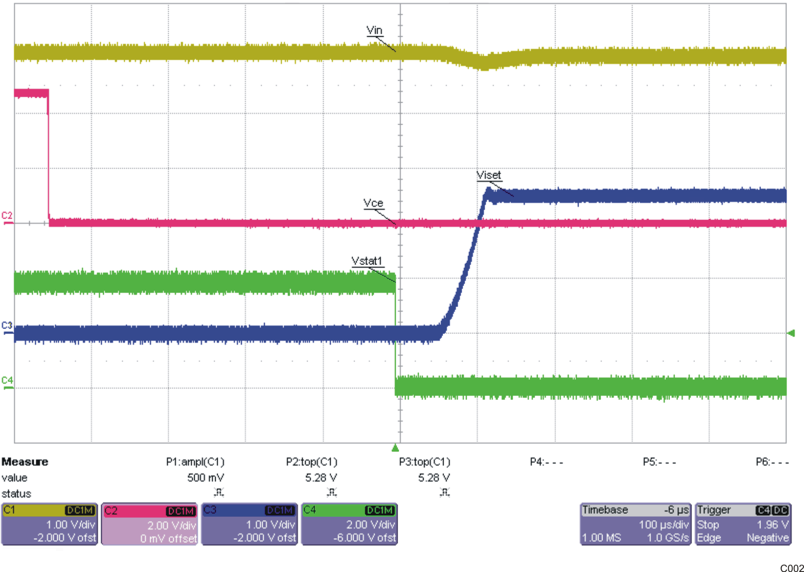 Figure 3. Charge Enable Power-Up Sequence
(CE = High-to-Low)
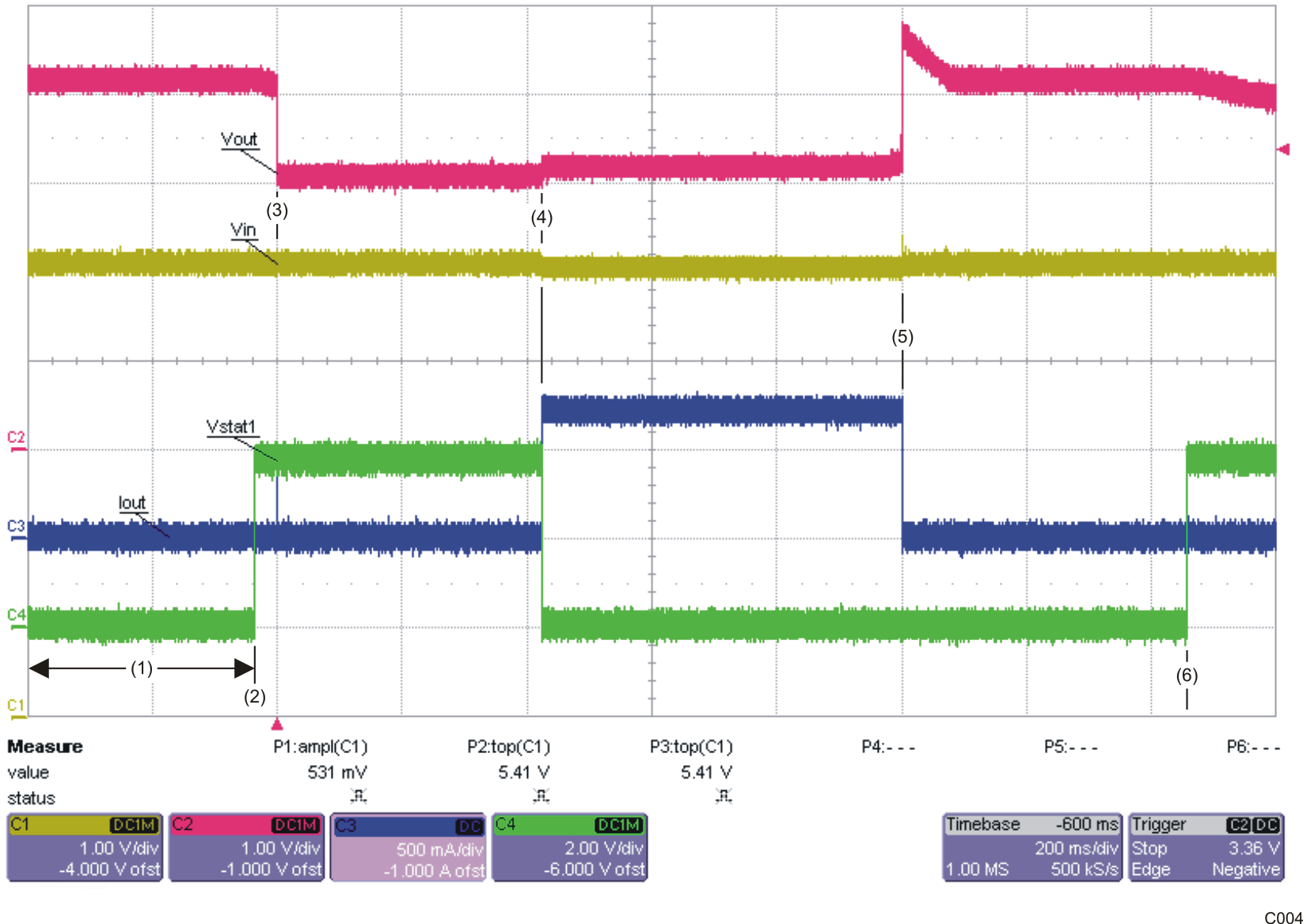
| No battery – In termination deglitch prior to STAT1 going high. VOUT (VBAT) cycling between charge and done prior to screen capture | ||
| Stat1 goes high – In done state | ||
| 2-V battery is inserted during the charge done state. | ||
| Charging is initiated – STAT1 goes low and charge current is applied. | ||
| Battery is removed – VOUT goes into regulation, IOUT goes to zero, and termination deglitch timer starts running (same as state 1). | ||
| Deglitch timer expires – charge done is declared. |
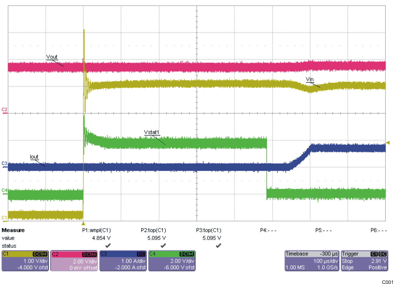
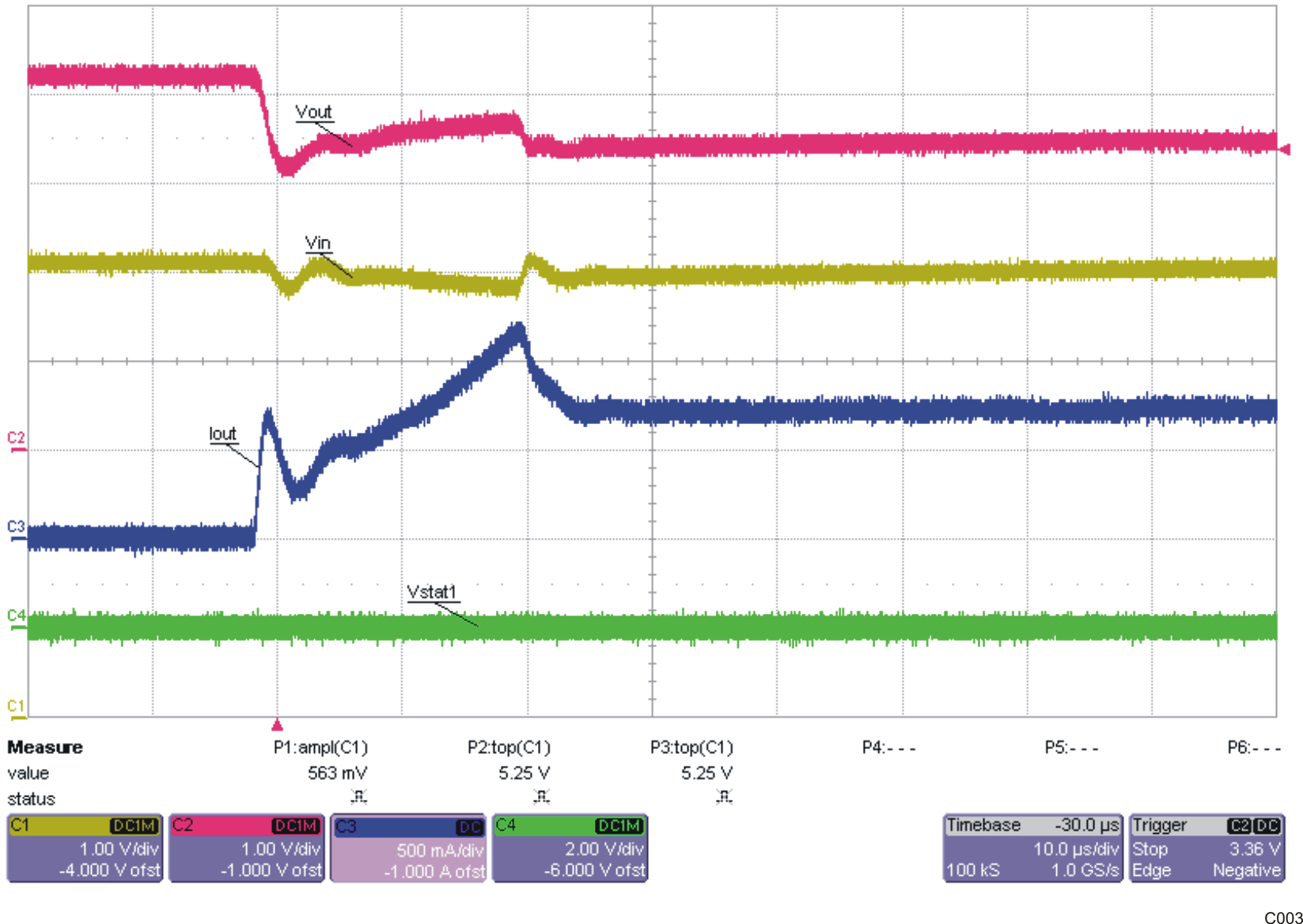 Figure 4. Battery Hot-Plug During Charging Phase