SLUSAB0D October 2010 – April 2016
UNLESS OTHERWISE NOTED, this document contains PRODUCTION DATA.
- 1 Features
- 2 Applications
- 3 Description
- 4 Revision History
- 5 Description (Continued)
- 6 Device Comparisons
- 7 Pin Configuration and Functions
- 8 Specifications
-
9 Detailed Description
- 9.1 Overview
- 9.2 Functional Block Diagram
- 9.3 Feature Description
- 9.4
Device Functional Modes
- 9.4.1 Charge Mode Operation
- 9.4.2 PWM Controller in Charge Mode
- 9.4.3 Battery Charging Process
- 9.4.4 Thermal Regulation and Protection
- 9.4.5 Charge Status Output, STAT Pin
- 9.4.6 Control Bits in Charge Mode
- 9.4.7 Control Pins in Charge Mode
- 9.4.8 BOOST Mode Operation (bq24153A/8 only)
- 9.4.9 High Impedance (HI-Z) Mode
- 9.5 Programming
- 9.6
Register Maps
- 9.6.1 Status/Control Register [Memory Location: 00, Reset State: x1xx 0xxx]
- 9.6.2 Control Register [Memory Location: 01, Reset State: 0011 0000]
- 9.6.3 Control/Battery Voltage Register [Memory Location: 02, Reset State: 0000 1010]
- 9.6.4 Vender/Part/Revision Register [Memory Location: 03, Reset State: 0101 000x]
- 9.6.5 Battery Termination/Fast Charge Current Register [Memory Location: 04, Reset State: 0000 000]
- 9.6.6 Special Charger Voltage/Enable Pin Status Register [Memory location: 05, Reset state: 001X X100]
- 9.6.7 Safety Limit Register [Memory location: 06, Reset state: 01000000]
- 10Application and Implementation
- 11Power Supply Recommendations
- 12Layout
- 13Device and Documentation Support
- 14Mechanical, Packaging, and Orderable Information
Package Options
Mechanical Data (Package|Pins)
- YFF|20
Thermal pad, mechanical data (Package|Pins)
Orderable Information
12 Layout
12.1 Layout Guidelines
It is important to pay special attention to the PCB layout. The following provides some guidelines:
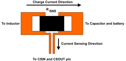
- To obtain optimal performance, the power input capacitors, connected from input to PGND, should be placed as close as possible to the pin. The output inductor should be placed close to the IC and the output capacitor connected between the inductor and PGND of the IC. The intent is to minimize the current path loop area from the SW pin through the LC filter and back to the PGND pin. To prevent high frequency oscillation problems, proper layout to minimize high frequency current path loop is critical. (See Figure 39.) The sense resistor should be adjacent to the junction of the inductor and output capacitor. Route the sense leads connected across the RSNS back to the IC, close to each other (minimize loop area) or on top of each other on adjacent layers (do not route the sense leads through a high-current path). (See Figure 40.)
- Place all decoupling capacitors close to their respective IC pins and close to PGND (do not place components such that routing interrupts power stage currents). All small control signals should be routed away from the high current paths.
- The PCB should have a ground plane (return) connected directly to the return of all components through vias (two vias per capacitor for power-stage capacitors, two vias for the IC PGND, one via per capacitor for small-signal components). A star ground design approach is typically used to keep circuit block currents isolated (high-power/low-power small-signal) which reduces noise-coupling and ground-bounce issues. A single ground plane for this design gives good results. With this small layout and a single ground plane, there is no ground-bounce issue, and having the components segregated minimizes coupling between signals.
- The high-current charge paths into VBUS, PMID and from the SW pins must be sized appropriately for the maximum charge current in order to avoid voltage drops in these traces. The PGND pins should be connected to the ground plane to return current through the internal low-side FET.
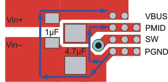
- Place 4.7μF input capacitor as close to PMID pin and PGND pin as possible to make high frequency current loop area as small as possible. Place 1μF input capacitor as close to VBUS pin and PGND pin as possible to make high frequency current loop area as small as possible (see Figure 41).
12.1.1 Current Path
 Figure 39. High Frequency Current Path
12.2 Layout Example
 Figure 40. Sensing Resistor PCB Layout
 Figure 41. Input Capacitor Position and PCB Layout Example