SLUSAB0D October   2010  – April 2016

UNLESS OTHERWISE NOTED, this document contains PRODUCTION DATA.  

  1. Features
  2. Applications
  3. Description
  4. Revision History
  5. Description (Continued)
  6. Device Comparisons
  7. Pin Configuration and Functions
  8. Specifications
    1. 8.1 Absolute Maximum Ratings
    2. 8.2 ESD Ratings
    3. 8.3 Recommended Operating Conditions
    4. 8.4 Thermal Information
    5. 8.5 Electrical Characteristics
    6. 8.6 Timing Requirements
    7. 8.7 Typical Characteristics
  9. Detailed Description
    1. 9.1 Overview
    2. 9.2 Functional Block Diagram
    3. 9.3 Feature Description
      1. 9.3.1 Input Voltage Protection
        1. 9.3.1.1 Input Overvoltage Protection
        2. 9.3.1.2 Bad Adaptor Detection/Rejection
        3. 9.3.1.3 Sleep Mode
        4. 9.3.1.4 Input Voltage Based DPM (Special Charger Voltage Threshold)
      2. 9.3.2 Battery Protection
        1. 9.3.2.1 Output Overvoltage Protection
        2. 9.3.2.2 Battery Short Protection
        3. 9.3.2.3 Battery Detection at Power Up in 15-minute Mode (bq24153A/6A only)
        4. 9.3.2.4 Battery Detection in Host Mode
      3. 9.3.3 15-Minute Safety Timer and 32-second Watchdog Timer in Charge Mode
      4. 9.3.4 USB Friendly Power Up
      5. 9.3.5 Input Current Limiting at Power Up
    4. 9.4 Device Functional Modes
      1. 9.4.1 Charge Mode Operation
        1. 9.4.1.1 Charge Profile
      2. 9.4.2 PWM Controller in Charge Mode
      3. 9.4.3 Battery Charging Process
      4. 9.4.4 Thermal Regulation and Protection
      5. 9.4.5 Charge Status Output, STAT Pin
      6. 9.4.6 Control Bits in Charge Mode
        1. 9.4.6.1 CE Bit (Charge Mode)
        2. 9.4.6.2 RESET Bit
        3. 9.4.6.3 OPA_Mode Bit
      7. 9.4.7 Control Pins in Charge Mode
        1. 9.4.7.1 CD Pin (Charge Disable)
        2. 9.4.7.2 SLRST Pin (Safety Limit Register 06H Reset, bq24156A/9 only)
      8. 9.4.8 BOOST Mode Operation (bq24153A/8 only)
        1. 9.4.8.1 PWM Controller in Boost Mode
        2. 9.4.8.2 Boost Start Up
        3. 9.4.8.3 PFM Mode at Light Load
        4. 9.4.8.4 Safety Timer in Boost Mode
        5. 9.4.8.5 Protection in Boost Mode
          1. 9.4.8.5.1 Output Overvoltage Protection
          2. 9.4.8.5.2 Output Overload Protection
          3. 9.4.8.5.3 Battery Overvoltage Protection
        6. 9.4.8.6 STAT Pin in Boost Mode
      9. 9.4.9 High Impedance (HI-Z) Mode
    5. 9.5 Programming
      1. 9.5.1 Serial Interface Description
        1. 9.5.1.1 F/S Mode Protocol
        2. 9.5.1.2 H/S Mode Protocol
        3. 9.5.1.3 I2C Update Sequence
        4. 9.5.1.4 Slave Address Byte
        5. 9.5.1.5 Register Address Byte
    6. 9.6 Register Maps
      1. 9.6.1 Status/Control Register [Memory Location: 00, Reset State: x1xx 0xxx]
      2. 9.6.2 Control Register [Memory Location: 01, Reset State: 0011 0000]
      3. 9.6.3 Control/Battery Voltage Register [Memory Location: 02, Reset State: 0000 1010]
      4. 9.6.4 Vender/Part/Revision Register [Memory Location: 03, Reset State: 0101 000x]
      5. 9.6.5 Battery Termination/Fast Charge Current Register [Memory Location: 04, Reset State: 0000 000]
      6. 9.6.6 Special Charger Voltage/Enable Pin Status Register [Memory location: 05, Reset state: 001X X100]
      7. 9.6.7 Safety Limit Register [Memory location: 06, Reset state: 01000000]
  10. 10Application and Implementation
    1. 10.1 Application Information
    2. 10.2 Typical Application
      1. 10.2.1 Design Requirements
      2. 10.2.2 Detailed Design Procedure
        1. 10.2.2.1 Systems Design Specifications
        2. 10.2.2.2 Charge Current Sensing Resistor Selection Guidelines
        3. 10.2.2.3 Output Inductor and Capacitance Selection Guidelines
      3. 10.2.3 Application Curves
    3. 10.3 System Example
  11. 11Power Supply Recommendations
    1. 11.1 System Load After Sensing Resistor
    2. 11.2 System Load Before Sensing Resistor
  12. 12Layout
    1. 12.1 Layout Guidelines
      1. 12.1.1 Current Path
    2. 12.2 Layout Example
  13. 13Device and Documentation Support
    1. 13.1 Third-Party Products Disclaimer
    2. 13.2 Related Links
    3. 13.3 Community Resources
    4. 13.4 Trademarks
    5. 13.5 Electrostatic Discharge Caution
    6. 13.6 Glossary
  14. 14Mechanical, Packaging, and Orderable Information
    1. 14.1 Package Summary
      1. 14.1.1 Chip Scale Packaging Dimensions

Package Options

Mechanical Data (Package|Pins)
Thermal pad, mechanical data (Package|Pins)
Orderable Information

7 Pin Configuration and Functions

YFF Package
20-Pin Bump DSBGA
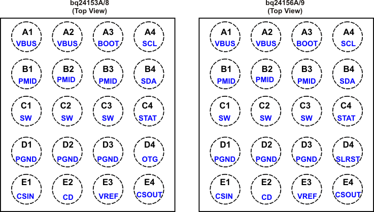
bq24153A bq24156A bq24158 bq24159 pins2_lusab0.gif

Pin Functions

PIN I/O DESCRIPTION
NAME NO.
BOOT A3 I/O Bootstrap capacitor connection for the high-side FET gate driver. Connect a 33-nF ceramic capacitor (voltage rating ≥ 10 V) from BOOT pin to SW pin.
CD E2 I Charge disable control pin. CD=0, charge is enabled. CD=1, charge is disabled and VBUS pin is high impedance to GND.
CSIN E1 I Charge current-sense input. Battery current is sensed across an external sense resistor. A 0.1-μF ceramic capacitor to PGND is required.
CSOUT E4 I Battery voltage and current sense input. Bypass it with a ceramic capacitor (minimum 0.1 μF) to PGND if there are long inductive leads to battery.
OTG
(bq24153A/8 only)
D4 I Boost mode enable control or input current limiting selection pin. When OTG is in active status, bq24153A/8 is forced to operate in boost mode. It has higher priority over I2C control and can be disabled using the control register. At POR while in 15-min mode, the OTG pin is default to be used as the input current limiting selection pin. The I2C register is ignored at startup. When OTG=High, IIN_LIMIT=500mA and when OTG=Low, IIN_LIMIT=100mA.
PGND D1, D2, D3 Power ground
PMID B1, B2, B3 I/O Connection point between reverse blocking FET and high-side switching FET. Bypass it with a minimum of 3.3-μF capacitor from PMID to PGND.
SCL A4 I I2C interface clock. Connect a 10-kΩ pullup resistor to 1.8V rail (VAUX= VCC_HOST)
SDA B4 I/O I2C interface data. Connect a 10-kΩ pullup resistor to 1.8V rail (VAUX= VCC_HOST)
SLRST
(bq24156A/9 only)
D4 I Safety limit register reset control. When SLRST=0, bq24156A/9 resets all the safety limits (06H) to default values, regardless of the write actions to safety limits registers (06H). When SLRST=1, bq24156A/9 can program the safety limit register until any write action to other registers locks the programmed safety limits.
STAT C4 O Charge status pin. Pull low when charge in progress. Open drain for other conditions. During faults, a 128-μs pulse is sent out. STAT pin can be disabled by the EN_STAT bit in control register. STAT can be used to drive a LED or communicate with a host processor.
SW C1, C2, C3 O Internal switch to output inductor connection.
VBUS A1, A2 I/O Charger input voltage. Bypass it with a 1-μF ceramic capacitor from VBUS to PGND. It also provides power to the load during boost mode (bq24153A/8 only) .
VREF E3 O Internal bias regulator voltage. Connect a 1µF ceramic capacitor from this output to PGND. External load on VREF is not recommended.