SLUSAO0H November 2011 – July 2022 BQ24160 , BQ24160A , BQ24161 , BQ24161B , BQ24163 , BQ24168
PRODUCTION DATA
- 1 Features
- 2 Applications
- 3 Description
- 4 Revision History
- 5 Device Comparison Table
- 6 Pin Configuration and Functions
- 7 Specifications
-
8 Detailed Description
- 8.1 Overview
- 8.2 Functional Block Diagram
- 8.3
Feature Description
- 8.3.1 Charge Mode Operation
- 8.3.2 Battery Charging Process
- 8.3.3 Battery Detection
- 8.3.4 Dynamic Power Path Management (DPPM)
- 8.3.5 Input Source Connected
- 8.3.6 Battery Only Connected
- 8.3.7 Battery Discharge FET (BGATE)
- 8.3.8 DEFAULT Mode
- 8.3.9 Safety Timer and Watchdog Timer (BQ24160/BQ24161/BQ24161B/BQ24163 only)
- 8.3.10 D+, D– Based Adapter Detection for the USB Input (D+, D–, BQ24160/0A/3)
- 8.3.11 USB Input Current Limit Selector Input (PSEL, BQ24161/161B/168 only)
- 8.3.12 Hardware Chip Disable Input (CD)
- 8.3.13 LDO Output (DRV)
- 8.3.14 External NTC Monitoring (TS)
- 8.3.15 Thermal Regulation and Protection
- 8.3.16 Input Voltage Protection in Charge Mode
- 8.3.17 Charge Status Outputs (STAT, INT)
- 8.3.18 Good Battery Monitor
- 8.4 Device Functional Modes
- 8.5 Programming
- 8.6
Register Maps
- 8.6.1 Status/Control Register (READ/WRITE)
- 8.6.2 Battery/ Supply Status Register (READ/WRITE)
- 8.6.3 Control Register (READ/WRITE)
- 8.6.4 Control/Battery Voltage Register (READ/WRITE)
- 8.6.5 Vender/Part/Revision Register (READ only)
- 8.6.6 Battery Termination/Fast Charge Current Register (READ/WRITE)
- 8.6.7 VIN-DPM Voltage/ DPPM Status Register
- 8.6.8 Safety Timer/ NTC Monitor Register (READ/WRITE)
- 9 Application and Implementation
- 10Power Supply Recommendations
- 11Layout
- 12Device and Documentation Support
Package Options
Mechanical Data (Package|Pins)
Thermal pad, mechanical data (Package|Pins)
- RGE|24
Orderable Information
8.3.16.5 Reverse Boost (Boost Back) Prevention Circuit
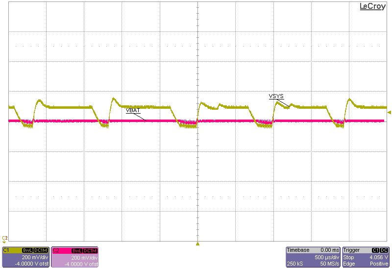
A buck converter has two operating modes, continuous conduction mode (CCM) and discontinuous conduction mode (DCM). In DCM, the inductor current ramps down to zero during the switching cycle while in CCM the inductor maintains a DC level of current. Transitioning from DCM to CCM during load transients, slows down the converter's transient response for those load steps, which can result in the SYS rail drooping. To achieve the fastest possible transient reponse for this charger, this charger's synchronous buck converter is forced to run in CCM even at light loads when the buck converter would typically revert to DCM. The challenge that presents itself when forcing CCM with a charger is that the output of the buck converter now has a power source. Thus, if the battery voltage, V(BAT), is ever greater than VBATREG, the inductor current goes fully negative and pushes current back to the input supply. This effect causes the input source voltage to rise if the input source cannot sink current. The input over-voltage protection circuit protects the IC from damage however some input sources may be damaged if the voltage rises. To prevent this, this charger has implemented a reverse boost prevention circuit. When reverse current is sensed that is not a result of the supplement comparator tripping, this circuit disables the internal battery FET and changes the feedback point to VSYSREG for 1 ms. After the 1-ms timeout, the BATFET is turned on again and the battery is tested to see if it is higher than VBATREG (negative current). The reverse current protection is only active when VBOVP > VBAT > VBATREG - VRCH. Having VBOVP > VBAT > VBATREG - VRCH results in an approximately 100-mV, 1000-Hz ripple on SYS as seen in Figure 8-7. The most common trigger for reverse boost prevention is a load transient on SYS that requires the charger to enter battery supplement mode. When the IC enters reverse boost prevention, the IC stops charging or exits charge done which may result in the battery never reaching full charge. With termination enabled and ITERM > 150 mA or with a high line impedance to the battery, the likelihood of activating the reverse boost prevention circuit is small and even when activated, the charger typically exits reverse boost prevention as the battery relaxes. With termination enabled and ITERM < 150 mA or with a low impedance battery, the likelihood of activating the reverse boost prevention circuit by a load transient or even the inductor ripple current is higher. In either case, the IC resumes charging until VBAT drops below VBATREG - VRCH, resulting in the battery always charging to at least 0.97 of full charge. If full charge is required with ITERM < 150 mA then the recommended solution to ensure full charge is as follows
1. SET the charger’s enable no battery operation bit ( EN_NOBATOP) = 1 to disable the reverse boost prevention circuits. Brief, low-amplitude voltage pulses on IN may be observed as the IC enters boost back to resolve instances where VBAT is greater than the VBATREG, for example when exiting supplement mode. The I2C communication software must ensure that VBATREG is never written below VBAT. The IC automatically rewrites the VBATREG register to the default value of 3.6 V when existing HOST mode. For JEITA enabled ICs, the IC automatically lowers the voltage reference to 0.98 of the VBATREG value. The software must account for these instances as well.
2. Disable the charger’s termination function and TS functions and use a gas gauge to control termination and TS through its independent voltage and current measurements.
 Figure 8-7 V(SYS) When Reverse Boost
Prevention Circuit is Active