SLUSBP6D september   2013  ā€“ april 2023 BQ24296 , BQ24297

PRODUCTION DATA  

  1. Features
  2. Applications
  3. Description
  4. Revision History
  5. Description (continued)
  6. Device Comparison Table
  7. Pin Configuration and Functions
  8. Specifications
    1. 8.1 Absolute Maximum Ratings #GUID-BA2DB09A-966C-4324-B633-1AB165FC219B/SLUSBC14058
    2. 8.2 ESD Ratings
    3. 8.3 Recommended Operating Conditions
    4. 8.4 Thermal Information
    5. 8.5 Electrical Characteristics
    6. 8.6 Timing Requirements
    7. 8.7 Typical Characteristics
  9. Detailed Description
    1. 9.1 Overview
    2. 9.2 Functional Block Diagram
    3. 9.3 Feature Description
      1. 9.3.1 Device Power Up
        1. 9.3.1.1 Power-On-Reset (POR)
        2. 9.3.1.2 Power Up from Battery without DC Source
          1. 9.3.1.2.1 BATFET Turn Off
          2. 9.3.1.2.2 Shipping Mode
        3. 9.3.1.3 Power Up from DC Source
          1. 9.3.1.3.1 REGN LDO
          2. 9.3.1.3.2 Input Source Qualification
          3. 9.3.1.3.3 Input Current Limit Detection
          4. 9.3.1.3.4 D+/Dā€“ Detection Sets Input Current Limit (BQ24297)
          5. 9.3.1.3.5 PSEL/OTG Pins Set Input Current Limit
          6. 9.3.1.3.6 HIZ State with 100mA USB Host
          7. 9.3.1.3.7 Force Input Current Limit Detection
        4. 9.3.1.4 Converter Power-Up
        5. 9.3.1.5 Boost Mode Operation from Battery
      2. 9.3.2 Power Path Management
        1. 9.3.2.1 Narrow VDC Architecture
        2. 9.3.2.2 Dynamic Power Management
        3. 9.3.2.3 Supplement Mode
      3. 9.3.3 Battery Charging Management
        1. 9.3.3.1 Autonomous Charging Cycle
        2. 9.3.3.2 Battery Charging Profile
        3. 9.3.3.3 Thermistor Qualification
          1. 9.3.3.3.1 Cold/Hot Temperature Window
        4. 9.3.3.4 Charging Termination
          1. 9.3.3.4.1 Termination When REG02[0] = 1
        5. 9.3.3.5 Charging Safety Timer
          1. 9.3.3.5.1 Safety Timer Configuration Change
        6. 9.3.3.6 USB Timer When Charging from USB100mA Source
      4. 9.3.4 Status Outputs ( PG, STAT, and INT)
        1. 9.3.4.1 Power Good Indicator ( PG) (BQ24296)
        2. 9.3.4.2 Charging Status Indicator (STAT)
        3. 9.3.4.3 Interrupt to Host (INT)
      5. 9.3.5 Protections
        1. 9.3.5.1 Input Current Limit on ILIM
        2. 9.3.5.2 Thermal Regulation and Thermal Shutdown
        3. 9.3.5.3 Voltage and Current Monitoring in Buck Mode
          1. 9.3.5.3.1 Input Over-Voltage (ACOV)
          2. 9.3.5.3.2 System Over-Voltage Protection (SYSOVP)
        4. 9.3.5.4 Voltage and Current Monitoring in Boost Mode
          1. 9.3.5.4.1 Over-Current Protection
          2. 9.3.5.4.2 VBUS Over-Voltage Protection
        5. 9.3.5.5 Battery Protection
          1. 9.3.5.5.1 Battery Over-Voltage Protection (BATOVP)
          2. 9.3.5.5.2 Battery Short Protection
          3. 9.3.5.5.3 System Over-Current Protection
    4. 9.4 Device Functional Modes
      1. 9.4.1 Host Mode and Default Mode
        1. 9.4.1.1 Plug in USB100mA Source with Good Battery
        2. 9.4.1.2 USB Timer When Charging from USB100mA Source
    5. 9.5 Programming
      1. 9.5.1 Serial Interface
        1. 9.5.1.1 Data Validity
        2. 9.5.1.2 START and STOP Conditions
        3. 9.5.1.3 Byte Format
        4. 9.5.1.4 Acknowledge (ACK) and Not Acknowledge (NACK)
        5. 9.5.1.5 Target Address and Data Direction Bit
          1. 9.5.1.5.1 Single Read and Write
          2. 9.5.1.5.2 Multi-Read and Multi-Write
    6. 9.6 Register Map
      1. 9.6.1 I2C Registers
        1. 9.6.1.1  Input Source Control Register REG00 [reset = 00110xxx, or 3x]
        2. 9.6.1.2  Power-On Configuration Register REG01 [reset = 00011011, or 0x1B]
        3. 9.6.1.3  Charge Current Control Register REG02 [reset = 01100000, or 60]
        4. 9.6.1.4  Pre-Charge/Termination Current Control Register REG03 [reset = 00010001, or 0x11]
        5. 9.6.1.5  Charge Voltage Control Register REG04 [reset = 10110010, or 0xB2]
        6. 9.6.1.6  Charge Termination/Timer Control Register REG05 [reset = 10011010, or 0x9A]
        7. 9.6.1.7  Boost Voltage/Thermal Regulation Control Register REG06 [reset = 01110011, or 0x73]
        8. 9.6.1.8  Misc Operation Control Register REG07 [reset = 01001011, or 4B]
        9. 9.6.1.9  System Status Register REG08
        10. 9.6.1.10 New Fault Register REG09
        11. 9.6.1.11 Vender / Part / Revision Status Register REG0A
  10. 10Application and Implementation
    1. 10.1 Application Information
    2. 10.2 Typical Application
      1. 10.2.1 Design Requirements
      2. 10.2.2 Detailed Design Procedure
        1. 10.2.2.1 Inductor Selection
        2. 10.2.2.2 Input Capacitor
        3. 10.2.2.3 Output Capacitor
      3. 10.2.3 Application Performance Plots
  11. 11Power Supply Recommendations
  12. 12Layout
    1. 12.1 Layout Guidelines
    2. 12.2 Layout Example
  13. 13Device and Documentation Support
    1. 13.1 Device Support
      1. 13.1.1 Third-Party Products Disclaimer
    2. 13.2 Documentation Support
      1. 13.2.1 Related Documentation
    3. 13.3 Receiving Notification of Documentation Updates
    4. 13.4 Support Resources
    5. 13.5 Trademarks
    6. 13.6 Electrostatic Discharge Caution
    7. 13.7 Glossary
  14. 14Mechanical, Packaging, and Orderable Information

Package Options

Mechanical Data (Package|Pins)
Thermal pad, mechanical data (Package|Pins)
Orderable Information

Narrow VDC Architecture

The device deploys Narrow VDC architecture (NVDC) with BATFET separating system from battery. The minimum system voltage is set by REG01[3:1]. Even with a fully depleted battery, the system is regulated above the minimum system voltage (default 3.5 V).

When the battery is below minimum system voltage setting, the BATFET operates in linear mode (LDO mode), and the system is 150 mV above the minimum system voltage setting. As the battery voltage rises above the minimum system voltage, BATFET is fully on and the voltage difference between the system and battery is the VDS of BATFET.

When the battery charging is disabled or terminated, the system is always regulated at 150 mV above the minimum system voltage setting. The status register REG08[0] goes high when the system is in minimum system voltage regulation.
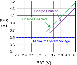
GUID-299C1544-77E0-47F5-9E3E-5C4A95C28886-low.gifFigure 9-3 V(SYS) vs V(BAT)