SLUSBT8 July 2014
PRODUCTION DATA.
- 1 Features
- 2 Applications
- 3 Description
- 4 Application Information
- 5 Revision History
- 6 Pin Configuration and Functions
- 7 Specifications
- 8 Detailed Description
- 9 Application and Implementation
- 10Power Supply Requirements
- 11Layout
- 12Device and Documentation Support
- 13Mechanical, Packaging, and Orderable Information
Package Options
Mechanical Data (Package|Pins)
- DSG|8
Thermal pad, mechanical data (Package|Pins)
- DSG|8
Orderable Information
6 Pin Configuration and Functions
DSG PACKAGE
(TOP VIEW)
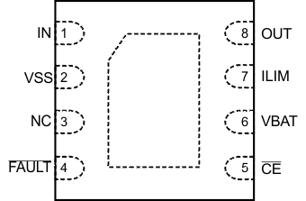
Pin Functions
| PIN | I/O | DESCRIPTION | ||
|---|---|---|---|---|
| NAME | DSG | |||
| IN | 1 | I | Input power, connect to external DC supply. Connect external 1μF ceramic capacitor (minimum) to VSS. | |
| OUT | 8 | O | Output pin to the charging system. Connect external 1 μF ceramic capacitor (minimum) to VSS. | |
| VBAT | 6 | I | Battery voltage sense input. Connect to pack positive pin through a resistor. | |
| ILIM | 7 | I/O | Input overcurrent threshold programming. Connect a resistor to VSS to set the overcurrent threshold. | |
| CE | 5 | I | Chip enable input. Active low. When CE = High, the input FET is off. Internally pulled down. | |
| FAULT | 4 | O | Device status, open-drain output. FAULT = Low indicates that the input FET Q1 has been turned on due to input overvoltage, input overcurrent, battery overvoltage, or thermal shutdown. | |
| VSS | 2 | – | Ground pin | |
| NC | 3 | This pin may have internal circuits used for test purposes. Do not make any external connections at these pins for normal operation. | ||
| Thermal PAD | – | There is an internal electrical connection between the exposed thermal pad and the VSS pin of the device. The thermal pad must be connected to the same potential as the VSS pin on the printed circuit board. Do not use the thermal pad as the primary ground input for the device. The VSS pin must be connected to ground at all times. | ||