SLUSBT8 July 2014
PRODUCTION DATA.
- 1 Features
- 2 Applications
- 3 Description
- 4 Application Information
- 5 Revision History
- 6 Pin Configuration and Functions
- 7 Specifications
- 8 Detailed Description
- 9 Application and Implementation
- 10Power Supply Requirements
- 11Layout
- 12Device and Documentation Support
- 13Mechanical, Packaging, and Orderable Information
Package Options
Mechanical Data (Package|Pins)
- DSG|8
Thermal pad, mechanical data (Package|Pins)
- DSG|8
Orderable Information
7 Specifications
7.1 Absolute Maximum Ratings(1)
over operating free-air temperature range (unless otherwise noted)| PARAMETER | MIN | MAX | UNIT | |
|---|---|---|---|---|
| Input voltage | IN (with respect to VSS) | –0.3 | 30 | V |
| OUT (with respect to VSS) | –0.3 | 12 | ||
| ILIM, FAULT, CE, VBAT (with respect to VSS) | –0.3 | 7 | ||
| Input current | IN | 0.5 | A | |
| Output current | OUT | 0.5 | A | |
| Output sink current | FAULT | 15 | mA | |
| Junction temperature, TJ | –40 | 150 | °C |
7.2 Handling Ratings
| MIN | MAX | UNIT | |||
|---|---|---|---|---|---|
| Tstg | Storage temperature range | –65 | 150 | °C | |
| VESD | Electrostatic discharge | Human body model (HBM), per ANSI/ESDA/JEDEC JS-001, all pins(1) | –2000 | 2000 | V |
| Charged device model (CDM), per JEDEC specification JESD22-C101, all pins (2) | –500 | 500 | V | ||
(1) JEDEC document JEP155 states that 500-V HBM allows safe manufacturing with a standard ESD control process.
(2) (2) JEDEC document JEP157 states that 250-V CDM allows safe manufacturing with a standard ESD control process.
7.3 Recommended Operating Conditions
over operating free-air temperature range (unless otherwise noted)| MIN | MAX | UNIT | ||
|---|---|---|---|---|
| VIN | Input voltage range | 3 | 26 | V |
| IIN | Input current, IN pin | 50 | 300 | mA |
| IOUT | Output current, OUT pin | 50 | 300 | mA |
| RILIM | OCP Programming resistor | 83.3 | 500 | kΩ |
| TJ | Junction temperature | –40 | 125 | °C |
7.4 Thermal Information
| THERMAL METRIC(1) | DSG | UNITS | |
|---|---|---|---|
| 8 PINS | |||
| RθJA | Junction-to-ambient thermal resistance | 86.3 | °C/W |
| RθJCtop | Junction-to-case (top) thermal resistance | 116.9 | |
| RθJB | Junction-to-board thermal resistance | 56.1 | |
| ψJT | Junction-to-top characterization parameter | 8.1 | |
| ψJB | Junction-to-board characterization parameter | 56.4 | |
| RθJCbot | Junction-to-case (bottom) thermal resistance | 25.9 | |
(1) For more information about traditional and new thermal metrics, see the IC Package Thermal Metrics application report, SPRA953.
7.5 Electrical Characteristics
over junction temperature range –40°C to 125°C and recommended supply voltage (unless otherwise noted)| PARAMETER | TEST CONDITIONS | MIN | TYP | MAX | UNIT | |||
|---|---|---|---|---|---|---|---|---|
| IN | ||||||||
| V(UVLO) | Undervoltage lock-out, input power detected threshold | CE = Low, VIN increasing from 0 V to 3 V | 2.6 | 2.7 | 2.8 | V | ||
| V(UVLO_HYS) | Hysteresis on UVLO | CE = Low, VIN decreasing from 3 V to 0 V | 200 | 260 | 300 | mV | ||
| IDD | Operating current | CE = Low, No load on OUT pin, VIN = 5 V, R(ILIM) = 200 kΩ |
400 | 500 | μA | |||
| I(STDBY) | Standby current | CE = High, VIN = 5 V | 65 | 95 | μA | |||
| INPUT TO OUTPUT CHARACTERISTICS | ||||||||
| V(DO) | Drop-out voltage IN to OUT | CE = Low, VIN = 5 V, IOUT = 0.125 A | 21 | 35 | mV | |||
| INPUT OVERVOLTAGE PROTECTION | ||||||||
| V(OVP) | Input overvoltage protection threshold | CE = Low, VIN increasing from 5V to 7.5 V | 5.71 | 5.85 | 6.00 | V | ||
| VHYS-OVP | Hysteresis on OVP | CE = Low, VIN decreasing from 7.5 V to 5 V | 20 | 60 | 110 | mV | ||
| INPUT OVERCURRENT PROTECTION | ||||||||
| I(OCP) | Input overcurrent protection threshold range | 50 | 300 | mA | ||||
| Input overcurrent protection threshold | CE = Low, RILIM = 200 kΩ, 3 V ≤ VIN < VOVP |
TJ = 0°C to 85°C | 110 | 125 | 135 | mA | ||
| TJ = 0°C to 125°C | 110 | 125 | 140 | |||||
| BATTERY OVERVOLTAGE PROTECTION | ||||||||
| V(BOVP) | Battery overvoltage protection threshold | CE = Low, VIN > 4.4 V | 4.30 | 4.35 | 4.4 | V | ||
| V(HYS-BOVP) | Hysteresis on V(BOVP) | CE = Low, VIN > 4.4 V | 200 | 275 | 320 | mV | ||
| I(VBAT) | Input bias current on VBAT pin | VBAT = 4.4 V, TJ = 25°C | 10 | nA | ||||
| THERMAL PROTECTION | ||||||||
| TJ(OFF) | Thermal shutdown temperature | 140 | 150 | °C | ||||
| TJ(OFF-HYS) | Thermal shutdown hysteresis | 20 | °C | |||||
| LOGIC LEVELS ON CE | ||||||||
| VIL | Low-level input voltage | 0 | 0.4 | V | ||||
| VIH | High-level input voltage | 1.4 | V | |||||
| IIL | Low-level input current | VCE = 0 V | 1 | μA | ||||
| IIH | High-level input current | VCE = 1.8 V | 15 | μA | ||||
| LOGIC LEVELS ON FAULT | ||||||||
| VOL | Output low voltage | I(SINK) = 5 mA | 0.2 | V | ||||
| I(HI-Z) | Leakage current, FAULT pin HI-Z | V(FAULT) = 5 V | 10 | μA | ||||
(1) Not tested in production. Specified by design.
7.6 Timing Requirements
| MIN | TYP | MAX | UNIT | |||
|---|---|---|---|---|---|---|
| tDGL(PGOOD) | Deglitch time, input power detected status | CE = Low. Time measured from VIN 0 V → 5 V 1 μs rise-time, to output turning ON | 8 | ms | ||
| tPD(OVP) | Input OV propagation delay(1) | CE = Low | 1 | μs | ||
| tON(OVP) | Recovery time from input overvoltage condition | CE = Low, Time measured from VIN 7.5 V → 5 V, 1μs fall-time |
8 | ms | ||
| tBLANK(OCP) | Blanking time, input overcurrent detected | 176 | μs | |||
| tREC(OCP) | Recovery time from input overcurrent condition | 64 | ms | |||
| tDGL(BOVP) | Deglitch time, battery overvoltage detected | CE = Low, VIN > 4.4 V. Time measured from V(VBAT) rising from 4.1 V to 4.4 V to FAULT going low. | 176 | μs | ||
7.7 Typical Characteristics
Test conditions (unless otherwise noted) for typical operating performance: VIN = 5 V, CIN = 1 μF, COUT = 1 μF, R(ILIM) = 200 kΩ, R(BAT) = 100 kΩ, TA = 25°C, V(PU) = 3.3 V (see Figure 11 for the Typical Application Circuit)
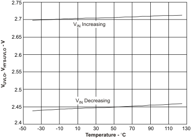
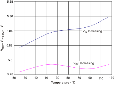
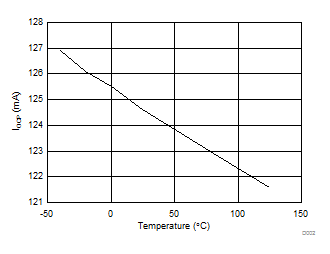 Figure 5. Input Overcurrent Protection vs Free-Air Temperature
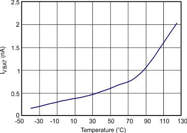
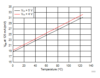
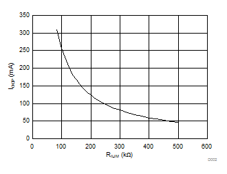
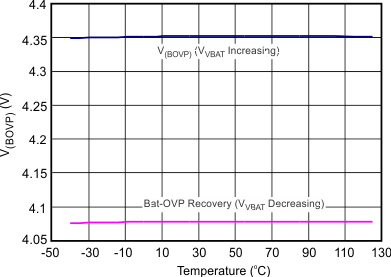 Figure 6. Battery Overvoltage Protection vs Free-Air Temperature
