SLUSC03C August 2014 – December 2016
PRODUCTION DATA.
- 1 Features
- 2 Applications
- 3 Description
- 4 Revision History
- 5 Device Comparison Table
- 6 Pin Configuration and Functions
- 7 Specifications
-
8 Detailed Description
- 8.1 Overview
- 8.2 Functional Block Diagram
- 8.3 Feature Description
- 8.4 Device Functional Modes
- 8.5 Programming
- 8.6 Register Maps
- 9 Application and Implementation
- 10Power Supply Recommendations
- 11Layout
- 12Device and Documentation Support
- 13Mechanical, Packaging, and Orderable Information
Package Options
Mechanical Data (Package|Pins)
- RUY|28
Thermal pad, mechanical data (Package|Pins)
Orderable Information
9 Application and Implementation
NOTE
Information in the following applications sections is not part of the TI component specification, and TI does not warrant its accuracy or completeness. TI’s customers are responsible for determining suitability of components for their purposes. Customers should validate and test their design implementation to confirm system functionality.
9.1 Application Information
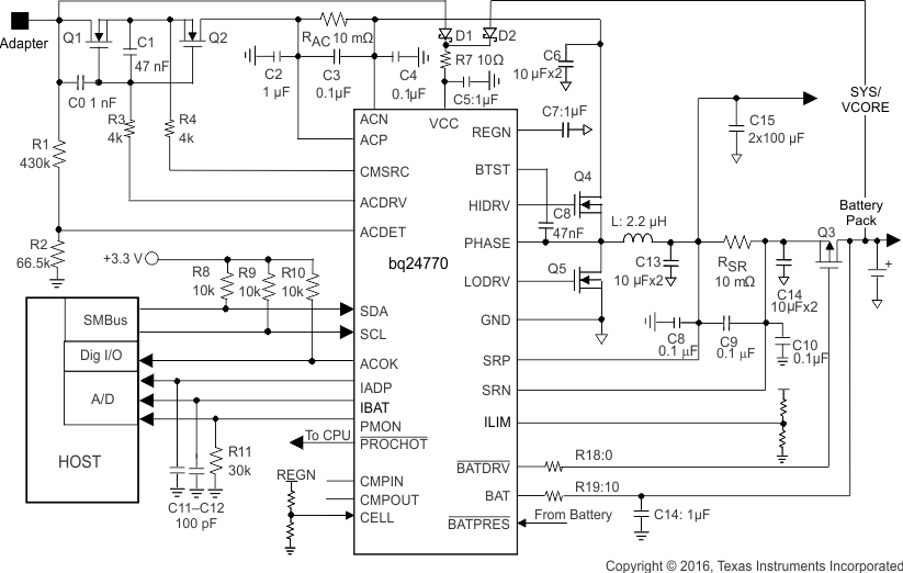
The bq2477xEVM-540 evaluation module (EVM) is a complete charger module for evaluating the bq2477x. The application curves were taken using the bq24770EVM-540. Refer to the EVM user's guide (SLUUAO3) for EVM information.
9.2 Typical Application, bq24770
9.2.1 Design Requirements
| DESIGN PARAMETER | EXAMPLE VALUE |
|---|---|
| Input Voltage(2) | 17.7V < Adapter Voltage < 24V |
| Input Current Limit (2) | 3.2A for 65W adapter |
| Battery Charge Voltage(1) | 8400mV for 2s battery |
| Battery Charge Current(1) | 4096mA for 3s battery |
| Minimum System Voltage(1) | 6144mA for 2s battery |
9.2.2 Detailed Design Procedure
The parameters are configurable using the evaluation software.
The simplified application circuit (see Figure 21) shows the minimum capacitance requirements for each pin. Inductor, capacitor, and MOSFET selection are explained in the rest of this section. Refer to the EVM user's guide (SLUUAO3) for the full application schematic.
9.2.2.1 Reverse Input Voltage Protection
Q6, R12, and R13 in Figure 22 give system and IC protection from reversed adapter voltage. In normal operation, Q6 is turned off by negative Vgs. When adapter voltage is reversed, Q6 Vgs is positive. As a result, Q6 turns on to short gate and source of Q2 so that Q2 is off. Q2 body diode blocks negative voltage to system. However, CMSRC and ACDRV pins need R3 and R4 to limit the current due to the ESD diode of these pins when turned on. Q6 must has low Vgs threshold voltage and low Qgs gate charge so it turns on before Q2 turns on. R3 and R4 must have enough power rating for the power dissipation when the ESD diode is on. If Q1 is replaced by Schottky diode for reverse adapter voltage protection, no extra small MOSFET and resistors are needed.
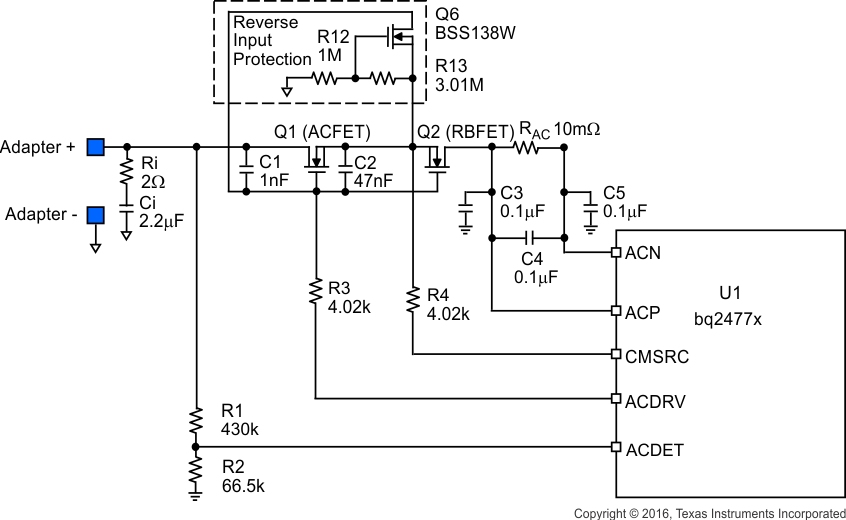 Figure 22. Reverse Input Voltage Protection Circuit
9.2.2.2 Inductor Selection
The bq2477x has three selectable fixed switching frequency. Higher switching frequency allows the use of smaller inductor and capacitor values. Inductor saturation current should be higher than the charging current (ICHG) plus half the ripple current (IRIPPLE):

The inductor ripple current depends on input voltage (VIN), duty cycle (D = VOUT/VIN), switching frequency (fS) and inductance (L):

The maximum inductor ripple current happens with D = 0.5 or close to 0.5. For example, the battery charging voltage range is from 9V to 12.6V for 3-cell battery pack. For 20 V adapter voltage, 10 V battery voltage gives the maximum inductor ripple current. Another example is 4-cell battery, the battery voltage range is from 12 V to 16.8 V, and 12 V battery voltage gives the maximum inductor ripple current.
Usually inductor ripple is designed in the range of (20-40%) maximum charging current as a trade-off between inductor size and efficiency for a practical design.
9.2.2.3 Input Capacitor
Input capacitor should have enough ripple current rating to absorb input switching ripple current. The worst case RMS ripple current is half of the charging current when duty cycle is 0.5. If the converter does not operate at 50% duty cycle, then the worst case capacitor RMS current occurs where the duty cycle is closest to 50% and can be estimated by Equation 4:

Low ESR ceramic capacitor such as X7R or X5R is preferred for input decoupling capacitor and should be placed to the drain of the high side MOSFET and source of the low side MOSFET as close as possible. Voltage rating of the capacitor must be higher than normal input voltage level. 25 V rating or higher capacitor is preferred for 19-20 V input voltage. 10-20 μF capacitance is suggested for typical of 3-4 A charging current.
Ceramic capacitors show a dc-bias effect. This effect reduces the effective capacitance when a dc-bias voltage is applied across a ceramic capacitor, as on the input capacitor of a charger. The effect may lead to a significant capacitance drop, especially for high input voltages and small capacitor packages. See the manufacturer's datasheet about the performance with a dc bias voltage applied. It may be necessary to choose a higher voltage rating or nominal capacitance value in order to get the required value at the operating point.
9.2.2.4 Output Capacitor
Output capacitor also should have enough ripple current rating to absorb output switching ripple current. The output capacitor RMS current is given:

The bq2477x has internal loop compensator. To get good loop stability, the resonant frequency of the output inductor and output capacitor should be designed between 10 kHz and 20 kHz. The preferred ceramic capacitor is 25V X7R or X5R for output capacitor. 10-20μF capacitance is suggested for a typical of 3-4A charging current. Place the capacitors after charging current sensing resistor to get the best charge current regulation accuracy.
Ceramic capacitors show a dc-bias effect. This effect reduces the effective capacitance when a dc-bias voltage is applied across a ceramic capacitor, as on the output capacitor of a charger. The effect may lead to a significant capacitance drop, especially for high output voltages and small capacitor packages. See the manufacturer's data sheet about the performance with a dc bias voltage applied. It may be necessary to choose a higher voltage rating or nominal capacitance value in order to get the required value at the operating point.
9.2.2.5 Power MOSFETs Selection
Two external N-channel MOSFETs are used for a synchronous switching battery charger. The gate drivers are internally integrated into the IC with 6V of gate drive voltage. 30 V or higher voltage rating MOSFETs are preferred for 19-20 V input voltage.
Figure-of-merit (FOM) is usually used for selecting proper MOSFET based on a tradeoff between the conduction loss and switching loss. For the top side MOSFET, FOM is defined as the product of a MOSFET's on-resistance, RDS(ON), and the gate-to-drain charge, QGD. For the bottom side MOSFET, FOM is defined as the product of the MOSFET's on-resistance, RDS(ON), and the total gate charge, QG.
The lower the FOM value, the lower the total power loss. Usually lower RDS(ON) has higher cost with the same package size.
The top-side MOSFET loss includes conduction loss and switching loss. It is a function of duty cycle (D=VOUT/VIN), charging current (ICHG), MOSFET's on-resistance (RDS(ON)), input voltage (VIN), switching frequency (fS), turn on time (ton) and turn off time (toff):

The first item represents the conduction loss. Usually MOSFET RDS(ON) increases by 50% with 100°C junction temperature rise. The second term represents the switching loss. The MOSFET turn-on and turn-off times are given by:

where Qsw is the switching charge, Ion is the turn-on gate driving current and Ioff is the turn-off gate driving current. If the switching charge is not given in MOSFET datasheet, it can be estimated by gate-to-drain charge (QGD) and gate-to-source charge (QGS):

Gate driving current can be estimated by REGN voltage (VREGN), MOSFET plateau voltage (Vplt), total turn-on gate resistance (Ron) and turn-off gate resistance (Roff) of the gate driver:

The conduction loss of the bottom-side MOSFET is calculated with the following equation when it operates in synchronous continuous conduction mode:
When charger operates in non-synchronous mode, the bottom-side MOSFET is off. As a result all the freewheeling current goes through the body-diode of the bottom-side MOSFET. The body diode power loss depends on its forward voltage drop (VF), non-synchronous mode charging current (INONSYNC), and duty cycle (D).
The maximum charging current in non-synchronous mode can be up to 0.25 A for a 10 mΩ charging current sensing resistor or 0.5 A if battery voltage is below 2.5 V. The minimum duty cycle happens at lowest battery voltage. Choose the bottom-side MOSFET with either an internal Schottky or body diode capable of carrying the maximum non-synchronous mode charging current.
9.2.2.6 Input Filter Design
During adapter hot plug-in, the parasitic inductance and input capacitor from the adapter cable form a second order system. The voltage spike at VCC pin maybe beyond IC maximum voltage rating and damage IC. The input filter must be carefully designed and tested to prevent over voltage event on VCC pin.
There are several methods to damping or limit the over voltage spike during adapter hot plug-in. An electrolytic capacitor with high ESR as an input capacitor can damp the over voltage spike well below the IC maximum pin voltage rating. A high current capability TVS Zener diode can also limit the over voltage level to an IC safe level. However these two solutions may not have low cost or small size.
A cost effective and small size solution is shown in Figure 23. The R1 and C1 are composed of a damping RC network to damp the hot plug-in oscillation. As a result the over voltage spike is limited to a safe level. D1 is used for reverse voltage protection for VCC pin. C2 is VCC pin decoupling capacitor and it should be place to VCC pin as close as possible. C2 value should be less than C1 value so R1 can dominant the equivalent ESR value to get enough damping effect. R2 is used to limit inrush current of D1 to prevent D1 getting damage when adapter hot plug-in. R2 and C2 should have 10 µs time constant to limit the dv/dt on VCC pin to reduce inrush current when adapter hot plug in. R1 has high inrush current. R1 package must be sized enough to handle inrush current power loss according to resistor manufacturer’s data sheet. The filter components value always need to be verified with real application and minor adjustments may need to fit in the real application circuit.
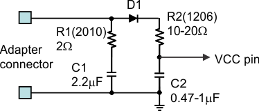 Figure 23. Input Filter
9.2.3 Application Curves
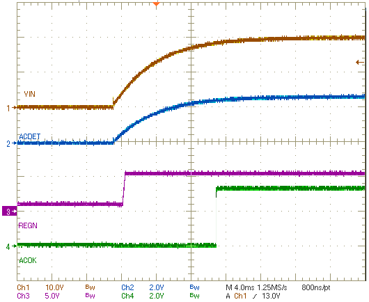
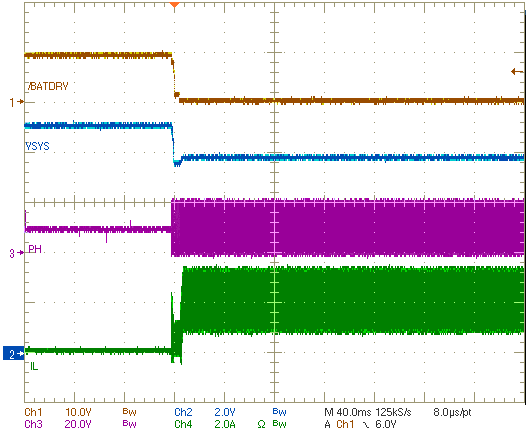
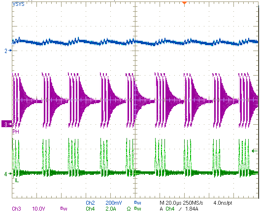
| VIN = 19.5 V | I(SYS) = 200 mA | CELL = Float |
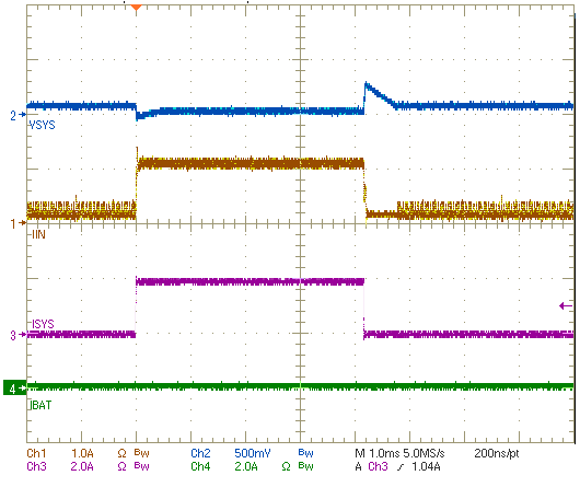
| VIN = 19.5 V | CELL = Float |
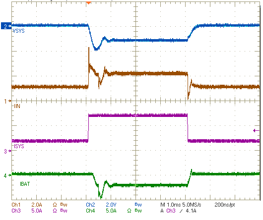
| VIN = 19.5 V | CELL = Float |
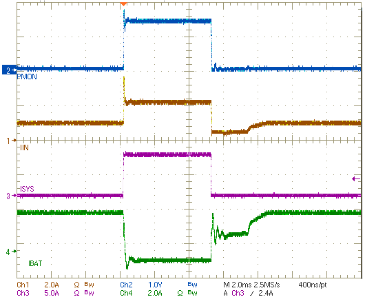
| VIN = 19.5 V | CELL = Float | VBAT 7.5 V |
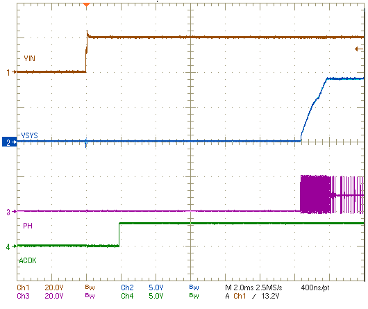
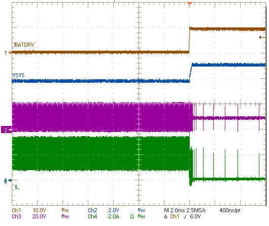
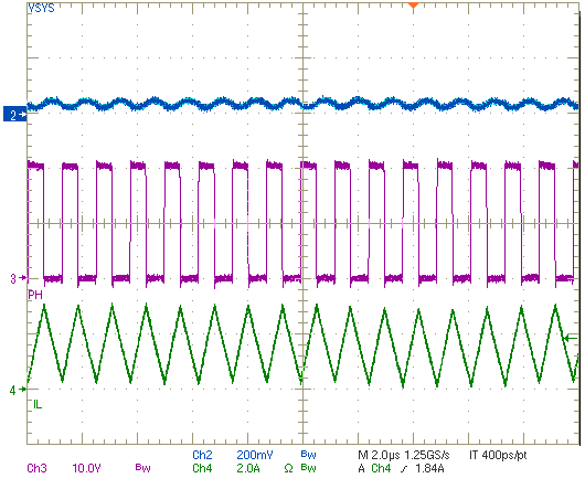
| VIN = 19.5 V | I(SYS) = 1.5 A | CELL = Float |
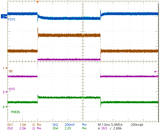
| VIN = 19.5 V | CELL = Float |
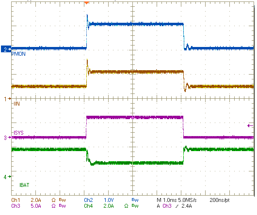
| VIN = 19.5 V | CELL = Float | VBAT 7.5 V |
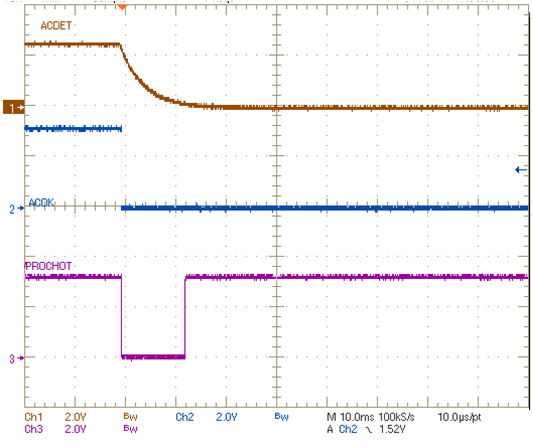
| IDPM 3072 mA | ICHG 2432mA | VBAT 11 V |
| ICRIT 150% × IDPM | ||
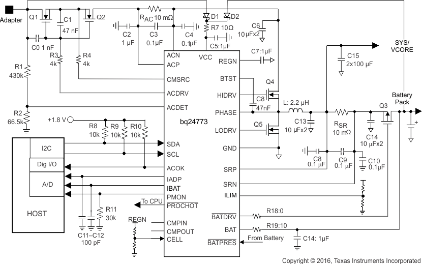
9.2.4 Typical Application, bq24773
The bq2477xEVM-540 evaluation module (EVM) is a complete charger module for evaluating the bq2477x. The application curves were taken using the bq24770EVM-540. Refer to the EVM user's guide (SLUUAO3) for EVM information.
9.2.4.1 Design Requirements
Refer to Typical Application, bq24770 for the Design Requirements.
9.2.4.2 Detailed Design Procedure
Refer to Typical Application, bq24770 for the Detailed Design Procedure.
9.2.4.3 Application Curves
Refer to Typical Application, bq24770 for the Application Curves.
