SLUSBK6 July 2014
PRODUCTION DATA.
- 1 Features
- 2 Applications
- 3 Description
- 4 Application Schematic
- 5 Revision History
- 6 Device Comparison Table
- 7 Pin Configuration and Functions
- 8 Specifications
- 9 Detailed Description
- 10Application and Implementation
- 11Power Supply Recommendations
- 12Layout
- 13Device and Documentation Support
- 14Mechanical, Packaging, and Orderable Information
Package Options
Mechanical Data (Package|Pins)
- DQC|10
Thermal pad, mechanical data (Package|Pins)
Orderable Information
12 Layout
12.1 Layout Guidelines
It is important to pay special attention to the PCB layout. The following provides some guidelines:
- To obtain optimal performance, the decoupling capacitor from IN to GND (thermal pad) and the output filter capacitors from OUT to GND (thermal pad) should be placed as close as possible to the bq25071, with short trace runs to both IN, OUT and GND (thermal pad).
- All low-current GND connections should be kept separate from the high-current charge or discharge paths from the battery. Use a single-point ground technique incorporating both the small signal ground path and the power ground path.
- The high current charge paths into IN pin and from the OUT pin must be sized appropriately for the maximum charge current in order to avoid voltage drops in these traces.
- The bq25071 is packaged in a thermally enhanced SON package. The package includes a thermal pad to provide an effective thermal contact between the IC and the printed circuit board (PCB); this thermal pad is also the main ground connection for the device. Connect the thermal pad to the PCB ground connection. Full PCB design guidelines for this package are provided in the application note entitled: QFN/SON PCB Attachment Application Note (SLUA271).
12.2 Layout Example
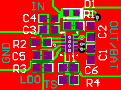
The bottom plane is a ground plane that is connected to the top through vias.
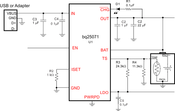 Figure 14. Schematic