SLUSBK6 July 2014
PRODUCTION DATA.
- 1 Features
- 2 Applications
- 3 Description
- 4 Application Schematic
- 5 Revision History
- 6 Device Comparison Table
- 7 Pin Configuration and Functions
- 8 Specifications
- 9 Detailed Description
- 10Application and Implementation
- 11Power Supply Recommendations
- 12Layout
- 13Device and Documentation Support
- 14Mechanical, Packaging, and Orderable Information
Package Options
Mechanical Data (Package|Pins)
- DQC|10
Thermal pad, mechanical data (Package|Pins)
Orderable Information
8 Specifications
8.1 Absolute Maximum Ratings(1)
over operating free-air temperature range (unless otherwise noted)| MIN | MAX | UNIT | ||
|---|---|---|---|---|
| Input Voltage | IN (with respect to GND) | –0.3 | 30 | V |
| EN, TS (with respect to GND) | –0.3 | 7 | V | |
| Output Voltage | BAT, OUT, LDO, CHG, ISET (with respect to GND) | –0.3 | 7 | V |
| Input Current (Continuous) | IN | 1.2 | A | |
| Output Current (Continuous) | BAT | 1.2 | A | |
| Output Current (Continuous) | LDO | 100 | mA | |
| Output Sink Current | CHG | 5 | mA | |
| Junction temperature, TJ | –40 | 150 | °C | |
(1) Stresses beyond those listed under absolute maximum ratings may cause permanent damage to the device. These are stress ratings only, and functional operation of the device at these or any other conditions beyond those indicated under recommended operating conditions is not implied. Exposure to absolute-maximum-rated conditions for extended periods may affect device reliability. All voltage values are with respect to the network ground pin unless otherwise noted.
8.2 Handling Ratings
| MIN | MAX | UNIT | |||
|---|---|---|---|---|---|
| TSTG | Storage temperature | –65 | 150 | °C | |
| VESD | Electrostatic discharge | Human body model (HBM), per ANSI/ESDA/JEDEC JS-001, all pins (1) | 0 | 3000 | V |
| Charged device model (CDM), per JEDEC specification JESD22-C101, all pins (2) | 0 | 1000 | V | ||
(1) JEDEC document JEP155 states that 500-V HBM allows safe manufacturing with a standard ESD control process.
(2) JEDEC document JEP157 states that 250-V CDM allows safe manufacturing with a standard ESD control process.
8.3 Recommended Operating Conditions
| MIN | MAX | UNITS | ||
|---|---|---|---|---|
| VIN | IN voltage | 3.75(1) | 28 | V |
| IN operating voltage | 3.75(1) | 10.2 | ||
| IIN | Input current, IN | 1 | A | |
| IOUT | Output Current in charge mode, OUT | 1 | A | |
| TJ | Junction Temperature | 0 | 125 | °C |
(1) Charge current may be limited at low input voltages due to the dropout of the device.
8.4 Thermal Information
| THERMAL METRIC(1) | bq25071 | UNIT | |
|---|---|---|---|
| DQC (10 PINS) | |||
| RθJA | Junction-to-ambient thermal resistance | 61.6 | °C/W |
| RθJC(top) | Junction-to-case (top) thermal resistance | 65.5 | |
| RθJB | Junction-to-board thermal resistance | 22.8 | |
| ψJT | Junction-to-top characterization parameter | 1.5 | |
| ψJB | Junction-to-board characterization parameter | 22.7 | |
| RθJC(bot) | Junction-to-case (bottom) thermal resistance | 5.5 | |
(1) For more information about traditional and new thermal metrics, see the IC Package Thermal Metrics application report, SPRA953.
8.5 Electrical Characteristics
Over junction temperature range 0°C ≤ TJ ≤ 125°C and recommended supply voltage (unless otherwise noted)| PARAMETER | TEST CONDITIONS | MIN | TYP | MAX | UNITS | |
|---|---|---|---|---|---|---|
| INPUT | ||||||
| V(UVLO) | Under-voltage lock-out | VIN: 0 V → 4 V | 3.15 | 3.30 | 3.55 | V |
| VHYS(UVLO) | Hysteresis on V(UVLO) | VIN: 4 V → 0 V | 250 | mV | ||
| VIN(SLP) | Valid input source threshold VIN(SLP) above VBAT | Input power good if VIN > VBAT + VIN(SLP)
V(BAT) = 3.6 V, VIN: 3.5 V → 4 V |
30 | 75 | 150 | mV |
| VHYS(INSLP) | Hysteresis on VIN(SLP) | V(BAT) = 3.6 V, VIN: 4 V → 3.5 V | 18 | 32 | 54 | mV |
| tDGL(NO-IN) | Delay time, input power loss to charger turn-off | Time measured from VIN: 5 V → 2.5 V 1 μs fall-time | 32 | ms | ||
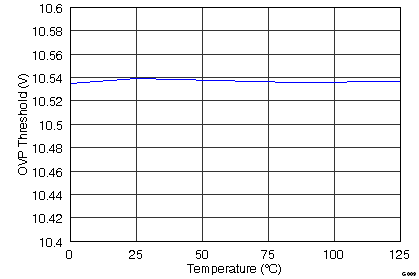
| VOVP | Input over-voltage protection threshold | VIN: 5 V → 11 V | 10.2 | 10.5 | 10.8 | V |
| VHYS(OVP) | Hysteresis on OVP | VIN: 11 V → 5 V | 100 | mV | ||
| QUIESCENT CURRENT | ||||||
| IBAT(PDWN) | Battery current into BAT, No input connected | VIN = 0 V(1), V(CHG) = Low, TJ = 85°C | 6 | μA | ||
| IIN(STDBY) | Standby current into IN pin | EN = HI, VIN = 5.5V | 0.25 | mA | ||
| EN = HI, VIN ≤ V(OVP) | 0.5 | |||||
| EN = HI, VIN > V(OVP) | 2 | |||||
| BATTERY CHARGER FAST-CHARGE | ||||||
| VBAT(REG) | Battery charge regulation voltage | TA = 0°C to 125°C, IOUT = 50 mA | 3.455 | 3.5 | 3.545 | V |
| TA = 25°C | 3.455 | 3.5 | 3.539 | |||
| VBAT(OVCH) | Battery overcharge voltage threshold | 3.62 | 3.7 | 3.78 | V | |
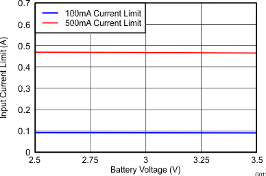
| IIN(RANGE) | User programmable input current limit range | R(ISET) = 1 kΩ to 1 0kΩ, EN = VSS | 100 | 1000 | mA | |
| IIN(LIM) | Input current limit, or fast-charge current | EN = FLOAT | 435 | 467 | 500 | mA |
| EN = VSS | KISET/RISET | |||||
| KISET | Fast charge current factor | R(ISET) = 1 kΩ to 10 kΩ, EN = VSS | 900 | 1000 | 1100 | AΩ |
| VDO(IN-OUT) | VIN – VOUT | VIN = 3.55 V, IOUT = 0.75 A | 500 | 900 | mV | |
| ISET SHORT CIRCUIT PROTECTION | ||||||
| RISET(MAX) | Highest resistor value considered a short fault | R(ISET): 900 Ω → 300 Ω, IOUT latches off, Cycle power to reset, Fault range > 1.10 A | 430 | 700 | Ω | |
| IOUT(CL) | Maximum OUT current limit regulation (Clamp) | 1.07 | 2 | A | ||
| PRE-CHARGE AND CHARGE DONE | ||||||
| V(LOWV) | Pre-charge to fast-charge transition threshold | 0.5 | 0.7 | 0.9 | V | |
| I(PRECHARGE) | Precharge current to BAT during precharge mode | V(BAT) = 0 V to 0.7 V | 41.5 | 45 | 48.5 | mA |
| RECHARGE OR REFRESH | ||||||
| V(RCH) | Recharge detection threshold | V(BAT) falling | 3.1 | 3.3 | 3.5 | V |
| LDO | ||||||
| V(LDO) | LDO Output Voltage | VIN = 5 V to 10.5 V, I(LDO) = 0 mA to 50 mA |
4.7 | 4.9 | 5.1 | V |
| I(LDO) | Maximum LDO Output Current | 60 | mA | |||
| V(DO) | Dropout Voltage | VIN = 4.5V, I(LDO) = 50 mA | 200 | 350 | mV | |
| LOGIC LEVELS ON EN | ||||||
| VIL | Logic low input voltage | 0.4 | V | |||
| VIH | Logic high input voltage | 1.4 | V | |||
| V(FLT) | Logic FLOAT input voltage | 600 | 850 | 1100 | mV | |
| I(FLTlkg) | Maximum leakage sink or source current to keep in FLOAT | 1 | µA | |||
| IEN(DRIVE) | Minimal drive current from an external device for Low or High | 8 | µA | |||
| BATTERY-PACK NTC MONITOR (TS) | ||||||
| V(COLD) | TS Cold Threshold | V(TS) Rising | 24.5 | 25 | 25.5 | %VLDO |
| V(CUTOFF) | TS Cold Cutoff Threshold | V(TS) Falling | 1 | %VLDO | ||
| V(HOT) | TS Hot Threshold | V(TS) Falling | 12 | 12.5 | 13 | %VLDO |
| VHOT(HYS) | TS Hot Cutoff Threshold | V(TS) Rising | 1 | %VLDO | ||
| CHG OUTPUT | ||||||
| VOL | Output LOW voltage | I(SINK) = 1 mA | 0.45 | V | ||
| IIH | Leakage current | CHG = 5 V | 1 | μA | ||
| THERMAL REGULATION | ||||||
| TJ(REG) | Temperature Regulation Limit | TJ rising | 125 | °C | ||
| TJ(OFF) | Thermal shutdown temperature | TJ rising | 155 | °C | ||
| TJ(OFF-HYS) | Thermal shutdown hysteresis | TJ falling | 20 | °C | ||
(1) Force V(CHG)
8.6 Timing Requirements
| MIN | TYP | MAX | UNIT | |||
|---|---|---|---|---|---|---|
| INPUT | ||||||
| tBLK(OVP) | Input overvoltage blanking time | 100 | μs | |||
| tREC(OVP) | Input overvoltage recovery time | Time measured from VIN: 11 V → 5 V 1 μs fall-time to LDO = HI, V(BAT) = 3.5 V |
100 | μs | ||
| ISET SHORT CIRCUIT PROTECTION | ||||||
| tDGL(SHORT) | Deglitch time transition from I(SET) short to IOUT disable | Clear fault by cycling V(BUS) or EN | 1.5 | ms | ||
| PRE-CHARGE AND CHARGE DONE | ||||||
| tDGL1(LOWV) | Deglitch time on pre-charge to fast-charge transition | 25 | ms | |||
| tDGL2(LOWV) | Deglitch time on fast-charge to pre-charge transition | 25 | ms | |||
| RECHARGE OR REFRESH | ||||||
| tDGL(RCH) | Deglitch time, recharge threshold detected | V(BAT) falling to New Charge Cycle | 25 | ms | ||
| BATTERY-PACK NTC MONITOR (TS) | ||||||
| tdgl(TS) | Deglitch for TS Fault | Fault detected on TS to stop charge | 25 | ms | ||
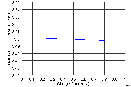
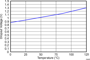
8.7 Typical Characteristics
VIN = 5 V, VBAT = 3.2 V, I(CHG) = 280 mA, Typical Application Circuit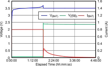
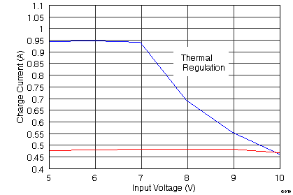
| VIN = 4.5 V | IOUT = 1 A | |
| VIN = 5 V | ||