SLUSBV8C August 2014 – November 2014
UNLESS OTHERWISE NOTED, this document contains PRODUCTION DATA.
- 1 Features
- 2 Applications
- 3 Description
- 4 Revision History
- 5 Device Comparison Table
- 6 Pin Configuration and Functions
- 7 Specifications
-
8 Detailed Description
- 8.1 Overview
- 8.2 Functional Block Diagram
- 8.3
Feature Description
- 8.3.1 Overvoltage-Protection (OVP) - Continuously Monitored
- 8.3.2 CHG Pin Indication (bq25101, bq25101H)
- 8.3.3 CHG Pin LED Pull-up Source (bq25101, bq25101H)
- 8.3.4 IN-DPM (VIN-DPM or IN-DPM)
- 8.3.5 OUT
- 8.3.6 ISET
- 8.3.7 PRE_TERM - Pre-Charge and Termination Programmable Threshold
- 8.3.8 TS
- 8.3.9 Timers
- 8.3.10 Termination
- 8.4 Device Functional Modes
- 9 Application and Implementation
- 10Power Supply Recommendations
- 11Layout
- 12Device and Documentation Support
- 13Mechanical, Packaging, and Orderable Information
Package Options
Mechanical Data (Package|Pins)
- YFP|6
Thermal pad, mechanical data (Package|Pins)
Orderable Information
11 Layout
11.1 Layout Guidelines
To obtain optimal performance, the decoupling capacitor from IN to GND and the output filter capacitors from OUT to GND should be placed as close as possible to the bq2510x, with short trace runs to both IN, OUT and GND.
- All low-current GND connections should be kept separate from the high-current charge or discharge paths from the battery. Use a single-point ground technique incorporating both the small signal ground path and the power ground path.
- The high current charge paths into IN pin and from the OUT pin must be sized appropriately for the maximum charge current in order to avoid voltage drops in these traces
11.2 Layout Example
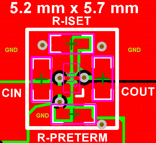 Figure 26. Board Layout
11.3 Thermal Package
The most common measure of package thermal performance is thermal impedance (θJA ) measured (or modeled) from the chip junction to the air surrounding the package surface (ambient). The mathematical expression for θJA is:
Where:
TJ = chip junction temperature
T = ambient temperature
P = device power dissipation
Factors that can influence the measurement and calculation of θJA include:
- Whether or not the device is board mounted
- Trace size, composition, thickness, and geometry
- Orientation of the device (horizontal or vertical)
- Volume of the ambient air surrounding the device under test and airflow
- Whether other surfaces are in close proximity to the device being tested
Due to the charge profile of Li-Ion and Li-Pol batteries the maximum power dissipation is typically seen at the beginning of the charge cycle when the battery voltage is at its lowest. Typically after fast charge begins the pack voltage increases to ≉3.4 V within the first 2 minutes. The thermal time constant of the assembly typically takes a few minutes to heat up so when doing maximum power dissipation calculations, 3.4 V is a good minimum voltage to use.
The device power dissipation, P, is a function of the charge rate and the voltage drop across the internal PowerFET. It can be calculated from the following equation when a battery pack is being charged :
The thermal loop feature reduces the charge current to limit excessive IC junction temperature. It is recommended that the design not run in thermal regulation for typical operating conditions (nominal input voltage and nominal ambient temperatures) and use the feature for non typical situations such as hot environments or higher than normal input source voltage. With that said, the IC will still perform as described, if the thermal loop is always active.