SLUSBV8C August 2014 – November 2014
UNLESS OTHERWISE NOTED, this document contains PRODUCTION DATA.
- 1 Features
- 2 Applications
- 3 Description
- 4 Revision History
- 5 Device Comparison Table
- 6 Pin Configuration and Functions
- 7 Specifications
-
8 Detailed Description
- 8.1 Overview
- 8.2 Functional Block Diagram
- 8.3
Feature Description
- 8.3.1 Overvoltage-Protection (OVP) - Continuously Monitored
- 8.3.2 CHG Pin Indication (bq25101, bq25101H)
- 8.3.3 CHG Pin LED Pull-up Source (bq25101, bq25101H)
- 8.3.4 IN-DPM (VIN-DPM or IN-DPM)
- 8.3.5 OUT
- 8.3.6 ISET
- 8.3.7 PRE_TERM - Pre-Charge and Termination Programmable Threshold
- 8.3.8 TS
- 8.3.9 Timers
- 8.3.10 Termination
- 8.4 Device Functional Modes
- 9 Application and Implementation
- 10Power Supply Recommendations
- 11Layout
- 12Device and Documentation Support
- 13Mechanical, Packaging, and Orderable Information
Package Options
Mechanical Data (Package|Pins)
- YFP|6
Thermal pad, mechanical data (Package|Pins)
Orderable Information
7 Specifications
7.1 Absolute Maximum Ratings(1)
over operating free-air temperature range (unless otherwise noted)| MIN | MAX | UNIT | ||||
|---|---|---|---|---|---|---|
| Input voltage | IN (with respect to VSS) | –0.3 | 30 | V | ||
| OUT (with respect to VSS) | –0.3 | 7 | V | |||
| PRE-TERM, ISET, TS, CHG
(with respect to VSS) |
–0.3 | 7 | V | |||
| Input current | IN | 300 | mA | |||
| Output current (continuous) | OUT | 300 | mA | |||
| Output sink current | CHG | 15 | mA | |||
| TJ | Junction temperature | –40 | 150 | °C | ||
(1) Stresses beyond those listed under absolute maximum ratings may cause permanent damage to the device. These are stress ratings only, and functional operation of the device at these or any other conditions beyond those indicated under recommended operating conditions is not implied. Exposure to absolute-maximum-rated conditions for extended periods may affect device reliability. All voltage values are with respect to the network ground terminal unless otherwise noted.
7.2 Handling Ratings
| MIN | MAX | UNIT | ||||
|---|---|---|---|---|---|---|
| ESD | Electrostatic discharge (IEC61000-4-2)(1) | IN, OUT, TS | 1 µF between IN and GND, 1 µF between TS and GND, 2 µF between OUT and GND, x5R Ceramic or equivalent |
8 contact 15 Air |
kV | |
| TSTG | Storage temperature | –65 | 150 | °C | ||
(1) The test was performed on IC pins that may potentially be exposed to the customer at the product level. The bq2510x IC requires a minimum of the listed capacitance, external to the IC, to pass the ESD test.
7.3 Recommended Operating Conditions (1)
| MIN | NOM | UNIT | ||
|---|---|---|---|---|
| VIN | IN voltage range | 3.5 | 28 | V |
| IN operating voltage range, Restricted by VDPM and VOVP | 4.45 | 6.45 | V | |
| IIN | Input current, IN pin | 250 | mA | |
| IOUT | Current, OUT pin | 250 | mA | |
| TJ | Junction temperature | 0 | 125 | °C |
| RPRE-TERM | Programs precharge and termination current thresholds | 0.6 | 30 | kΩ |
| RISET | Fast-charge current programming resistor | 0.54 | 13.5 | kΩ |
| RTS | 10k NTC thermistor range without entering BAT_EN or TTDM | 1.66 | 258 | kΩ |
(1) Operation with VIN less than 4.5V or in drop-out may result in reduced performance.
7.4 Thermal Information
| THERMAL METRIC(1) | bq25100 | UNIT | |
|---|---|---|---|
| YFP (6 PINS) | |||
| RθJA | Junction-to-ambient thermal resistance | 132.9 | °C/W |
| RθJCtop | Junction-to-case (top) thermal resistance | 1.3 | |
| RθJB | Junction-to-board thermal resistance | 21.8 | |
| ψJT | Junction-to-top characterization parameter | 5.6 | |
| ψJB | Junction-to-board characterization parameter | 21.8 | |
| RθJCbot | Junction-to-case (bottom) thermal resistance | n/a | |
(1) For more information about traditional and new thermal metrics, see the IC Package Thermal Metrics application report, SPRA953.
7.5 Electrical Characteristics
Over junction temperature range 0°C ≤ TJ ≤ 125°C and recommended supply voltage (unless otherwise noted)| PARAMETER | TEST CONDITIONS | MIN | TYP | MAX | UNIT | |
|---|---|---|---|---|---|---|
| INPUT | ||||||
| UVLO | Undervoltage lock-out exit | VIN: 0 V → 4 V | 3.15 | 3.3 | 3.45 | V |
| VHYS_UVLO | Hysteresis on VUVLO_RISE falling | VIN: 4 V→0 V; VUVLO_FALL = VUVLO_RISE – VHYS-UVLO |
250 | mV | ||
| VIN-DT | Input power good detection threshold is VOUT + VIN-DT | Input power good if VIN > VOUT + VIN-DT; VOUT = 3.6 V; VIN: 3.5 V → 4 V |
15 | 60 | 130 | mV |
| VHYS-INDT | Hysteresis on VIN-DT falling | VOUT = 3.6 V; VIN: 4 V → 3.5 V | 31 | mV | ||
| tDGL(PG_PWR) | Deglitch time on exiting sleep | Time measured from VIN: 0 V → 5 V 1-μs rise-time to charge enables; VOUT = 3.6 V | 29 | ms | ||
| tDGL(PG_NO-PWR) | Deglitch time on VHYS-INDT power down. Same as entering sleep. | Time measured from VIN: 5 V → 3.2 V 1-μs fall-time to charge disables; VOUT = 3.6 V | 29 | ms | ||
| VOVP | Input over-voltage protection threshold | VIN: 5 V → 12 V | 6.52 | 6.67 | 6.82 | V |
| tDGL(OVP-SET) | Input over-voltage blanking time | VIN: 5 V → 12 V | 113 | μs | ||
| VHYS-OVP | Hysteresis on OVP | VIN: 11 V → 5 V | 110 | mV | ||
| tDGL(OVP-REC) | Deglitch time exiting OVP | Time measured from VIN: 12 V → 5 V 1-μs fall-time to charge enables | 450 | μs | ||
| VIN-DPM | Low input voltage protection. Restricts lout at VIN-DPM | Limit input source current to 50 mA; VOUT = 3.5 V; RISET = 1.35 kΩ |
4.25 | 4.31 | 4.37 | V |
| ISET SHORT CIRCUIT TEST | ||||||
| RISET_SHORT | Highest resistor value considered a fault (short). | RISET: 540 Ω → 250 Ω, Iout latches off; Cycle power to reset |
420 | 450 | Ω | |
| tDGL_SHORT | Deglitch time transition from ISET short to Iout disable | Clear fault by disconnecting IN or cycling (high / low) TS/BAT_EN | 1 | ms | ||
| IOUT_CL | Maximum OUT current limit regulation (Clamp) | VIN = 5 V; VOUT = 3.6 V; RISET: 540 Ω → 250 Ω; IOUT latches off after tDGL-SHORT | 550 | 600 | 650 | mA |
| BATTERY SHORT PROTECTION | ||||||
| VOUT(SC) | OUT pin short-circuit detection threshold/ precharge threshold | VOUT:3 V → 0.5 V; No deglitch | 0.75 | 0.8 | 0.85 | V |
| VOUT(SC-HYS) | OUT pin Short hysteresis | Recovery ≥ VOUT(SC) + VOUT(SC-HYS); Rising; No deglitch | 77 | mV | ||
| IOUT(SC) | Source current to OUT pin during short-circuit detection | 9 | 11 | 13 | mA | |
| QUIESCENT CURRENT | ||||||
| IOUT(PDWN) | Battery current into OUT pin | VIN = 0 V; 0°C to 125°C | 75 | nA | ||
| VIN = 0 V; 0°C to 85°C | 50 | |||||
| IOUT(DONE) | OUT pin current, charging terminated | VIN = 6 V; VOUT > VOUT(REG) | 6 | μA | ||
| IIN(STDBY) | Standby current into IN pin | TS = GND; VIN ≤ 6 V | 125 | μA | ||
| ICC | Active supply current, IN pin | TS = open, VIN = 6 V; TTDM – no load on OUT pin; VOUT > VOUT(REG); IC enabled |
0.75 | 1 | mA | |
| BATTERY CHARGER FAST-CHARGE | ||||||
| VOUT(REG) | Output voltage | TJ = 0°C to 125°C; IOUT = 0 mA to 250 mA; VIN = 5.0 V; VTS-45°C≤ VTS ≤ VTS-0°C (bq25100/101) |
4.16 | 4.2 | 4.23 | V |
| TJ = 0°C to 125°C; IOUT = 0 mA to 250 mA; VIN = 5.0 V; VTS-45°C≤ VTS ≤ VTS-0°C (bq25100A) |
4.26 | 4.3 | 4.33 | |||
| TJ = 0°C to 125°C; IOUT = 0 mA to 250 mA; VIN = 5.0 V; VTS-45°C≤ VTS ≤ VTS-0°C (bq25100H/101H) |
4.31 | 4.35 | 4.38 | |||
| TJ = -5°C to 55°C; IOUT = 10mA to 75 mA; VIN = 5.0 V; VTS-45°C≤ VTS ≤ VTS-0°C (bq25100A) |
4.275 | 4.3 | 4.325 | |||
| VO_HT(REG) | Battery hot regulation voltage | VIN = 5.0 V; IOUT =10 mA to 250 mA; VTS-60°C≤ VTS ≤ VTS-45°C (bq25100/101) |
4.02 | 4.06 | 4.1 | V |
| VIN = 5.0 V; IOUT =10 mA to 250 mA; VTS-60°C≤ VTS ≤ VTS-45°C (bq25100H/101H) |
4.16 | 4.2 | 4.24 | |||
| IOUT(RANGE) | Programmed output “fast charge” current range | VOUT(REG) > VOUT > VLOWV; VIN = 5 V; RISET = 0.54 kΩ to 13.5 kΩ |
10 | 250 | mA | |
| VDO(IN-OUT) | Drop-Out, VIN – VOUT | Adjust VIN down until IOUT = 0.2 A; VOUT = 4.15 V; RISET = 680 Ω; TJ ≤ 100°C | 220 | 400 | mV | |
| IOUT | Output “fast charge” formula | VOUT(REG) > VOUT > VLOWV; VIN = 5 V | KISET/RISET | A | ||
| KISET | Fast charge current factor | RISET = KISET /IOUT; 20 < IOUT < 250 mA | 129 | 135 | 145 | AΩ |
| RISET = KISET /IOUT; 5 < IOUT < 20 mA | 125 | 135 | 145 | |||
| PRECHARGE – SET BY PRETERM PIN | ||||||
| VLOWV | Pre-charge to fast-charge transition threshold | 2.4 | 2.5 | 2.6 | V | |
| tDGL1(LOWV) | Deglitch time on pre-charge to fast-charge transition | 57 | μs | |||
| tDGL2(LOWV) | Deglitch time on fast-charge to pre-charge transition | 32 | ms | |||
| IPRE-TERM | Refer to the Termination Section | |||||
| %PRECHG | Pre-charge current, default setting | VOUT < VLOWV; RISET = 2.7 kΩ; RPRE-TERM= High Z or for BQ25101/101H | 18 | 20 | 22 | %IOUT-CC |
| Pre-charge current formula | RPRE-TERM = KPRE-CHG (Ω/%) × %PRE-CHG (%) | RPRE-TERM/KPRE-CHG% | ||||
| KPRE-CHG | % Pre-charge Factor | VOUT < VLOWV; VIN = 5 V; RPRE-TERM = 6 kΩ to 30 kΩ; RISET = 1.8 kΩ; RPRE-TERM = KPRE-CHG × %IPRE-CHG, where %IPRE-CHG is 20 to 100% |
280 | 300 | 320 | Ω/% |
| VOUT < VLOWV; VIN = 5 V; RPRE-TERM = 3 kΩ to 6 kΩ; RISET = 1.8 kΩ; RPRE-TERM = KPRE-CHG × %IPRE-CHG, where %IPRE-CHG is 10% to 20% |
265 | 300 | 340 | Ω/% | ||
| TERMINATION – SET BY PRE-TERM PIN | ||||||
| %TERM | Termination threshold current, default setting | VOUT > VRCH; RISET = 2.7 kΩ; RPRE-TERM = High Z or for BQ25101/101H | 9 | 10 | 11 | %IOUT-CC |
| Termination current threshold formula | RPRE-TERM = KTERM (Ω/%) × %TERM (%) | RPRE-TERM/ KTERM | ||||
| KTERM | % Term factor | VOUT > VRCH; VIN = 5 V; RPRE-TERM = 6 kΩ to 30 kΩ; RISET = 1.8 kΩ, RPRE-TERM=KTERM × %ITERM, where %ITERM is 10 to 50% |
575 | 600 | 640 | Ω/% |
| VOUT > VRCH; VIN = 5 V; RPRE-TERM = 3 kΩ to 6 kΩ ; RISET = 1.8 kΩ, RPRE-TERM= KTERM × %ITERM, where %ITERM is 5 to 10% |
555 | 620 | 685 | |||
| VOUT > VRCH; VIN = 5 V; RPRE-TERM = 750 Ω to 3 kΩ; RISET = 1.8 kΩ, RPRE-TERM= KTERM × %ITERM, where %ITERM is 1.25% to 5% |
352 | 680 | 1001 | |||
| IPRE-TERM | Current for programming the term. and pre-chg with resistor, ITerm-Start is the initial PRE-TERM current | RPRE-TERM = 6 kΩ; VOUT = 4.15 V | 23 | 25 | 27 | μA |
| ITERM | Termination current range | Minimum absolute termination current | 1 | mA | ||
| %TERM | Termination current formula | RTERM/ KTERM | % | |||
| tDGL(TERM) | Deglitch time, termination detected | 29 | ms | |||
| RECHARGE OR REFRESH | ||||||
| VRCH | Recharge detection threshold – normal temp | VIN = 5 V; VTS = 0.5 V; VOUT: 4.25 V → VRCH (bq25100); VOUT: 4.35 V → VRCH (bq25100A); VOUT: 4.40 V → VRCH (bq25100H) |
VO(REG)
–0.125 |
VO(REG)–0.095 | VO(REG)–0.075 | V |
| Recharge detection threshold – hot temp | VIN = 5 V; VTS = 0.2 V; VOUT: 4.15 V → VRCH (bq25100); VOUT: 4.25 V → VRCH (bq25100H) |
VO_HT(REG)
–0.130 |
VO_HT(REG)
–0.105 |
VO_HT(REG)
–0.080 |
V | |
| tDGL1(RCH) | Deglitch time, recharge threshold detected | VIN = 5 V; VTS = 0.5 V; VOUT: 4.25 V → 3.5V in 1 μs; tDGL(RCH) is time to ISET ramp |
29 | ms | ||
| tDGL2(RCH) | Deglitch time, recharge threshold detected in OUT-Detect Mode | VIN = 5 V; VTS = 0.5 V; VOUT = 3.5 V inserted; tDGL(RCH) is time to ISET ramp |
29 | ms | ||
| BATTERY DETECT ROUTINE – (NOTE: In Hot mode VO(REG) becomes VO_HT(REG)) | ||||||
| VREG-BD | VOUT reduced regulation during battery detect | bq25100/101/bq25100H/101H; VIN = 5 V; VTS = 0.5 V, Battery absent |
VO(REG)-0.450 | VO(REG)-0.400 | VO(REG)-0.350 | V |
| bq25100A; VIN = 5 V; VTS = 0.5 V; Battery absent |
VO(REG)-0.550 | VO(REG)-0.500 | VO(REG)-0.450 | |||
| IBD-SINK | Sink current during VREG-BD | VIN = 5 V; VTS = 0.5 V; Battery absent | 2 | mA | ||
| tDGL(HI/LOW REG) | Regulation time at VREG or VREG-BD | VIN = 5 V; VTS = 0.5 V; Battery absent | 25 | ms | ||
| VBD-HI | High battery detection threshold | VIN = 5 V; VTS = 0.5 V; Battery absent | VO(REG) -0.150 | VO(REG)-0.100 | VO(REG)-0.050 | V |
| VBD-LO | Low battery detection threshold | VIN = 5 V; VTS = 0.5 V; Battery absent | VREG-BD
+0.05 |
VREG-BD +0.1 | VREG-BD
+0.15 |
V |
| BATTERY CHARGING TIMERS AND FAULT TIMERS | ||||||
| tPRECHG | Pre-charge safety timer value | Restarts when entering pre-charge; Always enabled when in pre-charge. |
1700 | 1940 | 2250 | s |
| tMAXCH | Charge safety timer value | Clears fault or resets at UVLO, TS disable, OUT Short, exiting LOWV and Refresh | 34000 | 38800 | 45000 | s |
| BATTERY-PACK NTC MONITOR (see Note 1); TS pin: 10k NTC | ||||||
| INTC-10k | NTC bias current | VTS = 0.3 V | 48.5 | 50.5 | 52.5 | μA |
| INTC-DIS-10k | 10k NTC bias current when charging is disabled | VTS = 0 V | 27 | 30 | 33 | μA |
| INTC-FLDBK-10k | INTC is reduced prior to entering TTDM to keep cold thermistor from entering TTDM | VTS: Set to 1.525 V | 4 | 5 | 6.5 | μA |
| VTTDM(TS) | Termination and timer disable mode Threshold – Enter | VTS: 0.5 V → 1.7 V; Timer held in reset | 1550 | 1600 | 1650 | mV |
| VHYS-TTDM(TS) | Hysteresis exiting TTDM | VTS: 1.7 V → 0.5 V; Timer enabled | 100 | mV | ||
| VCLAMP(TS) | TS maximum voltage clamp | VTS = Open (float) | 1900 | 1950 | 2000 | mV |
| tDGL(TTDM) | Deglitch exit TTDM between states | 57 | ms | |||
| Deglitch enter TTDM between states | 8 | μs | ||||
| VTS_I-FLDBK | TS voltage where INTC is reduce to keep thermistor from entering TTDM | INTC adjustment (90 to 10%; 45 to 6.6 uA) takes place near this spec threshold; VTS: 1.425 V → 1.525 V |
1475 | mV | ||
| CTS | Optional capacitance – ESD | 0.22 | μF | |||
| VTS-0°C | Low temperature CHG pending | Low temp charging to pending; VTS: 1 V → 1.5 V |
1230 | 1255 | 1280 | mV |
| VHYS-0°C | Hysteresis | At 0°C; Charge pending to low temp charging; VTS: 1.5 V → 1 V |
100 | mV | ||
| VTS-10°C | Low temperature, half charge | Normal charging to low temp charging; VTS: 0.5 V → 1 V |
775 | 800 | 830 | mV |
| VHYS-10°C | Hysteresis | At 10°C; Low temp charging to normal CHG; VTS: 1 V → 0.5 V |
55 | mV | ||
| VTS-45°C | High temperature | At 4.1V (bq25100/101) or 4.2V (bq25100H/101H); Normal charging to high temp CHG; VTS: 0.5 V → 0.2 V |
253 | 268 | 283 | mV |
| VHYS-45°C | Hysteresis | At 45°C; High temp charging to normal CHG; VTS: 0.2 V → 0.5 V |
20 | mV | ||
| VTS-60°C | High temperature disable | bq25100/01/100H/101H/100L; High temp charge to pending; VTS: 0.2 V → 0.1 V |
160 | 170 | 180 | mV |
| VHYS-60°C | Hysteresis | At 60°C (bq25100/01/100H/101H/100L); Charge pending to high temp CHG; VTS: 0.1 V → 0.2 V |
20 | mV | ||
| tDGL(TS_10C) | Deglitch for TS thresholds: 10C | Normal to cold operation; VTS: 0.6 V → 1 V | 50 | ms | ||
| Cold to normal operation; VTS: 1 V → 0.6 V | 12 | |||||
| tDGL(TS) | Deglitch for TS thresholds: 0/45/60C | Battery charging | 30 | ms | ||
| VTS-EN-10k | Charge enable threshold, (10k NTC) | VTS: 0 V → 0.175 V | 84 | 92 | 100 | mV |
| VTS-DIS_HYS-10k | HYS below VTS-EN-10k to disable, (10k NTC) | VTS: 0.125 V → 0 V | 12 | mV | ||
| THERMAL REGULATION | ||||||
| TJ(REG) | Temperature regulation limit | 125 | °C | |||
| TJ(OFF) | Thermal shutdown temperature | 155 | °C | |||
| TJ(OFF-HYS) | Thermal shutdown hysteresis | 20 | °C | |||
| LOGIC LEVELS ON /CHG | ||||||
| VOL | Output low voltage | ISINK = 5 mA | 0.4 | V | ||
| ILEAK | Leakage current into IC | VCHG = 5 V | 1 | μA | ||
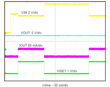
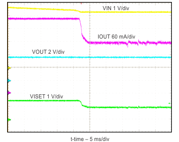
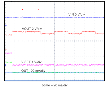
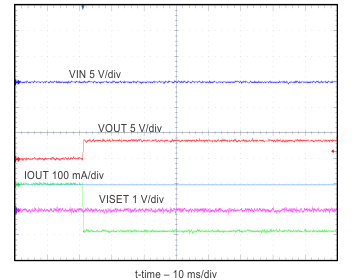
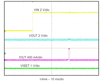
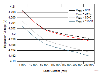
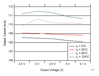
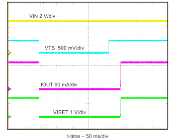
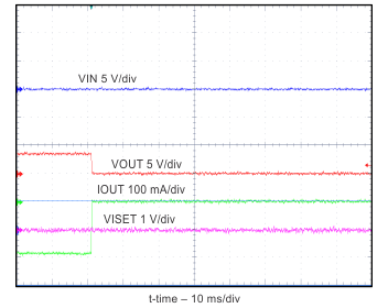
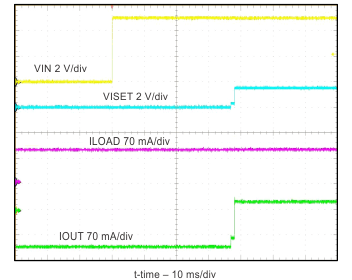
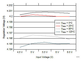
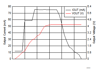
7.6 Typical Characteristics
Setup: Typical Applications Schematic; VIN = 5 V, VBAT = 3.6 V (unless otherwise noted)
| No Battery, No Load | ||
| VIN 0 V -5 V-7 V-5 V | ||
| VIN Regulated | ||
| No Load | ||
| 20-Ω resistor at OUT, No input, VBAT = 3.7 V | ||
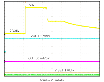
| Hot Plug | ||
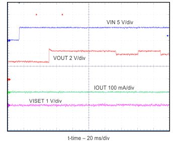
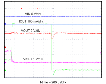
| 20-Ω resistor at OUT, No input, VBAT = 3.7 V | ||
| 90-mA Load, 120-mA ICHG | ||
| bq25100 charge cycle, ICHG = 75 mA, VBAT_REG = 4.2 V | ||