SLUSDJ8A April   2020  – April 2021 BQ25170

PRODUCTION DATA  

  1. Features
  2. Applications
  3. Description
  4. Revision History
  5. Pin Configuration and Functions
  6. Specifications
    1. 6.1 Absolute Maximum Ratings
    2. 6.2 ESD Ratings
    3. 6.3 Recommended Operating Conditions
    4. 6.4 Thermal Information
    5. 6.5 Electrical Characteristics
    6. 6.6 Timing Requirements
    7. 6.7 Typical Characteristics
  7. Detailed Description
    1. 7.1 Overview
    2. 7.2 Functional Block Diagram
    3. 7.3 Feature Description
      1. 7.3.1 Device Power Up from Input Source
        1. 7.3.1.1 ISET Pin Detection
        2. 7.3.1.2 VSET Pin Detection
        3. 7.3.1.3 Charger Power Up
      2. 7.3.2 Battery Charging Features
        1. 7.3.2.1 Lithium-Ion Battery Charging Profile
        2. 7.3.2.2 Charge Termination and Battery Recharge
        3. 7.3.2.3 Charging Safety Timers
        4. 7.3.2.4 Battery Cold, Hot Temperature Qualification (TS Pin)
      3. 7.3.3 Status Outputs ( PG, STAT)
        1. 7.3.3.1 Power Good Indicator (PG Pin)
        2. 7.3.3.2 Charging Status Indicator (STAT)
      4. 7.3.4 Protection Features
        1. 7.3.4.1 Input Overvoltage Protection (VIN OVP)
        2. 7.3.4.2 Output Overvoltage Protection (BAT OVP)
        3. 7.3.4.3 Output Overcurrent Protection (BAT OCP)
        4. 7.3.4.4 Thermal Regulation and Thermal Shutdown (TREG and TSHUT)
    4. 7.4 Device Functional Modes
      1. 7.4.1 Shutdown or Undervoltage Lockout (UVLO)
      2. 7.4.2 Sleep Mode
      3. 7.4.3 Active Mode
        1. 7.4.3.1 Standby Mode
      4. 7.4.4 Fault Mode
  8. Application and Implementation
    1. 8.1 Application Information
    2. 8.2 Typical Applications
      1. 8.2.1 Li-Ion Charger Design Example
        1. 8.2.1.1 Design Requirements
        2. 8.2.1.2 Detailed Design Procedure
          1. 8.2.1.2.1 TS Function
        3. 8.2.1.3 Application Curves
      2. 8.2.2 LiFePO4 Charger Design Example
        1. 8.2.2.1 Design Requirements
  9. Power Supply Recommendations
  10. 10Layout
    1. 10.1 Layout Guidelines
    2. 10.2 Layout Example
  11. 11Device and Documentation Support
    1. 11.1 Device Support
      1. 11.1.1 Third-Party Products Disclaimer
    2. 11.2 Receiving Notification of Documentation Updates
    3. 11.3 Support Resources
    4. 11.4 Trademarks
    5. 11.5 Electrostatic Discharge Caution
    6. 11.6 Glossary
  12. 12Mechanical, Packaging, and Orderable Information

Package Options

Mechanical Data (Package|Pins)
Thermal pad, mechanical data (Package|Pins)
Orderable Information

Application Curves

CIN = 1 µF, COUT = 1 µF, VIN = 5 V, VOUT = 3.8 V, ICHG = 250 mA (unless otherwise specified)
GUID-20210211-CA0I-TR6D-5HFR-QRFJ01J5MXLS-low.png
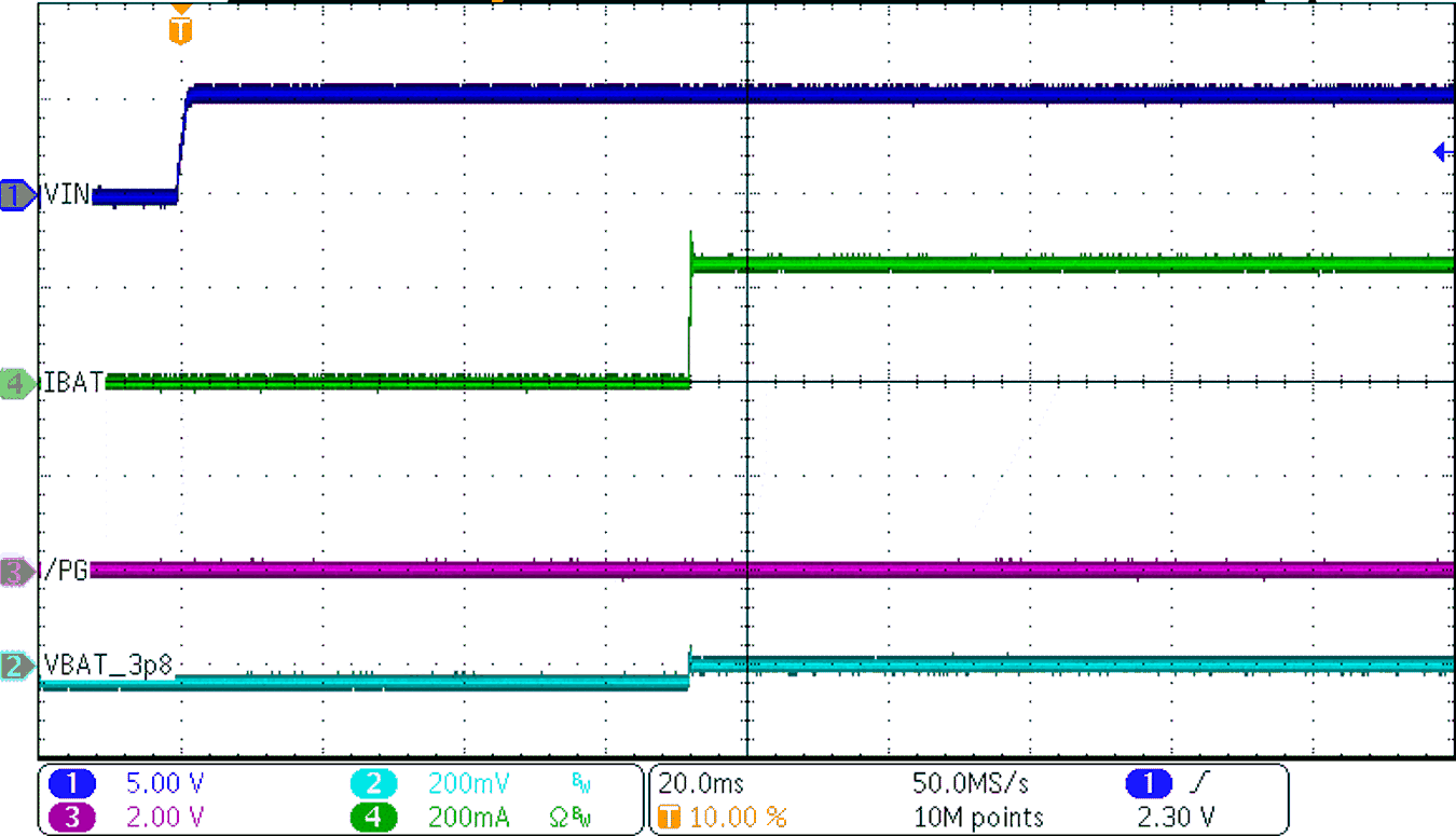
RISET = 1.2 kΩ
Figure 8-2 Power Up With Battery
GUID-20210211-CA0I-QDTH-L0RQ-ZNX90KM3JCKP-low.png
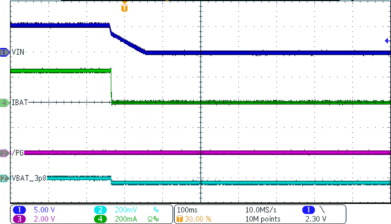
VIN = 5 V → 0 V
Figure 8-4 Power Down
GUID-20210211-CA0I-MTMN-1BFS-RZDR7Z3KL3TZ-low.png
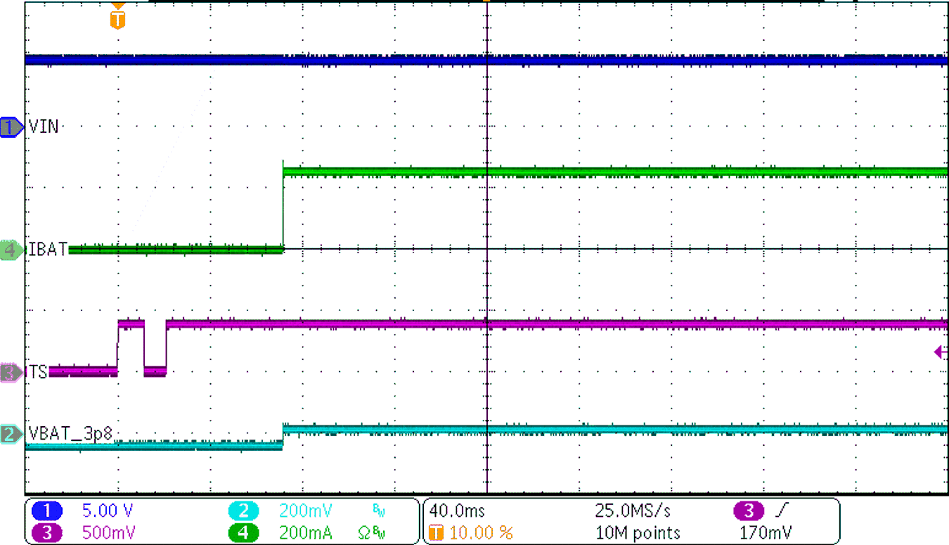
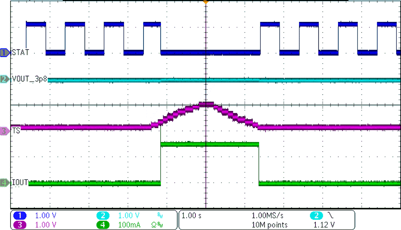
TS pin released
Figure 8-6 Charge Enable
GUID-20210211-CA0I-HZ1N-2ZKJ-WBWHLTTZB3X0-low.png
VIN = 4 V → 6 V VOUT = 3.5 V
Figure 8-8 IN Transient Response
GUID-20210211-CA0I-VFW5-QVWW-MHKCBJ6ZQNSZ-low.png
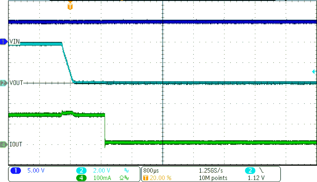
VOUT = 4.0 V → 0 V
Figure 8-10 OUT Short-Circuit Response
GUID-20210211-CA0I-PKSD-L87J-6RQ490R798RS-low.png
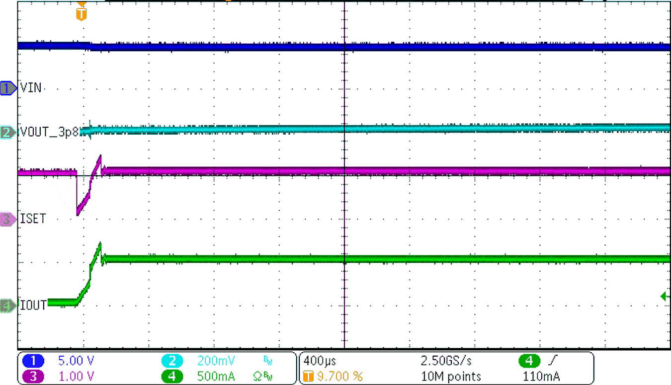
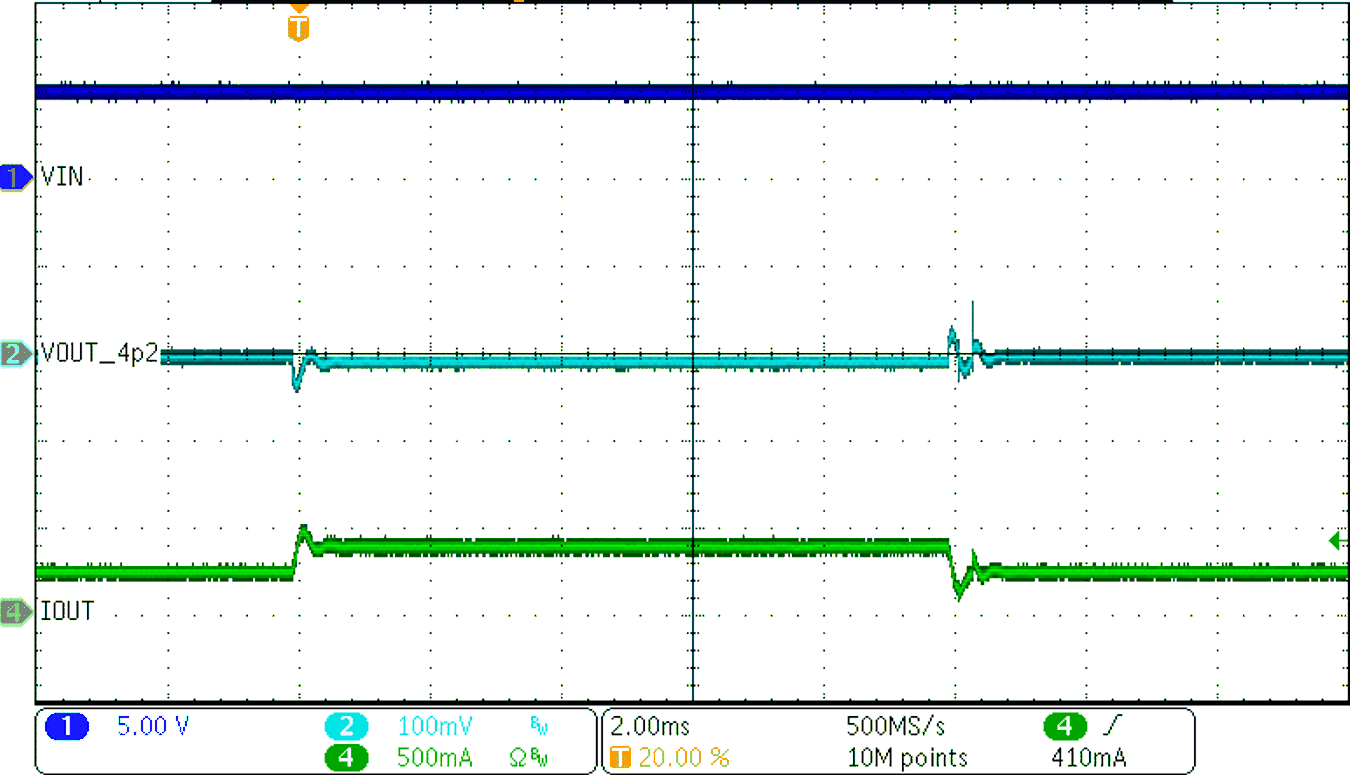
ISET = 50 mA → 500 mA
Figure 8-12 ISET Change Response
GUID-20210211-CA0I-2PJP-XLBK-8VD4LSPFFMPX-low.png
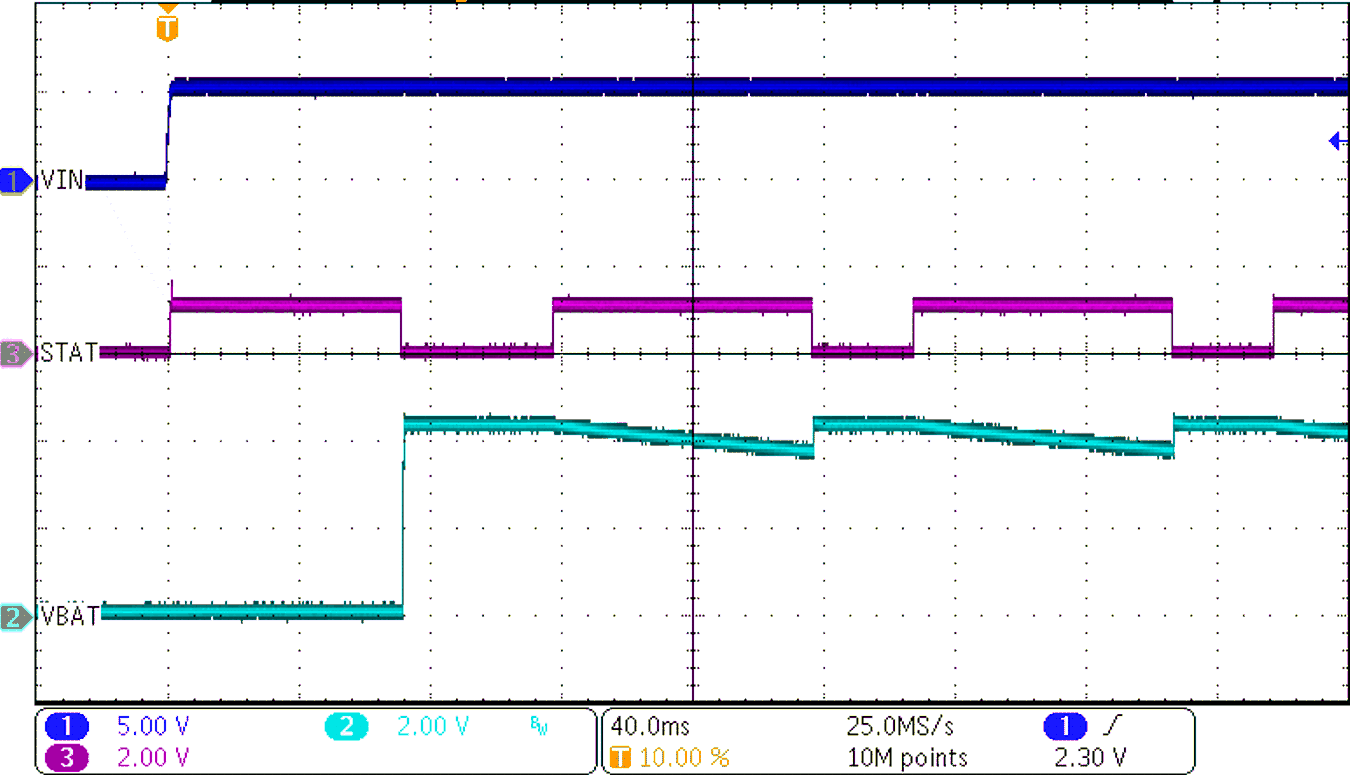
RISET = 1.2 kΩ OUT = open-circuit
Figure 8-3 Power Up Without Battery
GUID-20210211-CA0I-KXSD-TSV0-8PNRX6PMD7RL-low.png
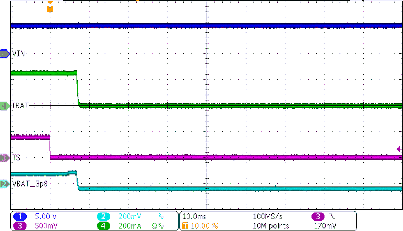
TS pulled LOW
Figure 8-5 Charge Disable
GUID-20210211-CA0I-LMBR-ZLHJ-MWBCHX8RX42F-low.png
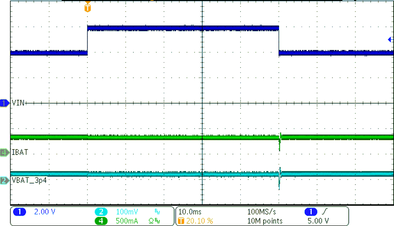
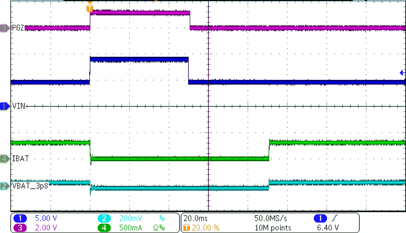
VIN = 5 V → 10 V → 5 V
Figure 8-7 IN OVP Response
GUID-20210211-CA0I-JS4M-LGXN-TJPRWMWK88FH-low.png
VOUT = VSET = 4.2 V ISYS = 0 mA → 500 mA
Figure 8-9 OUT Transient Response
GUID-20210211-CA0I-KB7Q-B62X-HSDP9GNT3KHZ-low.png
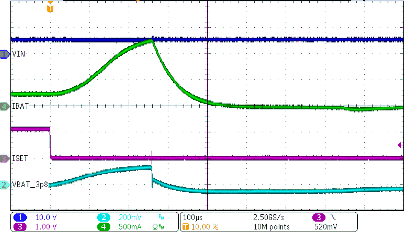
ISET = 1.2 kΩ → 0 Ω
Figure 8-11 ISET Short-Circuit Response
GUID-20210211-CA0I-ZLPT-ZWD0-RDXK28HTKZ66-low.png
VTS = 80 mV → 1 V → 80 mV
Figure 8-13 TS Change Response