SLUSF68 july   2023 BQ25173-Q1

PRODUCTION DATA  

  1.   1
  2. Features
  3. Applications
  4. Description
  5. Revision History
  6. Pin Configuration and Functions
  7. Specifications
    1. 6.1 Absolute Maximum Ratings
    2. 6.2 ESD Ratings
    3. 6.3 Recommended Operating Conditions
    4. 6.4 Thermal Information
    5. 6.5 Electrical Characteristics
    6. 6.6 Timing Requirements
    7. 6.7 Typical Characteristics
  8. Detailed Description
    1. 7.1 Overview
    2. 7.2 Functional Block Diagram
    3. 7.3 Feature Description
      1. 7.3.1 Device Power Up from Input Source
        1. 7.3.1.1 ISET Pin Detection
      2. 7.3.2 Supercapacitor Regulation Voltage
      3. 7.3.3 Supercapacitor Charging Profile
      4. 7.3.4 Status Outputs (PG, STAT)
        1. 7.3.4.1 Power Good Indicator (PG Pin)
        2. 7.3.4.2 Charging Status Indicator (STAT)
      5. 7.3.5 Protection Features
        1. 7.3.5.1 Input Overvoltage Protection (VIN OVP)
        2. 7.3.5.2 Output Overcurrent Protection (OUT OCP)
        3. 7.3.5.3 Thermal Regulation and Thermal Shutdown (TREG and TSHUT)
    4. 7.4 Device Functional Modes
      1. 7.4.1 Shutdown or Undervoltage Lockout (UVLO)
      2. 7.4.2 Sleep Mode
      3. 7.4.3 Active Mode
        1. 7.4.3.1 Standby Mode
      4. 7.4.4 Fault Mode
  9. Application and Implementation
    1. 8.1 Application Information
    2. 8.2 Typical Applications
      1. 8.2.1 1s Supercapacitor Charger Design Example
        1. 8.2.1.1 Design Requirements
        2. 8.2.1.2 Detailed Design Procedure
        3. 8.2.1.3 Application Curves
      2. 8.2.2 4s Supercapacitor Charger Design Example
        1. 8.2.2.1 Design Requirements
        2. 8.2.2.2 Application Curves
  10. Power Supply Recommendations
  11. 10Layout
    1. 10.1 Layout Guidelines
    2. 10.2 Layout Example
    3. 10.3 Thermal Considerations
  12. 11Device and Documentation Support
    1. 11.1 Device Support
      1. 11.1.1 Third-Party Products Disclaimer
    2. 11.2 Receiving Notification of Documentation Updates
    3. 11.3 Support Resources
    4. 11.4 Trademarks
    5. 11.5 Electrostatic Discharge Caution
    6. 11.6 Glossary
  13. 12Mechanical, Packaging, and Orderable Information

Package Options

Mechanical Data (Package|Pins)
Thermal pad, mechanical data (Package|Pins)
Orderable Information

ISET Pin Detection

After a valid VIN is plugged in and the CE pin is pulled LOW, the device checks the resistor on the ISET pin for a short circuit (RISET < RISET_SHORT). If a short condition is detected, the charger remains in the FAULT state until the input or CE pin is toggled. If the ISET pin is open circuit, the charger proceeds through pin detection and starts the charger with no charge current. This pin is monitored during charging and changes in RISET while the charger is operating immediately translates to changes in charge current.

An external pulldown resistor (±1% or better recommended to minimize charge current error) from the ISET pin to GND sets the charge current as:
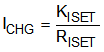
Equation 1. GUID-DDDA6D22-FF1A-4D1C-8042-8C8D50441874-low.gif

where:

  • ICHG is the desired fast-charge current
  • KISET is the gain factor found in the electrical specifications
  • RISET is the pulldown resistor from the ISET pin to GND

For charge currents below 50 mA, an extra RC circuit is recommended on the ISET pin to achieve a more stable current signal. For greater accuracy at lower currents, part of the current-sensing FET is disabled to give better resolution.