SLUSF68 july   2023 BQ25173-Q1

PRODUCTION DATA  

  1.   1
  2. Features
  3. Applications
  4. Description
  5. Revision History
  6. Pin Configuration and Functions
  7. Specifications
    1. 6.1 Absolute Maximum Ratings
    2. 6.2 ESD Ratings
    3. 6.3 Recommended Operating Conditions
    4. 6.4 Thermal Information
    5. 6.5 Electrical Characteristics
    6. 6.6 Timing Requirements
    7. 6.7 Typical Characteristics
  8. Detailed Description
    1. 7.1 Overview
    2. 7.2 Functional Block Diagram
    3. 7.3 Feature Description
      1. 7.3.1 Device Power Up from Input Source
        1. 7.3.1.1 ISET Pin Detection
      2. 7.3.2 Supercapacitor Regulation Voltage
      3. 7.3.3 Supercapacitor Charging Profile
      4. 7.3.4 Status Outputs (PG, STAT)
        1. 7.3.4.1 Power Good Indicator (PG Pin)
        2. 7.3.4.2 Charging Status Indicator (STAT)
      5. 7.3.5 Protection Features
        1. 7.3.5.1 Input Overvoltage Protection (VIN OVP)
        2. 7.3.5.2 Output Overcurrent Protection (OUT OCP)
        3. 7.3.5.3 Thermal Regulation and Thermal Shutdown (TREG and TSHUT)
    4. 7.4 Device Functional Modes
      1. 7.4.1 Shutdown or Undervoltage Lockout (UVLO)
      2. 7.4.2 Sleep Mode
      3. 7.4.3 Active Mode
        1. 7.4.3.1 Standby Mode
      4. 7.4.4 Fault Mode
  9. Application and Implementation
    1. 8.1 Application Information
    2. 8.2 Typical Applications
      1. 8.2.1 1s Supercapacitor Charger Design Example
        1. 8.2.1.1 Design Requirements
        2. 8.2.1.2 Detailed Design Procedure
        3. 8.2.1.3 Application Curves
      2. 8.2.2 4s Supercapacitor Charger Design Example
        1. 8.2.2.1 Design Requirements
        2. 8.2.2.2 Application Curves
  10. Power Supply Recommendations
  11. 10Layout
    1. 10.1 Layout Guidelines
    2. 10.2 Layout Example
    3. 10.3 Thermal Considerations
  12. 11Device and Documentation Support
    1. 11.1 Device Support
      1. 11.1.1 Third-Party Products Disclaimer
    2. 11.2 Receiving Notification of Documentation Updates
    3. 11.3 Support Resources
    4. 11.4 Trademarks
    5. 11.5 Electrostatic Discharge Caution
    6. 11.6 Glossary
  13. 12Mechanical, Packaging, and Orderable Information

Package Options

Mechanical Data (Package|Pins)
Thermal pad, mechanical data (Package|Pins)
Orderable Information

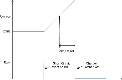
Output Overcurrent Protection (OUT OCP)

During normal operation, the OUT current should be regulated to the ISET programmed value. However, if a short circuit occurs on the ISET pin, the OUT current may rise to an unintended level. If current at the OUT pin exceeds IOUT_OCP, the device turns off after a deglitch, tOUT_OCP_DGL, and the device remains latched off. An input supply or CE pin toggle is required to restart operation.
GUID-F5602AF0-DE64-47BB-994D-24DD3C9CC5D0-low.gifFigure 7-3 Overcurrent Protection