SLUSDF7A January   2020  – February 2022 BQ25616

PRODUCTION DATA  

  1. Features
  2. Applications
  3. Description
  4. Revision History
  5. Description (continued)
  6. Device Comparison Table
  7. Pin Configuration and Functions
  8. Specifications
    1. 8.1 Absolute Maximum Ratings
    2. 8.2 ESD Ratings
    3. 8.3 Recommended Operating Conditions
    4. 8.4 Thermal Information
    5. 8.5 Electrical Characteristics
    6. 8.6 Timing Requirements
    7. 8.7 Typical Characteristics
  9. Detailed Description
    1. 9.1 Overview
    2. 9.2 Functional Block Diagram
    3. 9.3 Feature Description
      1. 9.3.1 Power-On-Reset (POR)
      2. 9.3.2 Device Power Up From Battery Without Input Source
      3. 9.3.3 Power Up From Input Source
        1. 9.3.3.1 Power Up ACFET
        2. 9.3.3.2 Power Up REGN LDO
        3. 9.3.3.3 Poor Source Qualification
        4. 9.3.3.4 Input Source Type Detection (IINDPM Threshold)
          1. 9.3.3.4.1 D+/D– Detection Sets Input Current Limit
        5. 9.3.3.5 Input Voltage Limit Threshold Setting (VINDPM Threshold)
        6. 9.3.3.6 Power Up Converter in Buck Mode
      4. 9.3.4 Boost Mode Operation From Battery
      5. 9.3.5 Standalone Charger
      6. 9.3.6 Power Path Management
        1. 9.3.6.1 Narrow VDC Architecture
        2. 9.3.6.2 Dynamic Power Management
        3. 9.3.6.3 Supplement Mode
      7. 9.3.7 Battery Charging Management
        1. 9.3.7.1 Autonomous Charging Cycle
        2. 9.3.7.2 Battery Charging Profile
        3. 9.3.7.3 Charging Termination
        4. 9.3.7.4 Thermistor Qualification
          1. 9.3.7.4.1 JEITA Guideline Compliance During Charging Mode (BQ25616J)
          2. 9.3.7.4.2 Hot/Cold Temperature Window During Charging Mode (BQ25616)
          3. 9.3.7.4.3 Boost Mode Thermistor Monitor During Battery Discharge Mode
        5. 9.3.7.5 Charging Safety Timer
      8. 9.3.8 Status Outputs ( PG, STAT)
        1. 9.3.8.1 Power Good Indicator ( PG Pin )
        2. 9.3.8.2 Charging Status Indicator (STAT)
      9. 9.3.9 Protections
        1. 9.3.9.1 Input Current Limit
        2. 9.3.9.2 Voltage and Current Monitoring in Buck Mode
          1. 9.3.9.2.1 Input Overvoltage Protection (ACOV)
          2. 9.3.9.2.2 System Overvoltage Protection (SYSOVP)
        3. 9.3.9.3 Voltage and Current Monitoring in Boost Mode
          1. 9.3.9.3.1 Boost Mode Overvoltage Protection
        4. 9.3.9.4 Thermal Regulation and Thermal Shutdown
          1. 9.3.9.4.1 Thermal Protection in Buck Mode
          2. 9.3.9.4.2 Thermal Protection in Boost Mode
        5. 9.3.9.5 Battery Protection
          1. 9.3.9.5.1 Battery Overvoltage Protection (BATOVP)
          2. 9.3.9.5.2 Battery Overdischarge Protection
          3. 9.3.9.5.3 System Overcurrent Protection
    4. 9.4 Device Functional Modes
  10. 10Application and Implementation
    1. 10.1 Application Information
    2. 10.2 Typical Applications
      1. 10.2.1 BQ25616/616J Application without External OVP
        1. 10.2.1.1 Design Requirements
        2. 10.2.1.2 Detailed Design Procedure
          1. 10.2.1.2.1 Inductor Selection
          2. 10.2.1.2.2 Input Capacitor and Resistor
          3. 10.2.1.2.3 Output Capacitor
        3. 10.2.1.3 Application Curves
      2. 10.2.2 BQ25616/616J Application with External OVP
        1. 10.2.2.1 Design Requirements
        2. 10.2.2.2 Detailed Design Procedure
        3. 10.2.2.3 Application Curves
  11. 11Power Supply Recommendations
  12. 12Layout
    1. 12.1 Layout Guidelines
    2. 12.2 Layout Example
  13. 13Device and Documentation Support
    1. 13.1 Device Support
      1. 13.1.1 Third-Party Products Disclaimer
    2. 13.2 Documentation Support
      1. 13.2.1 Related Documentation
    3. 13.3 Receiving Notification of Documentation Updates
    4. 13.4 Support Resources
    5. 13.5 Trademarks
    6. 13.6 Electrostatic Discharge Caution
    7. 13.7 Glossary
  14. 14Mechanical, Packaging, and Orderable Information

Package Options

Mechanical Data (Package|Pins)
Thermal pad, mechanical data (Package|Pins)
Orderable Information
JEITA Guideline Compliance During Charging Mode (BQ25616J)

To improve the safety of charging Li-ion batteries, the JEITA guideline was released on April 20, 2007. The guideline emphasized the importance of avoiding a high charge current and high charge voltage at certain low and high temperature ranges.

To initiate a charge cycle, the voltage on TS pin, as a percentage of VREGN, must be within the VT1_FALL% to VT5_RISE% thresholds. If the TS voltage percentage exceeds the T1-T5 range, the controller suspends charging, a TS fault is reported and waits until the battery temperature is within the T1-T5 range.

At cool temperature (T1-T2), JEITA recommends the charge current to be reduced to 20% of ICHG. At warm temperature (T3-T5), JEITA recommends charge voltage less than 4.1 V.

GUID-20220107-SS0I-P8L3-DB9M-R5XNNLNSMQTW-low.gif Figure 9-6 JEITA Profile (BQ25616J)


Equation 3 through Equation 4 describe how to calculate resistor divider values on the TS pin.

GUID-57F57A94-068C-4DDC-A081-3234563D4747-low.gif Figure 9-7 TS Pin Resistor Network
Equation 3. GUID-4C1FF4ED-DF10-4FF9-8795-AB0970A5B6FF-low.gif
Equation 4. GUID-7D9C191F-6571-4BBD-81C6-5D2E2AB0DC6C-low.gif

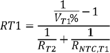
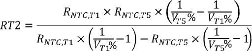
In the equations above, RNTC, T1 is the NTC thermistor resistance value at temperature T1 and RNTC, T5 is the NTC thermistor resistance value at temperature T5. Selecting a 0°C to 60°C range for a Li-ion or Li-polymer battery then:

  • RNTC,T1 = 27.28 kΩ (0°C)
  • RNTC,T5 = 3.02 kΩ (60°C)
  • RT1 = 5.3 kΩ
  • RT2 = 31.14 kΩ