SLUSCH6B March 2016 – March 2017
PRODUCTION DATA.
- 1 Features
- 2 Applications
- 3 Description
- 4 Revision History
- 5 Description (Continued)
- 6 Pin Configuration and Functions
- 7 Specifications
-
8 Detailed Description
- 8.1 Functional Block Diagram
- 8.2
Feature Description
- 8.2.1 Device Power-On-Reset (POR)
- 8.2.2 Device Power Up from Battery without Input Source
- 8.2.3 Device Power Up from Input Source
- 8.2.4 Power Path Management
- 8.2.5 Battery Charging Management
- 8.2.6 Battery Monitor
- 8.2.7 Status Outputs (PG, STAT, and INT)
- 8.2.8 Thermal Regulation and Thermal Shutdown
- 8.2.9 Voltage and Current Monitoring in Buck
- 8.2.10 Battery Protection
- 8.2.11 Serial Interface
- 8.3 Device Functional Modes
- 8.4 Register Map
- 9 Application and Implementation
- 10Power Supply Recommendations
- 11Layout
- 12Device and Documentation Support
- 13Mechanical, Packaging, and Orderable Information
Package Options
Mechanical Data (Package|Pins)
- YFF|42
Thermal pad, mechanical data (Package|Pins)
Orderable Information
9 Application and Implementation
NOTE
Information in the following applications sections is not part of the TI component specification, and TI does not warrant its accuracy or completeness. TI’s customers are responsible for determining suitability of components for their purposes. Customers should validate and test their design implementation to confirm system functionality.
9.1 Application Information
A typical application consists of the device configured as an I2C controlled power path management device and a single cell battery charger for Li-Ion and Li-polymer batteries used in a wide range of smartphones and other portable devices. It integrates an input reverse-block FET (RBFET, Q1), high-side switching FET (HSFET, Q2), low-side switching FET (LSFET, Q3), and BATFET (Q4) between the system and battery. The device also integrates a bootstrap diode for the high-side gate drive.
9.2 Typical Application Diagram
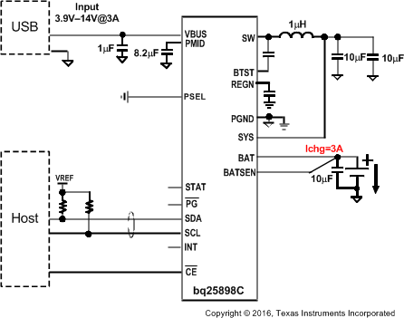 Figure 40. bq25898C Application Diagram as Slave Charger
9.2.1 Design Requirements
For this design example, use the parameters shown in Table 26.
Table 26. Design Parameters
| PARAMETER | VALUE |
|---|---|
| Input voltage range | 3.9 V to 14 V |
| Input current limit | 1.5 A |
| Fast charge current | 3000 mA |
| Output voltage | 4.208 V |
9.2.2 Detailed Design Procedure
9.2.2.1 Inductor Selection
The device has 1.5 MHz switching frequency to allow the use of small inductor and capacitor values. The Inductor saturation current should be higher than the charging current (ICHG) plus half the ripple current (IRIPPLE):

The inductor ripple current depends on input voltage (VBUS), duty cycle (D = VBAT/VVBUS), switching frequency (fs) and inductance (L):

The maximum inductor ripple current happens with D = 0.5 or close to 0.5. Usually inductor ripple is designed in the range of (20–40%) maximum charging current as a trade-off between inductor size and efficiency for a practical design.
9.2.2.2 Buck Input Capacitor
Input capacitor should have enough ripple current rating to absorb input switching ripple current. The worst case RMS ripple current is half of the charging current when duty cycle is 0.5. If the converter does not operate at 50% duty cycle, then the worst case capacitor RMS current IPMID occurs where the duty cycle is closest to 50% and can be estimated by Equation 3:

Low ESR ceramic capacitor such as X7R or X5R is preferred for input decoupling capacitor and should be placed to the drain of the high side MOSFET and source of the low side MOSFET as close as possible. Voltage rating of the capacitor must be higher than normal input voltage level. 25 V rating or higher capacitor is preferred for up to 14-V input voltage. 8.2-μF capacitance is suggested.
9.2.2.3 System Output Capacitor
Output capacitor also should have enough ripple current rating to absorb output switching ripple current. The output capacitor RMS current ICOUT is given:

The output capacitor voltage ripple can be calculated as follows:

At certain input/output voltage and switching frequency, the voltage ripple can be reduced by increasing the output filter LC. The charger device has internal loop compensator. To get good loop stability, 1-µH and minimum of 20-µF output capacitor is recommended. The preferred ceramic capacitor is 6V or higher rating, X7R or X5R.
9.2.3 Application Curves
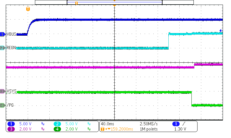
| VBAT = 3.2 V, | VBUS = 5 V |
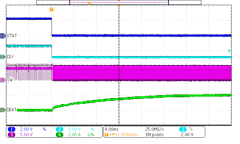
| VBUS = 5 V |
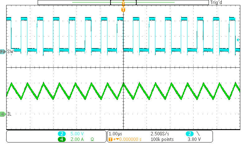
| VBUS = 12 V | VBAT = 3.8 V | ICHG = 3 A |
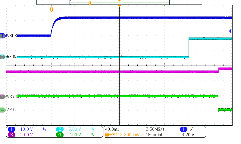
| VBAT = 3.2 V | VBUS = 12 V |
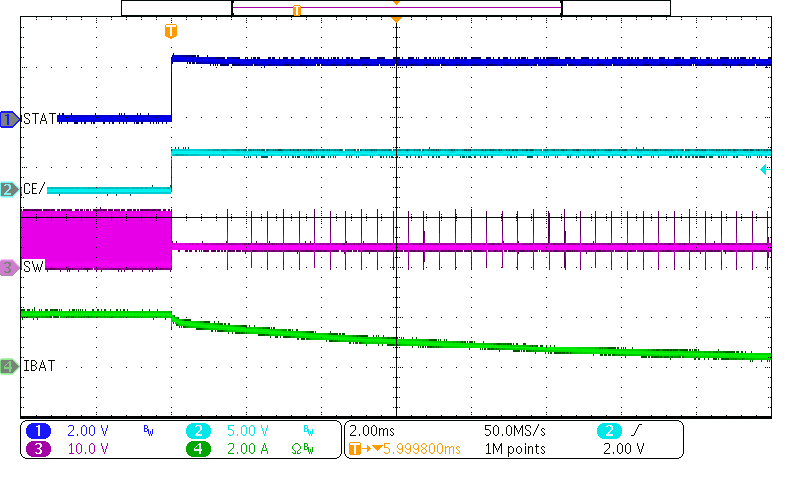
| VBUS = 12 V |
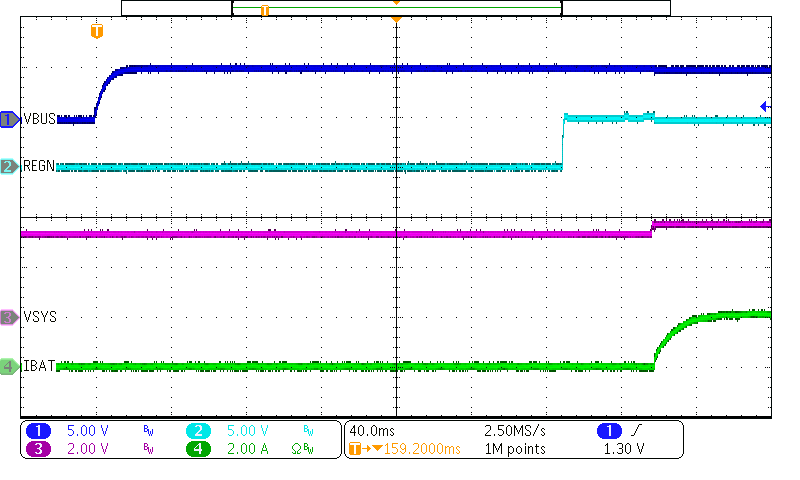
| VBAT = 3.2 V, | VBUS = 5 V |
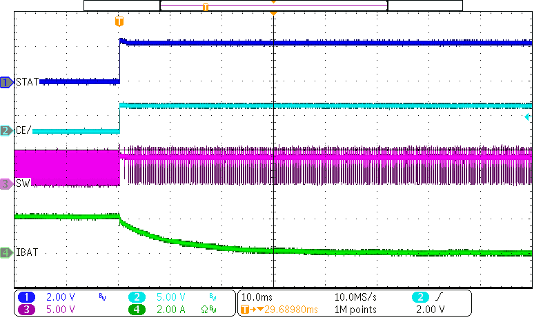
| VBUS = 5 V |
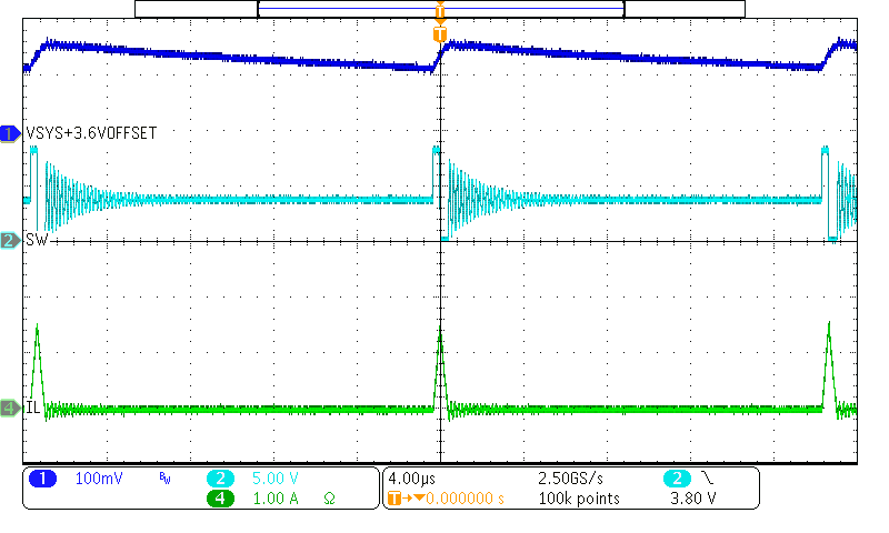
| VBUS = 9V | ISYS = 20 mA, | Charge Disable |
| No Battery |
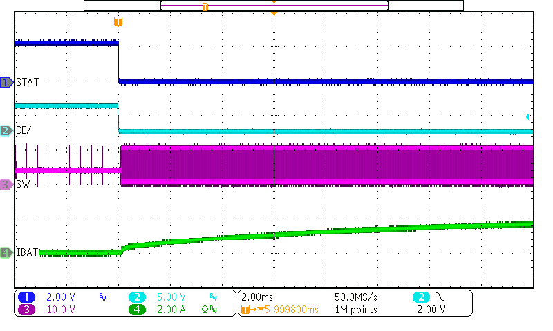
| VBUS = 12 V |
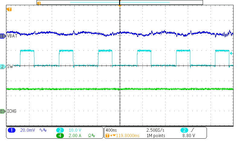
| VBUS = 12 V | VBAT = 3.8 V | ICHG = 3 A |