SLUSA96B August 2010 – April 2016 BQ32002
PRODUCTION DATA.
- 1 Features
- 2 Applications
- 3 Description
- 4 Revision History
- 5 Pin Configuration and Functions
- 6 Specifications
- 7 Detailed Description
- 8 Application and Implementation
- 9 Power Supply Recommendations
- 10Layout
- 11Device and Documentation Support
- 12Mechanical, Packaging, and Orderable Information
Package Options
Mechanical Data (Package|Pins)
- D|8
Thermal pad, mechanical data (Package|Pins)
Orderable Information
8 Application and Implementation
NOTE
Information in the following applications sections is not part of the TI component specification, and TI does not warrant its accuracy or completeness. TI’s customers are responsible for determining suitability of components for their purposes. Customers should validate and test their design implementation to confirm system functionality.
8.1 Application Information
The typical application for the BQ32002 is to provide precise time and date to a system. The backup power supply provides additional reliability by automatically switching over from the main supply when it drops under the voltage threshold.
8.2 Typical Application
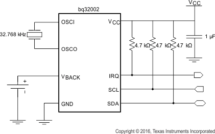
The following design is a common application of the BQ32002.
 Figure 8. Typical Application Schematic
8.2.1 Design Requirements
Table 5 lists the parameters for this design example.
Table 5. Design Parameters
| DESIGN PARAMETER | REFERENCE | EXAMPLE VALUE |
|---|---|---|
| Supply Voltage | VCC | 3.3 V |
| Backup Supply | VBACK | BR1225 |
| Crystal Oscillator | XT | 32.768 kHz |
8.2.2 Detailed Design Procedure
8.2.2.1 Reading From a Register
The report details the read-back of the SECONDS register. Figure 9 depicts the first condition that will be used as a benchmark to compare the values taken from the SECONDS register in the BQ32002, to the internal PC time of the oscilloscope. In this example two modes of operation are demonstrated.
-
Condition 1 The main power supply, VCC, is greater than the backup power supply, VBACK, and the internal reference voltage, VREF. In this mode, the device's internal registers are fully operational with READ and WRITE access. Analyzing Figure 9, the known register values are compared to the system clock; in this case, the PC clock which is shown at the bottom of the screen capture.
The BQ32002 during this condition is reading back [101][0010]= [5][2], which corresponds to 52 seconds at PC time of 2:22:43 PM.
-
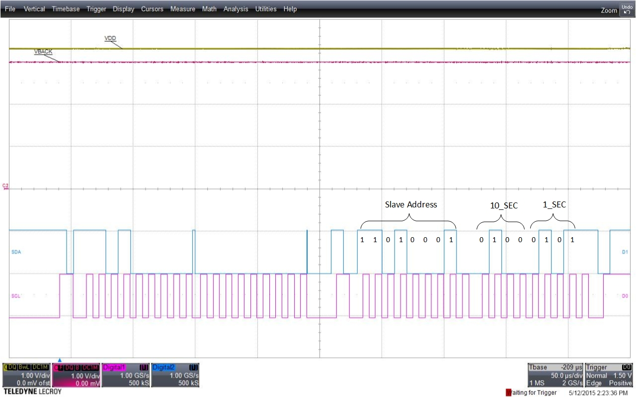
Condition 2 VCC is now lowered to 2 V (VBACK > VCC). In this mode, the I2C communications are halted. However, the internal time-keeping registers maintain full functional operation and accuracy which will be available to be reliably read by the controller 1 second after the RTC switches from VBACK to VCC supply.
-
Condition 3 During this final test condition, the RTC is restored to operate from the main power supply and I2C communications are now fully functional.
Figure 10 demonstrates a read-back value from the SECONDS register of [100][0101]= [4][5], or 45 seconds at PC time of 2:23:36 PM. This proves that the BQ32002 managed to accurately maintain the time-keeping registers functional while the VCC dropped below VBACK.
8.2.2.2 Leap Year Compensation
The BQ32002 classifies a leap year as any year that is evenly divisible by 4. Using this rule allows for reliable leap year compensation until 2100. Years that fall outside this rule will need to be compensated for by the external controller.
8.2.2.3 Utilizing the Backup Supply
In order for the BQ32002 to achieve a low backup supply current as specified in the Electrical Characteristics, the VCC pin must be initialized after every total power loss situation. Initialization Is achieved by powering on VCC with a voltage between 3 to 3.6 V for at least 1 ms immediately after the backup supply is connected. If the VCC is not powered on while connecting the backup supply, then the expected leakage current from VBACK will be much greater than specified.
8.2.3 Application Curves
 Figure 9. Master and Slave I2C Communication for the SECONDS Register
 Figure 10. Master and Slave I2C Communication for the SECONDS Register After Recovering from the Backup Supply