SLUSA96B August   2010  – April 2016 BQ32002

PRODUCTION DATA.  

  1. Features
  2. Applications
  3. Description
  4. Revision History
  5. Pin Configuration and Functions
  6. Specifications
    1. 6.1 Absolute Maximum Ratings
    2. 6.2 ESD Ratings
    3. 6.3 Recommended Operating Conditions
    4. 6.4 Thermal Information
    5. 6.5 Electrical Characteristics
    6. 6.6 Timing Requirements
    7. 6.7 Typical Characteristics
  7. Detailed Description
    1. 7.1 Overview
    2. 7.2 Functional Block Diagram
    3. 7.3 Feature Description
      1. 7.3.1 IRQ Function
      2. 7.3.2 VBACK Switchover
    4. 7.4 Device Functional Modes
    5. 7.5 Programming
      1. 7.5.1 I2C Serial Interface
    6. 7.6 Register Maps
      1. 7.6.1 I2C Read After Backup Mode
      2. 7.6.2 Normal Register Descriptions
      3. 7.6.3 Special Function Registers
  8. Application and Implementation
    1. 8.1 Application Information
    2. 8.2 Typical Application
      1. 8.2.1 Design Requirements
      2. 8.2.2 Detailed Design Procedure
        1. 8.2.2.1 Reading From a Register
        2. 8.2.2.2 Leap Year Compensation
        3. 8.2.2.3 Utilizing the Backup Supply
      3. 8.2.3 Application Curves
  9. Power Supply Recommendations
  10. 10Layout
    1. 10.1 Layout Guidelines
    2. 10.2 Layout Example
  11. 11Device and Documentation Support
    1. 11.1 Community Resources
    2. 11.2 Trademarks
    3. 11.3 Electrostatic Discharge Caution
    4. 11.4 Glossary
  12. 12Mechanical, Packaging, and Orderable Information

Package Options

Mechanical Data (Package|Pins)
Thermal pad, mechanical data (Package|Pins)
Orderable Information

10 Layout

10.1 Layout Guidelines

The VCC pin should be bypassed to GND using a low-ESR ceramic bypass capacitor with a minimum recommended value of 1 µF. This capacitor must be placed as close to the VCC and GND pins as possible with thick trace or ground plane connection to the device GND pin.

Locate the 32.768-kHz crystal oscillator as close as possible to the OSCI and OSCO pins. This will minimize stray capacitance.

10.2 Layout Example
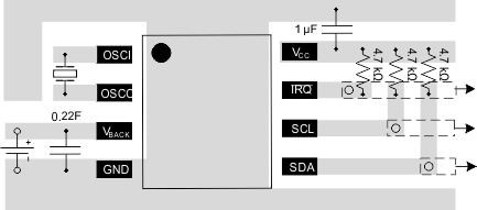
BQ32002 layout_slus900.gif Figure 11. Recommended PCB Layout