SLUSCI1B August 2016 – November 2016
PRODUCTION DATA.
- 1 Features
- 2 Applications
- 3 Description
- 4 Revision History
- 5 Pin Configuration and Functions
-
6 Specifications
- 6.1 Absolute Maximum Ratings
- 6.2 ESD Ratings
- 6.3 Recommended Operating Conditions
- 6.4 Thermal Information
- 6.5 Electrical Characteristics: Supply Current
- 6.6 Electrical Characteristics: Digital Input and Output DC Characteristics
- 6.7 Electrical Characteristics: Power-On Reset
- 6.8 Electrical Characteristics: LDO Regulator
- 6.9 Electrical Characteristics: Internal Temperature Sensor
- 6.10 Electrical Characteristics: Low-Frequency Clock Oscillator
- 6.11 Electrical Characteristics: High-Frequency Clock Oscillator
- 6.12 Electrical Characteristics: Integrating ADC (Coulomb Counter)
- 6.13 Electrical Characteristics: ADC (Temperature and Voltage Measurements)
- 6.14 Electrical Characteristics: Data Flash Memory
- 6.15 Timing Requirements: I2C-Compatible Interface Timing Characteristics
- 6.16 Typical Characteristics
- 7 Detailed Description
- 8 Application and Implementation
- 9 Power Supply Recommendations
- 10Layout
- 11Device and Documentation Support
- 12Mechanical, Packaging, and Orderable Information
Package Options
Mechanical Data (Package|Pins)
- PW|14
Thermal pad, mechanical data (Package|Pins)
Orderable Information
8 Application and Implementation
NOTE
Information in the following applications sections is not part of the TI component specification, and TI does not warrant its accuracy or completeness. TI’s customers are responsible for determining suitability of components for their purposes. Customers should validate and test their design implementation to confirm system functionality.
8.1 Application Information
The bq34110 gas gauge is a highly configurable device with multiple features that can be used individually or simultaneously (with some restrictions). The CEDV gas gauging function together with its support for an external voltage divider allows gauging of high voltage, multi-cell battery configurations of various chemistries. The EOS Determination function is intended for rarely discharged applications and evaluates the condition of the battery without requiring conventional maintenance cycles. These and additional features are described in detail in the bq34110 Technical Reference Manual (SLUUBF7).
8.2 Typical Applications
Figure 11 is a simplified schematic of the bq34110 system used in a multi-cell configuration.
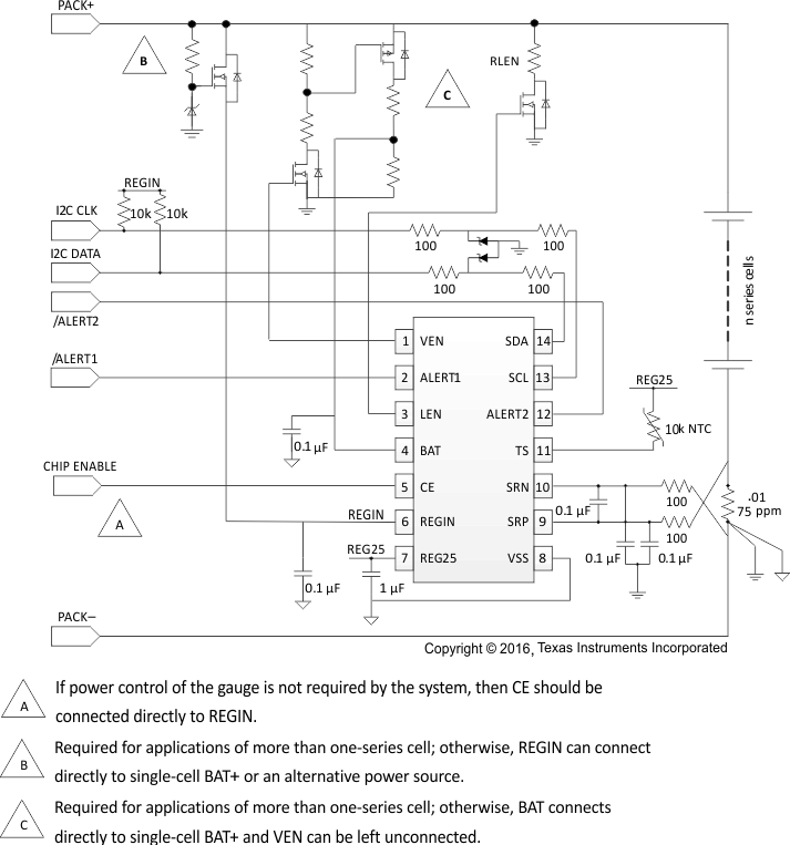 Figure 11. bq34110 Simplified System Diagram
Figure 12 shows the schematic of the bq34110 EVM, and depicts how the device can be used in the system.
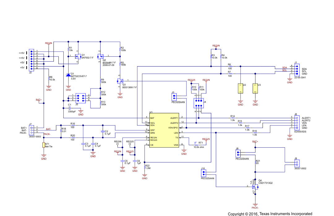 Figure 12. bq34110 EVM Schematic
8.2.1 Design Requirements
The bq34110 device supports several circuit configuration options that can be decided upon during the system design phase. Using the device with a single-cell battery versus a multi-cell configuration determines if there is a need for a battery divider and associated control using the VEN pin (as shown in Figure 11). The functions used within the bq34110 device also determine the pin usage, with the device incorporating flexibility to reuse pins for other purposes if the system configuration permits. For example, if a single-cell configuration is selected, then the VEN pin can be used as part of a direct charge control scheme. Similarly, the LEN, ALERT1, and/or ALERT2 pins can also be repurposed to support direct charge control. For additional design guidelines, refer to the bq34110 EVM User’s Guide (SLUUBI1).
8.2.2 Detailed Design Procedure
8.2.2.1 BAT Voltage Sense Input
A ceramic capacitor at the input to the BAT pin is used to bypass AC voltage ripple to ground, greatly reducing its influence on battery voltage measurements. It proves most effective in applications with load profiles that exhibit high-frequency current pulses (that is, cell phones) but is recommended for use in all applications to reduce noise on this sensitive high-impedance measurement node. If the device is used in a multi-cell configuration with an external resistive voltage divider, it is recommended that the resistors used therein be selected with temperature coefficient of resistance (TCR) of 75-ppm or below. More detail on the design of the voltage divider network is discussed in the bq34110 Technical Reference Manual (SLUUBF7).
8.2.2.2 SRP and SRN Current Sense Inputs
The filter network at the input to the coulomb counter is intended to improve differential mode rejection of voltage measured across the sense resistor. These components should be placed as close as possible to the coulomb counter inputs, and the routing of the differential traces length-matched to best minimize impedance mismatch-induced measurement errors.
8.2.2.3 Sense Resistor Selection
Any variation encountered in the resistance present between the SRP and SRN pins of the fuel gauge will affect the resulting differential voltage, and derived current, it senses. As such, it is recommended to select a sense resistor with minimal tolerance and temperature coefficient of resistance (TCR) characteristics. The standard recommendation based on the best compromise between performance and price is a 1% tolerance, 75-ppm drift sense resistor with a 1-W power rating.
8.2.2.4 TS Temperature Sense Input
Similar to the BAT pin, a ceramic decoupling capacitor for the TS pin is used to bypass AC voltage ripple away from the high-impedance ADC input, minimizing measurement error. It should be placed as close as possible to the respective input pin for optimal filtering performance.
8.2.2.5 Thermistor Selection
The fuel gauge temperature sensing circuitry is designed to work with a negative temperature coefficient-type (NTC) thermistor with a characteristic 10-kΩ resistance at room temperature (25°C). The default curve-fitting coefficients configured in the fuel gauge specifically assume a 103AT-2 type thermistor profile and so that is the default recommendation for thermistor selection purposes. Moving to a separate thermistor resistance profile (for example, JT-2 or others) requires an update to the default thermistor coefficients in data flash to ensure highest accuracy temperature measurement performance.
8.2.2.6 REGIN Power Supply Input Filtering
A ceramic capacitor is placed at the input to the fuel gauge internal LDO to increase power supply rejection (PSR) and improve effective line regulation. It ensures that voltage ripple is rejected to ground instead of coupling into the internal supply rails of the fuel gauge.
8.2.2.7 REG25 LDO Output Filtering
A ceramic capacitor is also needed at the output of the internal LDO to provide a current reservoir for fuel gauge load peaks during high peripheral utilization. It acts to stabilize the regulator output and reduce core voltage ripple inside the fuel gauge.
8.2.3 Application Curves
