SLUSCI1B August 2016 – November 2016
PRODUCTION DATA.
- 1 Features
- 2 Applications
- 3 Description
- 4 Revision History
- 5 Pin Configuration and Functions
-
6 Specifications
- 6.1 Absolute Maximum Ratings
- 6.2 ESD Ratings
- 6.3 Recommended Operating Conditions
- 6.4 Thermal Information
- 6.5 Electrical Characteristics: Supply Current
- 6.6 Electrical Characteristics: Digital Input and Output DC Characteristics
- 6.7 Electrical Characteristics: Power-On Reset
- 6.8 Electrical Characteristics: LDO Regulator
- 6.9 Electrical Characteristics: Internal Temperature Sensor
- 6.10 Electrical Characteristics: Low-Frequency Clock Oscillator
- 6.11 Electrical Characteristics: High-Frequency Clock Oscillator
- 6.12 Electrical Characteristics: Integrating ADC (Coulomb Counter)
- 6.13 Electrical Characteristics: ADC (Temperature and Voltage Measurements)
- 6.14 Electrical Characteristics: Data Flash Memory
- 6.15 Timing Requirements: I2C-Compatible Interface Timing Characteristics
- 6.16 Typical Characteristics
- 7 Detailed Description
- 8 Application and Implementation
- 9 Power Supply Recommendations
- 10Layout
- 11Device and Documentation Support
- 12Mechanical, Packaging, and Orderable Information
Package Options
Mechanical Data (Package|Pins)
- PW|14
Thermal pad, mechanical data (Package|Pins)
Orderable Information
10 Layout
10.1 Layout Guidelines
Attention to layout is critical to the success of any battery management circuit board. The mixture of high-current paths with an ultralow-current microcontroller creates the potential for design issues that are not always trivial to solve. Some of the key areas of concern are described in the following sections and can help to enable success.
10.1.1 Power Supply Decoupling Capacitor
Power supply decoupling from REG25 to ground is important for optimal operation of the gas gauge. To keep the loop area small, place this capacitor next to the IC and use the shortest possible traces. A large loop area renders the capacitor useless and forms a small-loop antenna for noise pickup. Ideally, the traces on each side of the capacitor should be the same length and run in the same direction to avoid differential noise during ESD. If possible, place a via near the VSS pin to a ground plane layer.
10.1.2 Capacitors
Power supply decoupling for the gas gauge requires 0.1-μF ceramic capacitors for the BAT and REGIN pins. These should be placed reasonably close to the IC without using long traces back to VSS. The LDO voltage regulator, whether external or internal to the main IC, requires a 1-μF ceramic capacitor to be placed fairly close to the regulation output pin (REG25). This capacitor is for amplifier loop stabilization and as an energy well for the 2.5-V supply.
10.1.3 Communication Line Protection Components
5.6-V Zener diodes are included on the I2C lines to protect the communication pins of the gas gauge from ESD. These diodes should be located as close as possible to the pack connector. The grounded end of these Zener diodes should be returned to the PACK(–) node rather than to the low-current digital ground system. This way, ESD is diverted away from the sensitive electronics as much as possible.
10.2 Layout Example
10.2.1 Ground System
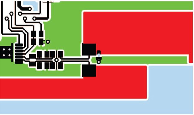
The gas gauge requires a low-current ground system separate from the high-current PACK(–) path. ESD ground is defined along the high-current path from the PACK(–) terminal to the sense resistor. It is important that the low-current ground systems only connect to the PACK(–) path at the sense resistor Kelvin pick-off point. It is recommended to use an optional inner layer ground plane for the low-current ground system.
In Figure 19, the green area shows an example of using the low-current ground as a shield for the gas gauge circuit. Notice how it is kept separate from the high-current ground, which is shown in red. The high current path is joined with the low-current path only at one point, shown with the small blue connection between the two planes.
 Figure 19. High-Current Versus Low-Current Ground Layout
10.2.2 Kelvin Connections
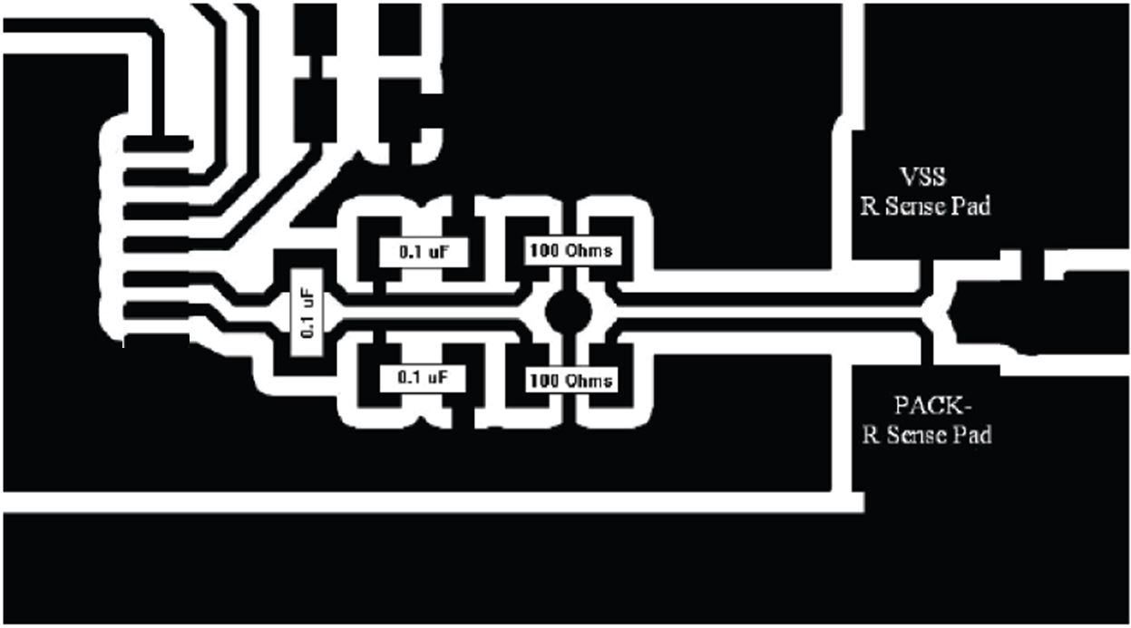
Kelvin voltage sensing is very important to accurately measure current and cell voltage. Note that in Figure 19 the differential connections at the sense resistor do not add any voltage drop across the copper etch that carries the high current path through the sense resistor.
10.2.3 Board Offset Considerations
Although the most important component for board offset reduction is the decoupling capacitor for REGIN, additional benefit is possible by using this recommended pattern for the coulomb counter differential low-pass filter network.
Maintain the symmetrical placement pattern shown for optimum current offset performance. Use symmetrical shielded differential traces, if possible, from the sense resistor to the 100-Ω resistors, as shown in Figure 20.
 Figure 20. Differential Connection Between SRP and SRN Pins with Sense Resistor
10.2.4 ESD Spark Gap
Protect the communication lines from ESD with a spark gap at the connector. Figure 21 shows the recommended pattern with its 0.2-mm spacing between the points.
 Figure 21. Recommended Spark-Gap Pattern Helps Protect Communication Lines from ESD